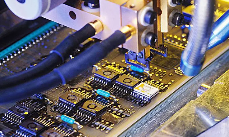
The growing demand for miniaturization in PCBs has led to the development of increasingly intricate PCB layouts. These complex designs often involve the integration of holes within BGA (Ball Grid Array) pads. Vias, an essential element of a PCB, play a vital role in connecting pads, polygons, and traces across different layers of the board.
Vias serve as connections between multiple layers in a PCB, especially in the case of multilayer boards that typically consist of at least two copper layers. By utilizing vias, PCBs can be fabricated with more than one layer of copper, allowing for enhanced functionality and versatility.
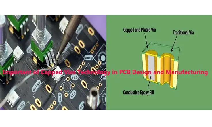
Among the different types of vias available, the focus of this article is on capped vias. Capped vias are particularly valuable in facilitating the implementation of via in pad designs due to their flat surface. These vias provide a smooth and reliable surface for creating connections, especially when it is necessary to incorporate vias directly within the pad areas of the PCB layout.
What is Capped Via (Via in Pad) ?
Capped vias technology has emerged as a valuable solution for designing via in pad (VIP) layouts due to its flat surface properties. There are two primary technological approaches utilized today: copper via filling and resin via filling with copper capping.
The demand for miniaturized printed circuit boards, especially in specific industry sectors, has spurred the creation of highly intricate PCB layouts. These layouts often incorporate interconnecting holes within BGA pads. This approach enables the same pad to serve multiple purposes: facilitating the internal circuitry of the board by establishing connections between different layers and accommodating surface mount technology (SMT) component placement. The primary advantage of this approach is a substantial reduction in board size. However, it comes with the trade-off of increased complexity in the SMD component mounting process and the potential introduction of reliability issues in the assembled board.
In scenarios where a hole exists within a pad where an SMD component needs to be mounted, a notable volume of epoxy adhesive can flow into the hole. This can lead to the formation of voids, commonly referred to as dry joints. These voids can adversely affect the component’s reliability and may result in sudden disconnection of the component from the board.
Therefore, employing capped vias, with their flat surface structure, is crucial to address these concerns. By utilizing copper via filling or resin via filling with copper capping techniques, the risk of epoxy glue flowing into the hole and generating voids is significantly minimized. This ensures a more reliable connection between the SMD component and the PCB, minimizing the potential for reliability issues during operation.
Capped Via Types
There are different types of capped vias that are used in electronic devices, and the choice of which type to use depends on various factors such as cost, size, and application. Here are some common types of capped vias:
Filled and Capped Vias: These types of capped vias are filled with a conductive material, such as copper, and then capped with a protective layer. The conductive material helps to ensure that the electrical signals can pass through the via, while the protective layer helps to prevent any contaminants from entering and causing damage to the device.
Non-conductive Capped Vias: These types of capped vias are capped with a non-conductive material, such as a polymer or ceramic. They are typically used in applications where electrical isolation is required between different layers of the device.
Stacked Vias: Stacked vias are a type of capped via that is used to connect multiple layers of the device’s circuitry. They consist of multiple vias that are stacked on top of each other and then capped with a protective layer.
Blind and Buried Vias: Blind and buried vias are types of capped vias that are used in multi-layer PCBs. Blind vias connect the outer layer of the PCB to an inner layer, while buried vias connect two inner layers of the PCB. Both types of vias are capped with a protective layer to prevent any contaminants from entering and causing damage to the device.
All in all, there are different types of capped vias that are used in electronic devices, depending on the specific application and requirements of the device. Some common types include filled and capped vias, non-conductive capped vias, stacked vias, and blind and buried vias.
Capped Via Vs. Non-Capped Via: Which is the Better Choice ?
The optimal choice between capped and non-capped vias for your specific PCB design depends on various factors. Each type of via offers its own set of benefits and considerations. Here is a comprehensive comparison:
Comparison of Capped and Non-capped Vias for PCB Designs
The choice between capped and non-capped vias in your PCB design depends on several factors. Each type of via offers distinct advantages and considerations. Here is a comprehensive analysis:
Capped vias are particularly suitable for high-frequency PCB designs due to their ability to mitigate signal loss and improve overall performance.
Non-capped vias may be more appropriate for low-frequency PCB designs, as the benefits of using capped vias may not justify the additional cost incurred.
Trade-offs Between Cost and Performance
Capped vias generally involve higher costs compared to non-capped vias because of additional manufacturing steps and materials required.
However, the enhanced performance and reliability provided by capped vias may justify the investment in specific applications.
Impact of Capped Vias on PCB Reliability and Durability
Capped vias contribute to reducing the risk of copper oxidation and micro-crack formation, thereby enhancing the overall reliability and durability of the PCB.
Non-capped vias may be more prone to oxidation and cracking, which can potentially lead to premature failure of the PCB.
Future Developments in Capped Via Technology
Continual advancements in capped via technology, such as material improvements and manufacturing processes, are expected to reduce costs and further enhance the performance of capped vias.
As PCB designs become more complex and the demand for higher performance grows, capped vias are anticipated to gain popularity among designers.
Ultimately, as a PCB engineer, the decision regarding the use of capped or non-capped vias lies in your hands. Taking into account the specific requirements and constraints of your design, you are best positioned to make the final determination.
How the Capped Via work ?
Capped vias are a commonly utilized type of via in printed circuit boards (PCBs). They involve the application of epoxy or a similar material over the top of the via to provide protection against detrimental factors such as moisture, dust, and debris.
The necessity of capped vias arises from the inherent vulnerabilities of regular vias, which are essentially drilled holes in the PCB. These openings are susceptible to becoming filled with unwanted substances or being damaged over time through wear and tear. Such issues can detrimentally impact the performance of the PCB, especially in challenging environments. Capped vias address these concerns by offering a protective shield.
Another notable benefit of using capped vias is their potential to mitigate electromagnetic interference (EMI) generated by the PCB. EMI can cause significant problems in electronic devices, affecting various aspects such as radio transmissions and the performance of sensitive components. By implementing capped vias, it becomes possible to reduce EMI, thus enhancing the overall functionality of the PCB.
It is important to acknowledge that capped vias are not always essential and, in certain cases, may be considered excessive. However, they prove particularly valuable when designing PCBs for rugged environments or when EMI reduction is a critical consideration. In such scenarios, opting for capped vias can be a prudent decision.
Design and Fabrication Process for Capped Vias Technology
Capped vias technology is a type of via technology used in the manufacturing of electronic devices, such as printed circuit boards (PCBs). It involves the use of an additional protective layer on top of a via, which helps to prevent contaminants from entering and causing damage to the device.
The design and fabrication process for capped vias technology involves several steps. Here’s an overview of each step:
PCB Design: The first step in the process is designing the PCB. This involves creating a layout of the device’s circuitry using specialized software. The layout includes the location and size of each via.
Drilling: Once the PCB design is complete, the next step is drilling the vias. This is done using a laser or mechanical drill, which creates a hole through the layers of the PCB. The size of the via depends on the requirements of the device.
Plating: After the vias are drilled, they are plated with a conductive material, such as copper. This helps to ensure that the electrical signals can pass through the via.
Applying the Cap: Once the vias are plated, the next step is to apply the cap. This is done by depositing a thin layer of a protective material, such as a polymer or metal, on top of the via. The cap helps to prevent any contaminants from entering the via and causing damage to the device.
Curing: After the cap is applied, it is cured or hardened. This is done using heat or ultraviolet light, depending on the type of material used for the cap. Once the cap is cured, it becomes a permanent layer on top of the via.
Final Steps: Once the capped vias are fabricated, the device undergoes several final steps, such as soldering components onto the PCB and testing the device’s functionality.
To sum up, the design and fabrication process for capped vias technology involves drilling vias, plating them with conductive material, applying a protective cap, and curing the cap to create a permanent layer on top of the via. This process helps to improve the reliability and performance of electronic devices.
Benefts of Using Capped Vias in PCB Design and Manufacturing
In PCB design and manufacturing, the utilization of capped vias provides numerous advantages. Here are some key benefits that can be achieved:
Enhanced Reliability: Capped vias contribute to improved reliability by safeguarding electronic devices against environmental contaminants such as dust, moisture, and chemicals. This protective measure helps prevent damage to the devices and reduces the risk of failure over time.
Improved Performance: Capped vias have the potential to enhance the performance of electronic devices by enabling faster signal transmission between different components. This results in faster processing times and overall improved performance of the devices.
Size Reduction: Capped vias assist in reducing the size of PCBs, which is crucial in applications where space is limited. By implementing capped vias, designers can create smaller and more compact PCBs without compromising reliability or performance.
Cost Savings: Although the initial cost of using capped vias may be higher compared to traditional vias, the long-term cost savings can be substantial. Capped vias help decrease the risk of device failures and the need for repairs, leading to significant time and cost savings for manufacturers in the long run.
Enhanced Design Flexibility: Capped vias offer greater design flexibility than traditional vias, as they can be employed across a broad range of applications and can be customized to meet specific design requirements. This enables designers to create more intricate and advanced electronic devices.
To summarize, incorporating capped vias in PCB design and manufacturing provides several benefits, including enhanced reliability, improved performance, size reduction, cost savings, and increased design flexibility. These advantages make capped vias an appealing choice for electronic device manufacturers seeking to optimize their products.
How Many Method Testing and Inspection of Capped Vias ?
Testing and inspection of capped vias are crucial steps in the manufacturing process of electronic devices. These procedures help ensure the quality and reliability of the PCBs. Various non-destructive and destructive testing methods are employed for comprehensive evaluation.
Non-destructive testing methods
X-ray inspection: This method allows for non-destructive inspection of the via’s interior, detecting voids or defects without damaging the PCB.
Automated optical inspection (AOI): Cameras are utilized to visually inspect the PCB for defects, including those within the vias.
Destructive testing methods
Cross-sectional analysis: This method involves cutting the PCB and via to examine them under a microscope, providing insights into via plating quality and identifying any defects.
Microsectioning: Similar to cross-sectional analysis, this technique employs a focused ion beam (FIB) to create a thin slice of the via for examination.
Additional inspection techniques
Electrical testing: Conducting tests to ensure proper continuity and resistance of the vias, verifying their functional integrity.
Thermal testing: Measuring the temperature of the via during operation to ensure it remains within safe limits and does not overheat.
Pull testing: Applying force to the via to ensure secure attachment to the PCB.
Quality control standards
For those utilizing the services of a Contract Manufacturer (CM) or professional manufacturer, adherence to quality control standards is essential:
IPC-6012: Standard for rigid printed boards, specifies requirements for capped vias, such as plating thickness and hole size tolerance.
IPC-A-600: Standard for visually inspecting electronic assemblies, including PCBs.
IPC-A-610: Standard for acceptability of electronic assemblies.
IPC-6013: Qualification and Performance Specification for Flexible Printed Boards, which may utilize capped vias.
IPC-6018: Standard for High-Frequency (Microwave) Printed Boards, often employed in military applications, as mentioned previously.
Common Applications of Capped Vias in PCBs
Capped vias are commonly used in the manufacturing of printed circuit boards (PCBs) in a wide range of electronic devices. Here are some real-world applications of capped vias in PCBs:
Smartphones: Smartphones are one of the most common applications of capped vias in PCBs. Capped vias are used to connect different layers of the smartphone’s circuitry, which allows for faster signal transmission and improved performance. They also help to protect the device from environmental contaminants, such as dust and moisture.
Computers: Computers and other computing devices use PCBs to connect different components. Capped vias are used in these PCBs to provide reliable connections between the different layers of the board. They also help to reduce the size of the PCBs, which is important in applications where space is limited.
Medical Devices: Many medical devices, such as implantable devices and diagnostic equipment, use PCBs to connect different components. Capped vias are used in these PCBs to ensure reliable connections and protect the devices from environmental contaminants.
Automotive Electronics: Automotive electronics, such as engine control units and infotainment systems, use PCBs to connect different components. Capped vias are used in these PCBs to provide reliable connections and protect the devices from environmental contaminants, such as moisture and dust.
Aerospace and Defense: Aerospace and defense applications, such as avionics and communication systems, use PCBs to connect different components. Capped vias are used in these PCBs to provide reliable connections and protect the devices from environmental contaminants, such as radiation and extreme temperatures.
So Why is Capped Via Technology Crucial in PCB Fabrication ?
Capped via technology is crucial in PCB fabrication for several reasons:
Enhanced Reliability: Capped vias help improve the reliability of PCBs by preventing the ingress of contaminants, such as solder mask, flux residue, or moisture, into the vias and subsequent damage to the internal circuitry. The caps act as protective barriers, reducing the risk of short circuits or electrical failures.
Improved Signal Integrity: In high-speed or high-frequency PCB designs, signal integrity is paramount. Capped vias minimize signal loss and electromagnetic interference (EMI) by effectively isolating adjacent signal layers, reducing crosstalk, and maintaining controlled impedance.
Plating Thickness Control: The use of capped vias allows for better control over the plating thickness within the via. This is particularly important in complex PCB layouts where multiple layers and fine-pitch components are involved. Consistent plating thickness ensures reliable electrical connections and helps avoid issues like excessive solder voids or weak solder joints.
Solder Joint Integrity: Capped vias provide a stable platform for solder joints. By preventing the epoxy glue or other contaminants from seeping into the vias, the risk of voids, dry joints, or sudden breaks in component connections is significantly reduced. This improves the overall robustness and longevity of the PCB assembly.
Miniaturization and High-Density Designs: As the demand for miniaturization increases, PCBs are becoming more densely packed with smaller components. Capped vias offer a solution to maintain effective interconnectivity within limited space while minimizing the potential for short circuits or soldering issues.
Capped Vias: A solution to complex PCB manufacturing
In certain cases, the use of capped vias technology becomes essential for achieving planarity in the surface-mounted device (SMD) components that require it. This technology plays a significant role in the manufacturing of complex printed circuit boards (PCBs). It involves filling the via hole with an appropriate amount of resin and subsequently plating it. A thin copper cap is then deposited on the pad. One of the key advantages of capped vias technology is its ability to preserve the interconnections created by the via hole. Additionally, it ensures a perfectly flat pad surface, facilitating the easy mounting of each component.
The integration of capped vias technology is also beneficial in cases such as buried vias, rather than laser vias (BGA pads). When the SBU (Sequential Build-Up) technology is applied, micro-breaks can occur at the corners of buried vias, potentially affecting their plating. This poses a risk of PCB assembly (PCBA) unreliability and malfunctioning interconnections. To mitigate this issue, resin is utilized to fill the buried vias, ensuring their robustness and preserving the desired performance of the board.
By employing capped vias technology, these potential problems can be effectively addressed, resulting in reliable PCBA and the maintenance of optimal interconnectivity throughout the board.
Overall, capped via technology plays a crucial role in PCB fabrication by ensuring improved reliability, signal integrity, plating control, solder joint quality, and compatibility with miniaturized and high-density designs.
Final Thoughts
Capped vias have become an essential component of modern PCB design, and their applications continue to expand across various industries. When seeking to ensure optimal performance of electronic systems, it is crucial to collaborate with a reputable PCB manufacturer capable of delivering high-quality capped via PCBs.
When selecting a suitable PCB manufacturer for your capped via PCB requirements, several factors should be considered. These include the manufacturer’s industry experience, reputation, and the quality of their facilities and equipment. At JarnisTech, we have an extensive track record of providing exceptional PCB manufacturing services, serving customers since 2003 from our cutting-edge facilities located in Shenzhen.
Our state-of-the-art facilities are equipped with advanced technology, and our team consists of experienced professionals who are dedicated to maintaining the highest standards of quality. We take pride in delivering superior results for our clients, making us a reliable choice for your next PCB project.
Regardless of the industry you operate in, whether it is medical, aerospace, automotive, or industrial, we possess the expertise and resources to meet your specific requirements. Contact us today, and we will be more than capable of assisting you with any PCB needs you may have.