
Ceramic PCBs have become a standout choice for high-performance electronics, particularly in fields where precision, resilience, and advanced functionality are non-negotiable. Industries such as aerospace, automotive, power electronics, and LED lighting rely on these advanced circuit boards to meet demanding performance standards. This article unpacks the core design principles, explores the materials and cutting-edge manufacturing techniques, and highlights the diverse types of ceramic PCBs.
Whether you’re curious about the science behind their durability or intrigued by their role in emerging technologies, this deep dive promises to shed light on why ceramic PCBs are shaping the future of electronics. Buckle up as we explore this dynamic and innovative technology!
Why Ceramic PCBs Are Revolutionizing Modern Electronics?
In the world of electronics, demands for higher efficiency, compact designs, and enhanced thermal management are more pressing than ever. Ceramic PCBs stand as a transformative solution, bridging the gap where traditional PCBs like FR4 and metal-core boards fall short. Known for their high thermal conductivity, mechanical durability, and electrical insulation, ceramic PCBs are the backbone of high-performance systems in industries like aerospace, automotive, and power electronics. The following sections explore how these advanced substrates go beyond conventional options, the key benefits they offer, and their application in cutting-edge industries.
Beyond Conventional Circuit Boards
Ceramic PCBs take the stage when traditional options like FR4 and metal-core PCBs hit their limits. While FR4 substrates are commonly used for their cost-effectiveness and ease of fabrication, they struggle with heat management and structural stability, especially in extreme environments. Metal-core boards, while better at dissipating heat, can lack the precision and dimensional stability needed for applications demanding exceptional accuracy and reliable electrical insulation.
Ceramic PCBs rise to the occasion in challenging environments. For example, in aerospace systems, where electronic circuits must operate flawlessly in the vacuum of space, ceramic substrates deliver the reliability required to endure wide temperature variations and high-frequency performance without breaking a sweat. Similarly, in electric vehicles (EVs), ceramic PCBs are a go-to solution for battery management systems, where efficient heat dissipation prevents overheating and ensures longevity.
| Comparison of PCB Substrate Properties | FR4 | Metal-Core PCBs | Ceramic PCBs |
| Thermal Conductivity | Low (~0.3 W/mK) | Medium (~2-5 W/mK) | High (up to 230 W/mK) |
| Dielectric Strength | Moderate | Moderate | Excellent |
| Thermal Stability | Limited | Moderate | Outstanding |
| Application Suitability | General-purpose | Moderate-power devices | High-power, high-reliability applications |
With these attributes, ceramic PCBs outlast and outperform their competitors in tough environments, making them the obvious choice for industries that refuse to compromise.
Top Advantages You Can Bank On
Ceramic PCBs offer a buffet of benefits that make them a preferred choice for designers and engineers alike.
1.Unmatched Thermal Performance-
When you’re dealing with high-powered devices, heat is the enemy. Ceramic substrates like aluminum nitride (AlN) and alumina (Al₂O₃) excel in transferring heat away from electronic components. This characteristic not only boosts performance but also increases the lifespan of sensitive electronics.
2.Durability and Resilience-
Built to last, ceramic PCBs can endure thermal cycling and mechanical stress better than traditional materials. Whether it’s the extreme vibrations of a rocket launch or the wear and tear of industrial machinery, these boards handle it all.
3.Superior Electrical Insulation-
Ceramic substrates offer high dielectric strength, reducing the risk of short circuits and ensuring stable operation even under high voltage. This is particularly advantageous in LED lighting systems and medical devices, where reliability is non-negotiable.
4.Compact and Lightweight Design-
Ceramic PCBs offer excellent thermal conductivity, which reduces the need for extra cooling systems, leading to more compact and efficient designs. This is especially valuable in aerospace applications, where every gram and centimeter counts. By efficiently managing heat, ceramic PCBs help minimize the size and weight of the systems while maintaining top-level performance in demanding environments.
So, whether you’re building an LED array for a next-gen surgical tool or designing power modules for renewable energy, ceramic PCBs are your ace in the hole.
A Perfect Fit for Cutting-Edge Industries
Ceramic PCBs aren’t just another option—they’re the backbone of some of the most innovative industries out there.
●Aerospace Adventures-
When it comes to satellite systems, radar modules, and avionics, ceramic PCBs excel in environments where performance and reliability are non-negotiable. Take satellite communication systems, for example. Ceramic substrates keep the signals strong and clear while standing up to radiation exposure, which can be a real challenge in space. Even when millions of miles away from Earth, these systems continue to function seamlessly, thanks to the robust nature of ceramic PCBs. They offer peace of mind, ensuring that high-stakes missions stay on track, no matter the conditions.
●Automotive Breakthroughs-
In electric and autonomous vehicles, ceramic PCBs are fundamental in managing power systems effectively. Applications include power inverters, ADAS modules, and battery management systems. The thermal and electrical properties of ceramic substrates ensure that these critical systems perform without a hitch, even under heavy loads.
●Lighting the Way in LEDs-
LED lighting systems, especially high-power applications, benefit significantly from ceramic PCBs. Their superior heat management enables brighter, longer-lasting lights, which are increasingly used in automotive headlights, stadium floodlights, and even surgical lighting.
Materials That Define Ceramic PCBs
The foundation of every ceramic PCB lies in its substrate material, which directly impacts its performance, durability, and application scope. Whether you’re designing for high-temperature environments, high-frequency systems, or heavy-duty industrial settings, the material you choose can make all the difference. Let’s break down the most popular options and their unique features, so you’ll know what’s best for your next project.
Alumina (Al₂O₃): The Reliable Workhorse
Alumina is the seasoned veteran of ceramic PCB materials. Known for its balance of affordability and functionality, this material delivers consistent thermal performance and mechanical stability, making it a favorite for industries with tight budgets yet demanding requirements.
One of the standout features of alumina is its thermal conductivity, which ranges between 20-30 W/mK. While not as high as aluminum nitride, it’s more than enough for applications like LED modules, automotive lighting, and consumer electronics. Additionally, its robust dielectric strength ensures reliable insulation in power circuits.
For instance, automotive manufacturers often rely on alumina-based PCBs for LED headlights due to their ability to handle high temperatures without cracking or warping. The affordability of alumina also allows engineers to scale production without ballooning costs. Here’s a quick look at why alumina shines:
| Property | Value | Applications |
| Thermal Conductivity | 20-30 W/mK | LED modules, automotive lighting |
| Dielectric Strength | ~15 kV/mm | Power circuits |
| Cost | Low | Consumer electronics |
So, if you’re after a material that gets the job done without breaking the bank, alumina is the go-to choice.
Aluminum Nitride (AlN): The Heat Conductor’s Dream
When it comes to heat dissipation, aluminum nitride (AlN) truly stands out. With thermal conductivity reaching up to 230 W/mK, AlN outperforms other substrates by a wide margin. It’s no wonder this material is a favorite in power electronics and aerospace systems.
Imagine a power inverter in an electric vehicle running at full capacity during a hot summer day. The heat generated by the device would fry ordinary PCBs, but AlN-based boards wick away heat faster than you can say “overheat.” This keeps components cooler and extends the system’s lifespan.
Aluminum nitride isn’t just about heat management—it’s also lightweight and mechanically strong. This makes it an excellent fit for satellite components, where reducing weight while ensuring durability is a top priority. Below is a comparison of AlN’s properties:
| Property | Value | Applications |
| Thermal Conductivity | Up to 230 W/mK | Power inverters, aerospace modules |
| Dielectric Strength | ~18 kV/mm | High-frequency circuits |
| Cost | Higher than alumina | High-power systems |
If your project demands top-tier heat dissipation and reliability, aluminum nitride has got you covered.
The Rookies: Beryllium Oxide and Silicon Carbide
While alumina and aluminum nitride dominate the market, emerging materials like beryllium oxide (BeO) and silicon carbide (SiC) are proving their mettle in niche applications. These materials may come with higher costs, but their unique properties make them indispensable for certain cutting-edge industries.
●Beryllium Oxide (BeO): BeO offers an astonishing thermal conductivity of up to 330 W/mK, making it the king of heat dissipation. It’s often used in high-power RF amplifiers and microwave devices, where excessive heat can compromise performance. However, due to its toxicity during manufacturing, BeO’s usage is limited to specialized applications.
●Silicon Carbide (SiC): Silicon carbide (SiC) stands out for its incredible mechanical strength and ability to handle extreme temperatures. This material proves itself in demanding environments, such as in industrial power modules and high-temperature sensors. For example, in a jet engine monitoring system, SiC-based PCBs keep performing reliably even when temperatures soar above 2000°F. Whether it’s withstanding heat in high-powered machinery or staying strong under pressure, SiC brings the toughness needed to keep things intact when the heat is on. In these intense settings, SiC simply doesn’t back down, offering unmatched durability and stability where it’s needed most.
Here’s how these rookies stack up:
| Material | Thermal Conductivity | Key Strengths | Applications |
| Beryllium Oxide (BeO) | ~330 W/mK | Exceptional heat dissipation | RF amplifiers, microwave devices |
| Silicon Carbide (SiC) | ~120 W/mK | High mechanical and thermal resilience | Industrial power systems, jet sensors |
While these materials aren’t for every project, they bring unparalleled advantages to specialized industries. For we pushing the boundaries of performance, we’re worth every penny.
Designing Ceramic PCBs for High-Performance Systems
In the world of high-performance electronics, the design of your PCB isn’t just about getting the right material—it’s about carefully optimizing every aspect to handle demanding applications. Ceramic PCBs are known for their ability to excel in heat management, signal integrity, and compactness. Let’s break down how you can leverage ceramic PCBs in your designs to make them stand out in industries like automotive, aerospace, and telecommunications.
Managing Heat Like a Pro
When it comes to designing PCBs for high-power systems, heat management isn’t just a feature—it’s a requirement. If your board can’t handle the heat, you’re looking at potential failures, performance degradation, and costly repairs. Ceramic PCBs are built to tackle this challenge head-on, thanks to their remarkable heat transfer properties.
The standout feature of ceramic PCBs is their ability to dissipate heat more effectively than traditional FR4 boards. Ceramic materials, such as aluminum nitride (AlN) and alumina (Al₂O₃), possess high thermal conductivity, which makes them ideal for applications where thermal management is a top priority. They not only move heat away from sensitive components but do so without compromising their own structural integrity.
Take high-power LEDs, for example. LEDs can generate a lot of heat, which needs to be efficiently dissipated to prevent overheating. Ceramic PCBs equipped with materials like AlN are the go-to solution for these systems.
| Application | Material | Thermal Conductivity | Example Use |
| High-Power LEDs | Aluminum Nitride (AlN) | ~170 W/mK | Automotive headlamps, street lighting |
| Power Inverters | Alumina (Al₂O₃) | ~30 W/mK | Renewable energy inverters |
| Industrial Power Systems | Beryllium Oxide (BeO) | ~330 W/mK | High-power industrial electronics |
Ceramic PCBs are often used in high-performance inverters found in electric vehicles (EVs). These inverters must efficiently convert high voltage and high current into usable power while keeping temperature fluctuations in check. Without proper heat management, performance would drop significantly.
Designing for RF and Microwave Applications
High-frequency circuits demand more than just the basics; they require flawless signal integrity and minimal signal loss. Ceramic PCBs deliver exactly that. Their low dielectric loss, combined with high-frequency performance, makes them the material of choice for RF (Radio Frequency) and microwave applications.
Ceramic materials, such as aluminum nitride, perform exceptionally well in situations demanding high precision. Their stable electrical characteristics and minimal interference make them ideal for communication systems. The low dielectric constant of ceramic PCBs ensures that signals remain clean, even at elevated frequencies, making them an excellent choice for applications like 5G networks, satellite communications, and radar systems. These materials keep high-speed data flowing smoothly, handling extreme conditions without issue. From ensuring reliable connections in complex networks to maintaining optimal performance in high-frequency environments, ceramic PCBs are built to deliver when it matters most.
In these systems, signal integrity is non-negotiable. A small deviation can cause major disruptions. Ceramic PCBs ensure that your design remains reliable, even when transmitting data at gigahertz frequencies. Moreover, the compact nature of ceramic PCBs allows for more efficient designs in tightly packed electronics where space is at a premium.
| Application | Material | Dielectric Loss | Example Use |
| 5G Networks | Aluminum Nitride (AlN) | Low | Antenna systems, base stations |
| Satellite Communications | Beryllium Oxide (BeO) | Very Low | Communication satellites |
| Radar Systems | Silicon Carbide (SiC) | Low | Defense, weather radar |
Multilayer Configurations for Compact Designs
As the tech world moves toward smaller, more powerful devices, we face the challenge of packing more components into less space. Ceramic PCBs are up to the task with multilayer configurations, providing a perfect balance of compactness, reliability, and performance.
In multilayer ceramic PCBs, different layers are stacked together to provide increased functionality without the need for excessive space. This design method is highly valued in industries like aerospace and automotive, where space constraints are a major factor. These multilayer PCBs allow designers to fit multiple circuits into one board, reducing overall device size while maintaining electrical performance.
For example, in aerospace applications, multilayer ceramic PCBs are used to combine various subsystems, such as power distribution and communication systems, into a single compact unit. This not only saves space but also reduces the number of connections and improves reliability.
| Application | Material | Layer Count | Example Use |
| Aerospace Systems | Alumina (Al₂O₃) | 4-6 Layers | Power supply, sensors |
| Automotive Electronics | Aluminum Nitride (AlN) | 2-3 Layers | EV battery management systems |
| Communication Systems | Beryllium Oxide (BeO) | 4-8 Layers | Satellite communication hardware |
In the automotive industry, multilayer ceramic PCBs are often used in electric vehicle battery management systems (BMS). These systems are designed to monitor and control battery performance, and having multiple layers on a single PCB allows for higher-density designs that are both compact and efficient.
Advanced Manufacturing Techniques in Ceramic PCBs
Ceramic PCBs are at the heart of many high-performance systems, thanks to their robust material properties and reliability in extreme environments. However, manufacturing these high-quality components requires cutting-edge techniques that ensure precision, durability, and performance. Let’s explore some of the advanced manufacturing processes used to create ceramic PCBs, which provide a significant edge in industries like aerospace, automotive, and telecommunications.
LTCC and HTCC: The Dynamic Duo
When it comes to fabricating ceramic PCBs, Low-Temperature Co-Fired Ceramic (LTCC) and High-Temperature Co-Fired Ceramic (HTCC) are the go-to techniques. These two processes cater to different application needs, each offering distinct advantages.
LTCC is a versatile method used in designs that require multi-material integration. The process involves firing the ceramic at lower temperatures (usually around 850-900°C), which allows for the embedding of various materials like conductors and resistors directly within the ceramic. This makes LTCC a preferred option for creating complex, multi-layer designs used in sensors, RF circuits, and medical devices.
On the other hand, HTCC is ideal for applications that demand higher temperature resistance and mechanical strength. Fired at temperatures between 1500-1600°C, HTCC yields a more robust ceramic substrate with greater durability. It is commonly used in power electronics and aerospace applications, where the PCB must withstand high mechanical stress and extreme thermal conditions.
Here’s how LTCC and HTCC stack up for specific applications:
| Technique | Temperature Range | Typical Use Cases | Material Strength |
| LTCC | 850-900°C | RF circuits, sensors, medical devices | Moderate |
| HTCC | 1500-1600°C | Power electronics, aerospace, automotive systems | High |
Practical Example: LTCC is frequently used in satellite communication systems where intricate multi-material structures are needed, while HTCC shines in automotive power electronics, where components need to endure harsh thermal and mechanical stress.
From Powder to Precision: Sintering Techniques
Sintering is the process that turns raw ceramic powder into a high-performance PCB substrate. This technique is central to ensuring that ceramic PCBs achieve the right balance of mechanical strength, electrical conductivity, and thermal resistance.
During sintering, ceramic powders are heated to just below their melting point, causing particles to fuse together and form a solid, durable structure. The sintering process is highly controlled, as variations in temperature, pressure, and time can affect the final properties of the ceramic.
Key Benefits of Sintering in Ceramic PCB Manufacturing-
●Enhanced mechanical strength: Sintering allows the ceramic to achieve a dense, solid structure, making the PCB robust and able to withstand physical stresses.
●Electrical conductivity: The correct sintering process ensures that the embedded conductive pathways (such as traces) are both reliable and efficient in their electrical performance.
●Thermal stability: Sintering enhances the material’s thermal conductivity, making it well-suited for heat management in power systems. This process ensures that ceramic PCBs can handle high temperatures without compromising their structural integrity, keeping power systems in top shape even under demanding conditions.
Here’s a quick look at the typical sintering process stages:
| Step | Description | Outcome |
| Drying | The ceramic powder is mixed with binders and solvents. | Ensures uniform distribution of materials. |
| Sintering | Heating the mixture to fuse the particles together. | Results in a solid, dense ceramic substrate. |
| Cooling | The material is cooled down at a controlled rate. | Prevents cracking and warping of the ceramic. |
Practical Example: In aerospace systems, sintering is key to producing ceramic PCBs that must handle extreme temperatures and maintain high mechanical strength, especially in high-stress areas like engine components and control systems.
Quality Checks You Can Count On
Once ceramic PCBs are manufactured, ensuring their quality is a must for optimal performance. In high-demand sectors like aerospace and automotive, rigorous testing methods are used to verify that each ceramic PCB meets the necessary specifications, guaranteeing reliability and functionality in challenging environments.
Key testing processes include-
●Thermal Cycling Tests: Ceramic PCBs are subjected to rapid changes in temperature to simulate extreme environmental conditions. This process helps evaluate how well the substrate handles thermal expansion and contraction, which is a must in applications where temperature changes are frequent, like in automotive or industrial power systems. These tests ensure that the ceramic PCBs hold up under pressure, maintaining their integrity and performance even when the heat is on.
●Electrical Conductivity Testing: This test ensures that the conductive pathways on the PCB meet the necessary standards for electrical performance. A stable electrical connection is a must to ensure the safe and effective operation of high-power systems. By confirming that each pathway is strong and meets the necessary standards, this test ensures the PCB can handle high loads without any hiccups.
●Visual Inspections and X-Ray Imaging: These methods help detect manufacturing defects, such as voids, cracks, or misalignments in the layers. These issues can severely impact the PCB’s integrity and functionality, particularly in high-reliability applications like space exploration.
Practical Example: In automotive systems, ceramic PCBs are tested for their ability to endure both high electrical currents and extreme environmental conditions. For example, during testing for an electric vehicle’s battery management system (BMS), ceramic PCBs must pass rigorous thermal and electrical tests to ensure they can manage the intense power demands of the vehicle without failure.
Innovations in Ceramic PCB Manufacturing
The field of ceramic PCB manufacturing is undergoing a transformation, driven by the adoption of advanced technologies and innovative materials. These developments are not only improving production efficiency but also enabling the creation of high-performance devices tailored for cutting-edge applications. Below, we explore three key areas where breakthroughs are reshaping the industry.
How 3D Printing is Revolutionizing Ceramic PCB Production?
Additive manufacturing, particularly 3D printing, is making waves in the production of ceramic PCBs. Unlike traditional subtractive methods, which involve cutting or etching material to create circuits, 3D printing adds material layer by layer, allowing for unparalleled design freedom and precision. This technology is especially advantageous for rapid prototyping and custom designs, as it significantly reduces lead times and material waste. The table below outlines the comparative advantages of 3D printing over traditional methods:
| Aspect | Traditional Manufacturing | 3D Printing |
| Material Utilization | 70%-85% | Up to 95% |
| Production Time | 3-4 weeks | 1-2 weeks |
| Prototype Cost | High (requires custom molds) | Low (no molds required) |
| Design Complexity | Limited | High (supports intricate designs) |
| Example Applications | LED heat sinks | Medical imaging PCBs |
For instance, a manufacturer designing specialized PCBs for medical imaging equipment recently leveraged 3D printing to prototype complex, multi-layer boards in just a fraction of the time it would have taken using traditional methods. By incorporating such techniques, businesses can respond faster to market demands without compromising on quality.
Thin-Film vs Thick-Film Technologies: Which is Right for You?
The choice between thin-film and thick-film ceramic PCBs often hinges on the specific demands of your application. Each technology brings unique advantages, from precision and signal integrity to cost-effectiveness and durability.
Thin-film technology, for example, uses deposition methods like sputtering to create ultra-thin, high-precision circuits. This makes it the go-to option for industries requiring miniaturized components, such as RF modules in telecommunications. In contrast, thick-film PCBs are produced via screen printing, making them more suited to applications like power electronics and industrial lighting, where durability and current-carrying capacity take precedence. The table below provides a detailed comparison to help determine the best fit for your project:
| Parameter | Thin-Film Technology | Thick-Film Technology |
| Manufacturing Process | Magnetron sputtering, vacuum deposition | Screen printing |
| Circuit Precision | High (line/space down to 5μm) | Moderate (line/space around 50μm) |
| Thermal Stability | Excellent | Exceptional |
| Common Applications | RF modules, precision sensors | Industrial lighting, power electronics |
| Production Cost | High | Moderate |
| Materials Used | Aluminum nitride (AlN), alumina (Al₂O₃) | Alumina (Al₂O₃), silicon nitride (Si₃N₄) |
Guidance:
●Thin-film technology is ideal for applications requiring high circuit precision.
●Thick-film technology is more suitable for cost-sensitive, high-power applications.
By understanding the nuances of these technologies, we can make informed decisions that balance performance, cost, and manufacturing feasibility.
Emerging Trends in Ceramic PCB Material Development
Material innovation is at the heart of the next generation of ceramic PCBs. Traditional materials like alumina and aluminum nitride remain popular, but new entrants such as silicon carbide and boron nitride are pushing the boundaries of what ceramic PCBs can achieve. These advanced materials excel in thermal conductivity and mechanical strength, making them ideal for high-power and extreme-environment applications. The table below highlights key materials and their performance metrics:
| Material | Thermal Conductivity (W/m·K) | Dielectric Constant | Mechanical Strength | Application Scenarios |
| Alumina (Al₂O₃) | 24-30 | 9.8 | Moderate | General electronics, low-cost PCBs |
| Aluminum Nitride (AlN) | 170-230 | 8.8 | High | High-power devices, 5G base stations |
| Silicon Carbide (SiC) | 120-150 | 6.5 | High | Extreme environments, aerospace |
| Silicon Nitride (Si₃N₄) | 90-110 | 7.8 | Very High | Automotive electronics, high-speed data transmission |
One emerging trend involves hybrid ceramic substrates that combine ceramic and polymer properties, creating a versatile platform for applications like flexible electronics and wearable devices. Additionally, research into nanostructured ceramics is showing promise in improving both electrical performance and durability, paving the way for more resilient and efficient PCBs.
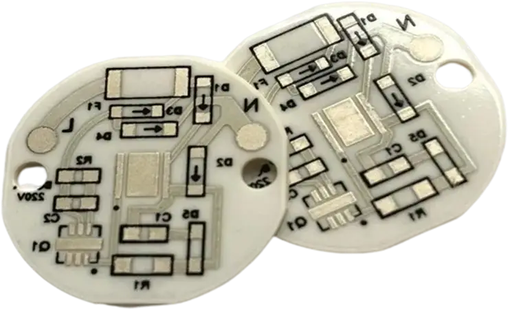
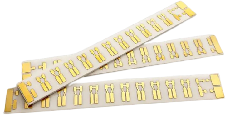
Different Types of Ceramic PCBs Based Upon Manufacturing Processes
When it comes to fabricating ceramic PCBs, the process is a bit more intricate than regular PCBs, but it’s all about achieving superior performance. By blending thermally conductive ceramic powders with organic binders and subjecting the mixture to precise thermal treatments, these PCBs are created to excel in demanding environments. While laser rapid activation (LAM) technology is commonly used, ceramic PCBs are also categorized based on the manufacturing process, each offering unique benefits. Let’s break down the different types of ceramic PCBs based on their fabrication techniques:
1.Thick Film Ceramic Printed Circuit Board
Thick-film ceramic PCBs are manufactured using screen printing, a process that involves applying conductive inks onto the ceramic substrate to form circuit patterns. While this method is well-established, it does come with some challenges. The screen printing method can occasionally result in uneven lines or alignment issues, especially when dealing with intricate circuit designs. As technology progresses, the demand for smaller dimensions and better precision has grown, pushing the boundaries of what can be achieved using thick-film techniques.
Advantages-
●Cost-Effective: Ideal for large-scale production.
●Versatility: Can be used in various applications, from automotive to industrial electronics.
Drawbacks-
●Precision Limitations: As designs become more intricate, maintaining line quality and alignment can become more difficult.
●Size Constraints: The method is more suited for larger dimensions and lower-density circuits.
Example: Thick-film PCBs are often found in automotive electronics, where their cost-effectiveness is a major plus, but also in industrial machinery, where size constraints are not as stringent.
2.Thin Film Ceramic PCB Manufacturing
Thin-film ceramic PCBs are known for their high precision and fine circuit capabilities. These PCBs are made using a process called magnetron sputtering, where a thin copper layer is deposited on a clean ceramic substrate in a vacuum chamber. After the copper layer is applied, a photolithographic process is used to transfer the circuit pattern, followed by etching to remove excess copper. The result is a PCB with highly detailed circuit patterns and smooth surfaces.
Advantages-
●High Precision: The fine circuit resolution makes it ideal for high-frequency and high-performance applications.
●Smooth Surface: The surface quality is excellent, making it suitable for applications requiring low surface roughness.
Drawbacks-
●Expensive Equipment: The manufacturing process requires sophisticated equipment, making it costlier than thick-film techniques.
●Limited to 2D Circuits: Thin-film techniques are unable to produce 3D structures, limiting their application in certain advanced designs.
Manufacturing Process-
●Clean the ceramic substrate to remove impurities.
●Heat the ceramic to evaporate any moisture.
●Apply a thin copper layer using magnetron sputtering.
●Use photolithography and etching to define the circuit pattern.
●Apply a protective solder mask to safeguard the circuit.
3.LTCC (Low-Temperature Co-Fired Ceramic PCB)
LTCC technology allows for the creation of multilayer PCBs that are co-fired at low temperatures, typically between 850-900°C. The key benefit of LTCC is its ability to integrate different materials (such as resistors and capacitors) directly into the PCB structure, providing a compact and reliable solution. With this technology, we can pack more power into a smaller space, making it perfect for applications that demand high functionality without compromising on compactness.
Advantages-
●Multilayer Integration
●High Thermal Conductivity
Drawbacks-
●Complexity: The manufacturing process can be intricate, with a need for precise alignment of layers.
●Shrinkage During Firing: The material undergoes shrinkage during the firing process, which requires careful management of layer alignment.
Example: LTCC is often used in high-performance applications such as medical devices, automotive control systems, and telecommunication modules, where a compact and reliable circuit is needed.
4.HTCC (High-Temperature Co-Fired Ceramic PCB)
HTCC is one of the earliest methods for fabricating ceramic PCBs, and it’s used primarily in high-temperature, high-performance applications. The process involves co-firing ceramic materials (like alumina, mullite, or aluminum nitride) at extremely high temperatures (between 1300°C and 1600°C). The result is a PCB with exceptional mechanical strength, thermal conductivity, and chemical stability. HTCC is ideal for environments that demand durability and precision under extreme conditions.
Advantages-
●Exceptional Durability: With a higher sintering temperature, HTCC provides a robust PCB capable of withstanding extreme environments.
●High Thermal Conductivity: HTCC excels at heat dissipation, making it ideal for power electronics and industrial applications.
Drawbacks:
●High Manufacturing Costs: The high temperatures and specialized materials involved make the HTCC process more expensive than other methods.
●Limited Circuit Conductivity: The process can result in a lower conductivity of the metal traces compared to other types of ceramic PCBs.
Manufacturing Process-
●Ceramic powders are prepared and dried at high temperatures to solidify.
●High-melting-point metals (such as tungsten or molybdenum) are melted and printed onto the substrate to form circuit layers.
●The layers are co-fired at 1500-1600°C, ensuring strong bonding and durability.
●Finally, a solder mask is applied to protect the circuit layers.
Example: HTCC is commonly found in aerospace systems, military electronics, and high-performance automotive components, where reliability under harsh conditions is a must.
Ceramic PCB Types Based on Manufacturing Processes
| Manufacturing Process | Advantages | Drawbacks | Ideal Applications |
| Thick Film | Cost-effective, versatile, suitable for large-scale production | Precision limitations, size constraints | Automotive, industrial machinery |
| Thin Film | High precision, smooth surface | Expensive equipment, limited to 2D circuits | High-frequency circuits, telecommunications, radar |
| LTCC | Multilayer integration, high thermal conductivity | Complexity in manufacturing, shrinkage issues | Medical devices, automotive control systems, telecommunication |
| HTCC | High durability, excellent thermal conductivity | High cost, lower conductivity | Aerospace, military electronics, power electronics |
Ceramic PCB Prototype Delivery Date and Prices
When you’re looking to prototype ceramic PCBs, it’s important to understand both the cost structure and lead time to manage expectations and keep everything on track. Ceramic PCBs are made through a specialized manufacturing process, which brings its own challenges in terms of pricing and time requirements. Knowing what to expect and how to navigate these aspects can help you avoid surprises and ensure everything comes together as planned, whether you’re on a tight budget or schedule. This preparation helps streamline the process, so you can focus on the end result without getting bogged down.
Understanding the Cost of Ceramic PCB Prototypes
The price of ceramic PCBs can vary significantly based on a number of factors. It’s not as simple as just choosing a standard board and waiting for a quote. To get a precise estimate, you’ll need to consider the following:
1.Material Choice: Ceramic substrates come in various materials, each with different costs. For example, alumina, aluminum nitride, and silicon carbide each have unique price points due to their thermal, electrical, and mechanical properties.
2.Board Size and Complexity: Larger ceramic PCBs or those with more complex designs will generally cost more due to the additional labor and materials required to manufacture them. Simple, single-layer designs might cost less, but complex multilayer ceramic PCBs will command a higher price tag.
3.Layer Count: The number of layers involved in the PCB design influences the price. Multilayer ceramic PCBs demand higher precision and more intricate processing, which can increase both cost and manufacturing time.
4.Quantity: The cost per unit typically decreases with larger order quantities. If you’re looking to manufacture ceramic PCBs in bulk, you can often expect a better price per unit as suppliers work more efficiently with larger volumes.
5.Additional Processes: Secondary operations such as etching, solder mask application, and vias drilling can add additional costs to the process. These are typically needed to ensure your design meets the necessary electrical and mechanical specifications.
●Example: A customer submitting a Gerber file for a simple, single-layer ceramic PCB might receive an estimate of $80-$100 per board for small quantities. But if they were to request a multilayer design with a higher thermal conductivity material, the price could jump to $300-$500 per board depending on the complexity.
●Pro Tip: Always ask for a breakdown of costs so that you understand where your money is going. PCB Manufacturers will often charge differently for materials, design, and finishing processes.
Lead Time for Ceramic PCBs: What to Expect
The lead time for manufacturing ceramic PCBs varies quite a bit compared to more common FR4 PCBs made from materials like aluminum. While the standard turnaround for FR4 boards is around 5-7 working days, ceramic PCBs involve a more detailed and intricate process that can take longer.
What Affects Lead Time-
1.Manufacturing Process: Ceramic PCB production involves multiple steps including screen printing, sintering, laser etching, and solder mask application. Each of these steps requires time to ensure quality and precision. Sintering especially is a lengthy process where ceramic layers are fused together in a high-temperature furnace.
2.Board Specifications: Custom shapes, sizes, or multi-layer designs will naturally take more time to manufacture than a basic single-layer board.
3.Order Quantity: Larger orders typically extend lead times due to the increased complexity of producing multiple units, especially when multiple layers or materials are involved.
●Standard Lead Time: The average time for ceramic PCB prototypes typically ranges between 13-15 working days, depending on complexity and order size. This time allows for the necessary steps to ensure that the ceramic boards meet the exact specifications required.
●Expedited Orders: If you’re in a rush, don’t worry! Manufacturers like JarnisTech can accommodate expedited orders, delivering ceramic PCBs in as little as 7 days. This is ideal if you need prototypes quickly for testing or if you’re racing against a tight deadline.
●Example: A technology startup needed to quickly prototype a high-frequency circuit using ceramic PCBs. They placed an expedited order and were able to get a batch of multilayer ceramic PCBs in just 7 days, which was a significant improvement over the usual 15-day turnaround.
What Happens After You Send the Gerber Files?
Once you send your Gerber files to us, you’ll receive a custom quote that includes both the price and lead time for your order. To get an accurate estimate, make sure your Gerber files are detailed and up to spec, including layer stack-up, hole sizes, and any special requirements. A well-prepared Gerber file minimizes the back-and-forth and speeds up the process.
Additional Considerations-
●Prototyping Needs: Prototypes are often smaller batches, and prices can vary widely. If you’re testing out a new design, it’s best to start with a small batch to gauge performance before placing a larger order.
●Design Changes: If changes are made to the design after the initial order, they may extend the lead time or increase costs due to the rework involved. Always ensure that your design is finalized before submitting.
Challenges and Solutions in Ceramic PCB Adoption
The adoption of ceramic PCBs introduces technical, logistical, and financial challenges that require a structured and in-depth approach. These issues range from managing production costs to overcoming design complexity and maintaining supply chain stability, particularly for industries like aerospace, medical technology, and high-performance computing. Below, we delve into specific challenges and provide data-backed solutions, practical tools, and actionable strategies to address them.
Overcoming Cost Barriers in Ceramic PCB Manufacturing
The cost of ceramic PCB production stems from the specialized materials (e.g., aluminum nitride, silicon carbide) and the high-precision processes involved. Unlike traditional PCBs, ceramic PCBs require advanced manufacturing steps such as sintering, laser drilling, and thin-film deposition, which can inflate production costs.
Detailed Cost Analysis and Mitigation Strategies-
| Cost Element | Ceramic PCBs | Standard PCBs | Mitigation Strategy |
| Raw Materials | High: Al₂O₃, Si₃N₄, AlN, SiC | Low: FR4, standard copper | Establish long-term contracts with material suppliers. |
| Fabrication Techniques | Precision-intensive (e.g., DPC) | Standard techniques | Use localized manufacturing to reduce logistics costs. |
| Prototyping | Slower due to complexity | Faster | Adopt 3D printing for rapid prototyping. |
| Scalability | Limited for small batches | Flexible | Opt for batch processing to reduce per-unit costs. |
Case Study: Medical Devices Industry
A medical equipment manufacturer reduced production costs for ceramic PCBs by 20% by integrating Design for Manufacturability (DFM) principles, ensuring that designs aligned with available manufacturing capabilities.
●Insight: While initial production costs can be daunting, optimizing production pipelines, leveraging bulk sourcing, and embracing automation can significantly lower expenses without compromising quality.
Addressing Design Complexity with Advanced Tools
Ceramic PCBs often require designs that accommodate high thermal conductivity, multi-layered circuits, and compact footprints. These demands elevate the need for precision during the design phase, which is why advanced simulation and layout tools are indispensable.
Key Software Tools for Ceramic PCB Design-
| Tool | Features | Best Suited For | Example Applications |
| Altium Designer | Comprehensive PCB layout, 3D visualization, DFM checks | Multi-layer ceramic circuits | Thermal and electrical optimization |
| ANSYS Electronics | Multiphysics simulation for PCBs | High-power applications | Predicting thermal and stress responses |
| Mentor Xpedition | Signal and power integrity analysis | RF and high-frequency designs | Ensuring stability in telecommunication devices |
| COMSOL Multiphysics | Customizable simulations for heat and electromagnetic properties | Advanced material testing | Evaluating thermal conductivity for ceramics |
Advanced Design Example
A telecommunications firm utilized ANSYS to simulate heat dissipation in a ceramic PCB designed for 5G applications. The tool helped optimize copper trace placement, reducing hotspots by 15%.
Ensuring Supply Chain Stability for Critical Industries
The dependence on rare and high-performance materials like beryllium oxide (BeO) and silicon nitride (Si₃N₄) makes supply chain reliability a cornerstone for industries using ceramic PCBs. Disruptions in material availability or manufacturing can lead to project delays, particularly for sectors requiring strict quality standards.
Strategies for Building a Resilient Supply Chain-
| Approach | Advantages | Challenges | Implementation Tips |
| Direct Supplier Agreements | Reduces middleman costs, ensures quality assurance | Requires high-volume commitments | Engage with ISO-certified manufacturers for consistency. |
| Dual Sourcing | Diversifies material supply to mitigate risks | Increases logistical complexity | Identify secondary suppliers in different regions. |
| Local Manufacturing | Reduces transit times and customs delays | Limited to specific geographies | Partner with regional facilities to ensure rapid response. |
Supply Chain Example: Automotive Industry
An EV manufacturer established a dual-sourcing model for aluminum nitride, splitting suppliers across North America and Asia. This approach enabled them to maintain consistent production during a global materials shortage.
●Insight: Proactively securing a diverse supplier base and monitoring material availability can prevent production halts and ensure timely delivery of ceramic PCBs.
Why Choose Us to Become Your Top-Quality Ceramic PCB Maker?
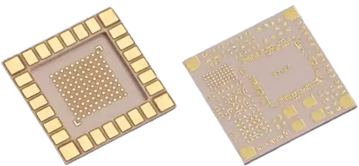
When it comes to selecting a reliable partner for ceramic PCB manufacturing, JarnisTech stands out as one of the leading producers in the industry. We are committed to delivering cutting-edge solutions using advanced techniques like 3D-DPC (Three-Dimensional Direct-Print Circuit) for ceramic PCB production. However, we understand that each customer’s needs are unique, so we also offer a range of other advanced manufacturing techniques to meet specific project requirements. From aluminum nitride PCBs to SiC PCBs, IGBT modules, COB LED modules, and more, JarnisTech is your one-stop services for all things ceramic PCB.
Here’s why you should consider us as your preferred ceramic PCB supplier:
Precision at Every Step
We believe that the key to superior ceramic PCB manufacturing lies in our ability to deliver precision and consistency across all projects.
1.Layer Thickness Customization: We offer customizable layer thickness, ranging from as thin as 1μm to 1mm, depending on your application needs. Whether you need ultra-thin designs for high-frequency circuits or thicker substrates for power electronics, JarnisTech has got you covered.
2.Three-Dimensional Designs: Need a 3D ceramic PCB? No problem. Our advanced 3D-DPC technology allows us to create three-dimensional designs, opening up new possibilities for compact and intricate circuit layouts. This technology is ideal for applications where space is limited, and multi-layer designs are needed to optimize performance.
3.High-Density Capability: With the ability to achieve 20mm minimal line spacing, JarnisTech can handle high-density designs that are crucial for compact electronics. Whether you are designing for 5G networks, automotive electronics, or aerospace systems, we have the expertise and technology to bring your high-density circuit designs to life.
Improved Quality and Durability
When it comes to ceramic PCBs, performance and longevity are non-negotiable. At JarnisTech, we focus on improving both:
1.Temperature Resistance: Our ceramic PCBs are designed to endure extreme temperatures, ensuring reliable performance even in the harshest environments. This heat resistance is key in industries like automotive, aerospace, and high-power systems, where effective thermal management is a must. Whether it’s powering engines or enduring the challenges of space, our ceramic PCBs stand up to the test, ensuring your systems operate without fail in demanding conditions.
2.Welding Quality: The quality of the welding on ceramic PCBs is enhanced with our advanced manufacturing processes, ensuring that connections are secure and reliable under high power conditions. Whether you’re working with high-frequency signals or power modules, we ensure the highest standard of weldability.
3.No Oxide Layer: The absence of an oxide layer on our circuit boards means they have a longer shelf life and improved electrical conductivity. This eliminates the need for extensive cleaning or reworking, making your ceramic PCBs more reliable and reducing maintenance costs over time.
Comprehensive Services and Support
At JarnisTech, we don’t just provide ceramic PCB manufacturing; we offer comprehensive support throughout the entire process.
1.Engineering Support (DFX): We provide one-on-one engineering support for Design for Excellence (DFX), helping optimize your design for manufacturability, reliability, and cost-efficiency. Our experts work closely with your team to address design challenges and provide feedback to improve your project outcomes.
2.Full Range of Products: We offer a wide variety of ceramic PCB products, including but not limited to:
●Aluminum Nitride (AlN) PCBs
●Alumina (Al2O3) PCBs
●Beryllium Oxide (BeO)
●Silicon Carbide (SiC) PCBs
●IGBT Modules
●COB LED and DOB LED Modules
Our Ceramic PCB Manufacturing Capabilities
| Specification | Capability |
| Layer | 1-8 Layers |
| Delivery Time | 1 to 3 Weeks |
| Ceramic Substrates | Al₂O₃ (alumina), SiC, BeO, AlN (aluminum nitride), Si₃N₄ (silicon nitride), Hybrid materials |
| Maximum PCB Size | 138mm × 190mm |
| Finished Board Thickness | 0.25mm, 0.38mm, 0.5mm, 0.76mm, 0.8mm, 1mm, 1.5mm, 2mm |
| Size Tolerance | ≤±50μm |
| Trace Width/Space | 5-10μm: 0.05mm/0.05mm, HOZ: 0.075mm/0.075mm, 1OZ: 0.1mm/0.1mm, 2OZ: 0.127mm/0.127mm, 3OZ: 0.3mm/0.3mm, 6OZ: 0.5mm/0.5mm, 9OZ: 0.6mm/0.6mm |
| Copper Thickness | 2μm to 105μm (DPC), 150μm to 300μm (DBC) |
| Solderability | >95% (IPC-TM-650 2.4.14) |
| Surface Finish | OSP, Immersion Silver, Immersion Gold, Nickel Palladium Gold |
| Laser Drill | ≥75μm |
Let’s Get Started!
Ready to take your ceramic PCB projects to the next level? At JarnisTech, we’re committed to helping you design, manufacture, and assemble the perfect ceramic PCBs for your needs. From initial consultation to final delivery, we’re here to make sure your project runs smoothly and efficiently.
Contact us today to discuss your needs, get a personalized quote, and explore how we can assist you with cutting-edge ceramic PCB manufacturing solutions. Whether you need prototype production, small batches, or large-scale manufacturing, we’re equipped to handle it all. Let’s build something amazing together!
Ceramic PCB Frequently Asked Questions (FAQ)
How does ceramic PCB compare to metal-core PCBs in heat dissipation?
Ceramic PCBs, especially those made with aluminum nitride (AlN), outperform metal-core PCBs in thermal conductivity, providing a more efficient solution for high-power applications.
Can ceramic PCBs support multi-layer designs?
Yes, ceramic PCBs can support multi-layer configurations. However, achieving multiple layers often involves specialized manufacturing techniques like low-temperature co-fired ceramics (LTCC) or high-temperature co-fired ceramics (HTCC).
What surface finishes are available for ceramic PCBs?
Common surface finishes for ceramic PCBs include immersion gold, immersion silver, nickel palladium gold, and organic solderability preservative (OSP), tailored to application-specific requirements.
Are ceramic PCBs environmentally friendly?
Many ceramic PCBs are considered environmentally friendly as they do not involve harmful organic materials and are RoHS-compliant. Some ceramic materials are also recyclable, reducing their environmental impact.
What are the common challenges in soldering ceramic PCBs?
Soldering ceramic PCBs can be challenging due to their high thermal conductivity, which may require precise temperature control. Using solder pastes designed for high-heat applications is recommended.
How do ceramic PCBs handle electrical insulation?
Ceramic materials like alumina (Al₂O₃) and silicon nitride (Si₃N₄) provide excellent electrical insulation while maintaining high thermal conductivity, making them suitable for high-voltage applications.
What is the maximum size of a ceramic PCB that can be manufactured?
Most manufacturers can produce ceramic PCBs up to a size of approximately 138mm × 190mm. Larger sizes may require advanced techniques or custom solutions.


