
Manufacturing multilayer ceramic PCBs demands a high level of expertise and precision. These intricate circuit boards are the driving force behind a wide range of modern technology, from smartphones to satellites. The creation of ceramic PCBs marks a significant achievement in the field of electronics manufacturing, pushing the boundaries of what’s possible in today’s tech landscape.
Multilayer ceramic PCBs are constructed by stacking ceramic substrates, each separated by conductive patterns and insulating layers. To successfully produce these boards, we need to tackle a variety of tasks — from selecting the appropriate materials to ensuring the layers are properly aligned, from drilling vias to controlling the firing process. While ceramic materials offer exceptional electrical and thermal properties, their inherent brittleness, high hardness, and susceptibility to thermal expansion pose challenges that can complicate the production process.
Despite these hurdles, the value of multilayer ceramic PCBs is clear. They’re prized for their outstanding performance in high-frequency applications, their ability to handle substantial power, and their efficient heat dissipation. For us, meeting the demands of smaller sizes, dense interconnections, and advanced electronics means navigating these challenges head-on. By mastering the complexities of ceramic PCB fabrication, we can provide reliable solutions that meet the ever-changing needs of the electronics sector, ensuring that our products keep pace with the industry’s rapid advancements.
The Science and Technology Behind Multilayer Ceramic PCBs
Multilayer Ceramic PCBs are revolutionizing industries with their unique ability to withstand tough environments and demanding applications. These boards rely on ceramic substrates that are capable of handling extreme temperatures, managing power loads, and performing well under high-frequency conditions. Compared to traditional PCBs made of fiberglass or plastic, ceramic PCBs stand out due to their exceptional thermal and electrical performance. They’re built for precision, energy efficiency, and durability—making them a go-to solution in industries ranging from automotive to aerospace and telecommunications.
How Multilayer Ceramic PCBs Are Different from Traditional PCBs?
When you stack Multilayer Ceramic PCBs against the usual fiberglass or plastic-based PCBs, the differences are immediately clear. Traditional PCBs usually rely on copper traces over a fiberglass base, which works well for many applications but falls short in more demanding environments. In contrast, ceramic PCBs use materials designed to handle higher performance under extreme conditions, such as high heat or high-power needs. Here’s what sets them apart:
●Heat Dissipation: Ceramic substrates are much better at dissipating heat compared to traditional PCB materials. With their ability to manage temperature better, ceramic substrates make sure things stay in check, even when the heat is on.
●Electrical Insulation: Ceramic materials are known for their excellent dielectric properties. This means they can handle high-frequency signals, which makes them the right choice for industries like telecommunications and radar systems.
●Durability: Ceramic is incredibly robust. Unlike fiberglass PCBs that can break or wear out, ceramic PCBs are tough enough to resist mechanical stress, vibrations, and harsh environmental conditions.
So, if you’re looking for a PCB that can take the heat (literally) and handle the pressure, ceramic PCBs have your back.
The Impact of Ceramic Substrates on High-Power and High-Frequency Electronics
As industries push the envelope in high-power and high-frequency applications, ceramic substrates have become indispensable. Take power amplifiers or electric vehicle systems, for instance. These systems generate substantial amounts of heat, and traditional PCBs simply can’t keep up. That’s where ceramic PCBs come in, offering better heat management that helps keep the components working properly without the risk of overheating or premature failure.
When it comes to high-frequency performance, ceramic PCBs hold an edge. In industries like satellite communications, telecommunications, and aerospace, managing fast frequencies without compromising signal integrity is no easy task. Ceramic PCBs handle these challenges with ease, providing consistent, reliable performance while preventing signal loss or distortion.
Understanding Dielectric and Conductive Layers in Ceramic PCBs
The design of a Multilayer Ceramic PCB is more than just stacking layers together. It’s all about combining conductive and dielectric materials in ways that optimize performance, making them more efficient and reliable.
●Dielectric Layers: These layers are commonly constructed from ceramics such as aluminum oxide or beryllium oxide. They provide insulation to the PCB while effectively managing electrical signals by reducing interference. On top of that, these materials are known for their excellent thermal conductivity, helping to maintain optimal temperatures even under demanding, high-power scenarios.
●Conductive Layers: These are typically made of copper and are patterned onto the ceramic surface. The copper traces serve as the pathways for electrical current to travel, ensuring the PCB performs its intended function.
Key Manufacturing Techniques for Multilayer Ceramic PCBs
When it comes to manufacturing Multilayer Ceramic PCBs, the process must be tailored to meet the specific demands of each application. Whether it’s for electric vehicles, aerospace, or telecommunications, a solid understanding of the right techniques is necessary. Two popular methods used for ceramic PCB production are HTCC (High-Temperature Co-Fired Ceramics) and LTCC (Low-Temperature Co-Fired Ceramics). Each process offers distinct characteristics that make them better suited for particular industries or uses.
Let’s dive into the two main processes and explore how they work, their differences, and which one might be best suited for your project.
HTCC and LTCC Manufacturing Processes for Multilayer Ceramic PCBs
What are HTCC and LTCC-
The HTCC (High-Temperature Co-Fired Ceramics) process is used to create ceramic PCBs that operate in high-temperature environments. The HTCC method involves the use of high-temperature cofiring to bond ceramic and metal layers into a single, integrated board. This process typically occurs at temperatures above 1,500°C and is best suited for applications that require higher thermal conductivity and the ability to operate under extreme conditions. HTCC is most commonly used in industries such as aerospace, power electronics, and automotive systems.
On the other hand, LTCC (Low-Temperature Co-Fired Ceramics) involves a lower firing temperature (around 850°C to 900°C). The LTCC process enables the use of a broader range of materials for both the ceramic substrate and the conductive layers, including silver, gold, and palladium. LTCC is especially popular in telecommunications and medical device applications due to its ability to achieve higher density designs and support multilayer architectures with greater ease.
Differences Between HTCC and LTCC-
While both processes co-fire ceramic and metal layers, the temperatures and material types they use vary significantly, which affects their properties and applications.
●Temperature: HTCC uses much higher temperatures (above 1,500°C) compared to LTCC, which operates at lower temperatures (850°C-900°C).
●Material Choices: HTCC typically uses more rigid, stable ceramic materials like alumina, while LTCC offers more flexibility with materials such as glass ceramics that are suitable for lower temperature processes.
●Applications: HTCC works well in environments that demand superior thermal management, such as high-power electronics, where heat dissipation is a must. On the other hand, LTCC is better suited for situations where compact design and efficient signal handling are necessary, like in communication systems that require precise and reliable signal processing.
Choosing the Right Manufacturing Process for Multilayer Ceramic PCBs-
When selecting between HTCC and LTCC for your project, the primary factors to consider are the operating environment, required thermal conductivity, and the need for high-frequency performance.
●High-Power Applications: HTCC is often the better choice for designs where high power is involved, such as in power modules for electric vehicles or aerospace electronics.
●Miniaturized Devices: If you’re designing devices that need to be compact without compromising on signal clarity, LTCC may be your best bet. It’s widely used in communication and medical applications where space constraints and signal integrity are a must.
The Co-Firing Process in Multilayer Ceramic PCB Production
The co-firing process is the foundation of both HTCC and LTCC production. In simple terms, co-firing refers to the process of firing multiple layers of ceramic and metal together in a single step, allowing the layers to bond seamlessly. This method ensures that the different layers work together as a cohesive unit, which is essential for high-performance electronic components.
The Co-Firing Process Explained-
During co-firing, the ceramic and metal materials are carefully stacked into layers, each serving a specific purpose. The ceramic materials form the base of the PCB, while metal layers act as the conductive pathways for electrical signals. These layers are fired together in a kiln, which causes them to fuse, forming a single piece of material.
The temperature and time required for co-firing vary depending on the type of ceramic and metal being used. For example, with HTCC, the process occurs at much higher temperatures, which results in a strong bond that can withstand harsh conditions.
Challenges in Co-Firing Multilayer Ceramic PCBs-
While co-firing offers many advantages, it also comes with its share of challenges. One of the biggest challenges is ensuring that all the materials used in the process have compatible thermal expansion rates. If the materials expand or contract at different rates during the firing process, it can lead to warping or cracking of the PCB. This is a particular concern in high-temperature applications, where the risk of thermal stress is higher.
Another issue in co-firing is material compatibility. Not all materials can be co-fired together, especially when using multiple layers with different compositions. Therefore, we need to carefully select materials that work well together to avoid issues like delamination or signal degradation.
Optimizing the Co-Firing Process for High-Power Applications-
In high-power applications, the stakes are even higher. To meet the rigorous demands of power electronics, the co-firing process must be fine-tuned to handle the increased thermal loads. This requires selecting materials that offer high thermal conductivity and low thermal expansion to reduce the risk of warping. Additionally, advanced firing techniques, such as slow ramp-up and ramp-down procedures, are employed to ensure that the ceramic PCB can handle the thermal stresses during the firing process.
Advanced Manufacturing Techniques for Multilayer Ceramic PCBs
Manufacturing Multilayer Ceramic PCBs is not just about traditional methods—there are several advanced techniques that are being used to improve performance and increase the efficiency of the process. Here are some of the cutting-edge methods being employed:
Laser Direct Structuring for Multilayer Ceramic PCBs-
Laser Direct Structuring (LDS) is a process that uses laser technology to directly pattern the conductive traces onto the ceramic substrate. This method is especially beneficial for creating complex, high-density designs that would be difficult or impossible to achieve with traditional methods. By using a laser to etch intricate patterns directly onto the ceramic, we can produce smaller, more efficient circuits without the need for additional process steps like chemical etching. LDS technology is often used in consumer electronics and automotive systems, where space and performance are at a premium.
Thin Film Deposition in Multilayer Ceramic PCB Production-
Thin-film deposition is another advanced technique used to create high-density ceramic PCBs. In this process, extremely thin layers of conductive material (like copper or silver) are deposited onto the ceramic substrate using physical vapor deposition (PVD) or chemical vapor deposition (CVD) methods. This technique is particularly useful in high-frequency applications where precision is required. The thin-film method allows for the creation of fine traces with minimal space, making it suitable for devices that require compact designs and high performance.
Automation in Multilayer Ceramic PCB Manufacturing-
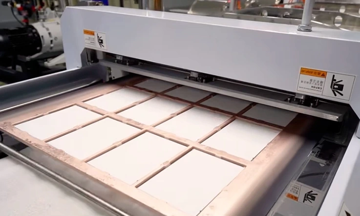
Automation is transforming the manufacturing process for Multilayer Ceramic PCBs. By using automated machines for processes like material handling, printing, and firing, we can achieve higher precision, faster production times, and greater scalability. Automation reduces human error, increases consistency, and lowers costs in the long run. In high-volume production environments, automation helps meet the growing demand for ceramic PCBs while maintaining high-quality standards.
Overcoming the Challenges in Manufacturing Multilayer Ceramic PCBs
When manufacturing Multilayer Ceramic PCBs, various challenges arise, ranging from material selection to the precision of manufacturing processes. The production of these advanced electronic components requires a balanced approach that combines state-of-the-art technology, precise methods, and careful process control. Here’s how manufacturers can navigate these obstacles and ensure the production of high-performance ceramic PCBs.
Advanced Material Characterization and Selection
The durability and effectiveness of any ceramic PCB rely heavily on selecting the right materials. With a wide variety of ceramic substrates available, each suited for particular applications, thorough material assessment is needed to evaluate their thermal, mechanical, and electrical properties. This ensures that the chosen material will perform well across different environments and meet the demands of specific systems.
Material Evaluation Techniques-
Advanced material characterization methods such as X-ray diffraction (XRD), scanning electron microscopy (SEM), and energy dispersive X-ray spectroscopy (EDS) are used to evaluate the crystalline structure, surface quality, and chemical composition of ceramic materials. These analyses help in determining how well the material will perform under electrical and thermal stress.
| Material Type | Dielectric Constant | Thermal Conductivity (W/mK) | Applications |
| Aluminum Oxide (Al₂O₃) | 9-10 | 30-35 | Power electronics, automotive |
| Silicon Nitride (Si₃N₄) | 5-7 | 140-180 | High-power and high-temperature systems |
Material Selection Criteria-
Choosing materials that are well-suited to the specific requirements of the PCB application can help reduce manufacturing difficulties. Factors such as dielectric loss, high-temperature resistance, and machinability need to be factored into material selection. For example, Aluminum Nitride (AlN) is often selected for its excellent thermal conductivity, making it better for high-power applications.
Precision Equipment and Process Control
Manufacturing Multilayer Ceramic PCBs requires the use of precise equipment to achieve accurate dimensions and tolerances. The complexities of handling multiple layers with ceramic materials necessitate the use of specialized machinery and process control measures.
Precision Laser Drilling and Patterning-
Ceramic PCBs need precise via formation, which is often accomplished through methods like laser drilling and laser patterning. Laser drilling stands out for its ability to deliver pinpoint accuracy while keeping heat-affected zones to a minimum. This is particularly helpful when working with ceramics, ensuring that the vias are cleanly formed without causing damage to the material.
| Equipment Type | Application | Key Benefits |
| Laser Drilling | Via formation in multilayer PCBs | High precision, minimal material stress |
| Laser Patterning | Surface patterning for circuit traces | Fine lines and precise trace patterns |
Advanced Alignment and Bonding-
During the lamination process, layers need to be aligned with high precision to guarantee proper electrical connectivity. Alignment equipment is designed to meet tight tolerances, ensuring that each layer lines up exactly, reducing the risk of misalignment, which could affect the PCB’s functionality. Bonding methods like ultrasonic bonding or epoxy bonding are applied to securely attach the layers while maintaining the ceramic’s structural integrity.
Firing and Sintering Control-
The firing stage in ceramic PCB production requires precise temperature management to achieve the desired material properties. Proper control over the sintering process is necessary to avoid defects like cracking, warping, or inconsistent shrinkage. Accurate temperature gradients ensure the ceramic materials bond and solidify effectively, leading to a durable and reliable final product.
In-Process Inspection and Quality Control
Throughout the manufacturing process, continuous inspection helps catch defects early and maintain a high-quality product. Advanced techniques, such as automated optical inspection or X-ray imaging, monitor various parameters, ensuring that every step of production sticks to required standards, preventing issues that could affect the final output.
Optical Inspection and Electrical Testing-
Optical inspection techniques, including automated optical inspection (AOI), help detect visible defects such as misalignments or contamination. Electrical testing methods such as impedance testing and continuity checks verify that the multilayer connections meet the required electrical standards.
| Inspection Type | Technique Used | Purpose |
| Optical Inspection | Automated Optical Inspection (AOI) | Detect surface-level defects or misalignments |
| Electrical Testing | Impedance & Continuity Testing | Verify proper electrical performance |
Statistical Process Control (SPC)-
Statistical methods are applied to monitor and control the manufacturing process. By analyzing data from different stages of production, we can identify patterns and address issues before they become critical, thereby improving yield rates and consistency.
Specialized Manufacturing Techniques
When traditional methods are insufficient, specialized techniques come into play. These methods help ensure the PCB meets stringent performance requirements while maintaining reliability and cost-effectiveness.
Laser Micromachining for Precision Patterning-
Laser micromachining is employed for ultra-precise patterning on ceramic substrates, enabling the creation of fine traces and intricate designs. The technology reduces material waste and ensures that the patterns remain accurate, even with complex geometries.
Ultrasonic Bonding and Wire Bonding-
For ensuring reliable electrical connections, ultrasonic bonding or wire bonding can be used. These methods are particularly effective for ceramic substrates, which require low temperatures to avoid damage during the bonding process. These techniques help achieve strong, long-lasting bonds between components.
Collaboration and Innovation
Manufacturers of Multilayer Ceramic PCBs can stay ahead of challenges by collaborating with material suppliers and equipment manufacturers to develop cutting-edge solutions. Joint research and development initiatives are a powerful way to continuously improve manufacturing processes and introduce innovative materials.
Research and Development Investment-
Investing in R&D helps improve the manufacturing process, reduce costs, and improve overall product quality. Manufacturers who stay at the forefront of technological developments can enhance their manufacturing capabilities, ensuring that their Multilayer Ceramic PCBs can meet the evolving demands of industries like automotive, industrial equipment, and power electronics.
| Collaboration Type | Example | Benefit |
| Material Innovation | Working with suppliers to test new ceramics | Improved thermal and electrical properties |
| Process Development | Partnering with equipment manufacturers for precision tooling | Enhanced accuracy, reduced defects |
Critical Design Considerations for Multilayer Ceramic PCBs
When designing Multilayer Ceramic PCBs, there are several aspects to consider to ensure the final product meets the demands of high-frequency, high-power, and long-term durability. The design must account for signal integrity, thermal management, material selection, and long-term performance. Every design decision impacts the final functionality and reliability, and thus, careful planning is essential to ensure that each layer works seamlessly with the others to achieve the desired performance.
Next, we will explore the core design areas that need to be addressed: high-frequency performance, thermal management, and reliability.
Designing Multilayer Ceramic PCBs for High-Frequency Performance
The performance of Multilayer Ceramic PCBs in high-frequency applications directly affects signal clarity and transmission efficiency. High-frequency circuit designs require low signal attenuation and optimal electrical properties. To achieve this, we must implement measures to maintain signal integrity and ensure stable signal transmission within the circuit.
Signal integrity is a big deal in high-frequency applications, where even a little noise or interference can mess up the signals. During the design phase, choosing the right ceramic materials with the proper dielectric constant helps keep signal loss in check as they travel through the circuit, ensuring the signals stay sharp and clear. This careful selection keeps your design from getting bogged down by unwanted noise, keeping everything running smooth.
Impedance Control in Multilayer Ceramic PCBs-
Impedance control is a fundamental aspect of high-frequency designs. To minimize signal reflections and interference, our designers need to ensure consistent impedance along every signal path in the PCB. Multilayer Ceramic PCBs achieve this by carefully designing the electrical properties of each layer and material used. Proper impedance control ensures that signals travel without distortion and reduces performance degradation caused by signal mismatching.
| Material | Impedance Control (Ω) | Dielectric Constant | Signal Loss (dB/cm) |
| Aluminum Oxide (Al2O3) | 50 | 9.8 | 0.2 |
| Silicon Nitride (Si3N4) | 75 | 7.0 | 0.18 |
| Aluminum Nitride (AlN) | 55 | 8.0 | 0.15 |
Minimizing Signal Loss in Multilayer Ceramic PCBs-
Minimizing signal loss is another challenge in high-frequency designs. Ceramic substrates, with their superior electrical and thermal properties, can effectively reduce signal loss. By selecting low-loss materials, optimizing circuit layouts, and adjusting the routing of signals, we can significantly cut down on attenuation.
| Design Element | Signal Loss Reduction (%) | Suggested Approach |
| Material Selection | 20 | Use high-purity ceramics |
| Trace Width | 15 | Increase trace width for lower loss |
| Layer Configuration | 10 | Optimize signal routing to minimize loss |
Thermal Management in Multilayer Ceramic PCBs for High-Power Applications
Thermal management is a significant challenge in high-power applications. As power demands increase, electronic components generate substantial heat, which must be dissipated effectively to prevent overheating and performance degradation. Ceramic materials are reliable for high-power applications due to their superior thermal conductivity, which helps quickly transfer heat and maintain the stability of the PCB.
Why Thermal Management is Crucial in High-Power Multilayer Ceramic PCBs-
In high-power applications, such as electric vehicles and power amplifiers, heat buildup is one of the primary factors affecting system stability. Multilayer Ceramic PCBs offer excellent thermal conductivity, allowing them to efficiently transfer heat to heat sinks or the external environment, preventing temperature rise that could lead to circuit failure. During the design phase, it is important to plan the circuit layout to ensure heat is evenly distributed.
Thermal Conductivity of Multilayer Ceramic PCBs-
The thermal conductivity of ceramic materials is one of the main reasons why Multilayer Ceramic PCBs excel in high-power applications. For instance, Aluminum Nitride (AlN) and Silicon Carbide (SiC) have thermal conductivities far higher than conventional FR4 materials, enabling them to dissipate heat more effectively.
| Material | Thermal Conductivity (W/mK) |
| Aluminum Oxide (Al2O3) | 28 |
| Aluminum Nitride (AlN) | 180 |
| Silicon Carbide (SiC) | 490 |
Cooling Strategies for High-Power Multilayer Ceramic PCBs-
When it comes to high-power applications, effective heat management is a must. Different methods, such as natural convection, forced air cooling, and liquid cooling, are commonly used depending on the job at hand. Picking the right cooling method for the situation not only ramps up thermal efficiency but also helps the PCB go the distance.
| Cooling Method | Effectiveness | Suitable Applications |
| Natural Convection | Moderate | Low-power devices |
| Forced Air Cooling | High | Power supplies |
| Liquid Cooling | Very High | Electric vehicles |
Designing Multilayer Ceramic PCBs for Reliability and Durability
In high-power and high-frequency applications, Multilayer Ceramic PCBs need to stand the test of time. The selection of materials, their ability to adapt to varying environments, and rigorous testing protocols are crucial to making sure the PCB keeps going strong. By refining the design, these PCBs can not only last longer but also keep doing their job effectively, even in tough conditions. Proper planning and design tweaks can ensure that they’re up to the task, no matter how demanding the environment gets.
Material Selection for Durability in Multilayer Ceramic PCBs-
The material chosen for Multilayer Ceramic PCBs plays a direct role in the PCB’s durability and longevity. Selecting materials with high compressive strength, thermal stability, and good corrosion resistance can significantly improve the PCB’s reliability. For example, Aluminum Nitride (AlN) and Silicon Carbide (SiC) are commonly used in high-temperature and high-power environments due to their durability.
Vibration Resistance in Multilayer Ceramic PCBs-
Multilayer Ceramic PCBs must also withstand vibration and shock, especially in automotive, aerospace, and industrial applications. Compared to traditional substrate materials, ceramic materials are more resistant to vibrations, which helps maintain the integrity of the circuit and prevents failure in challenging environments.
Environmental Stress Testing for Multilayer Ceramic PCBs-
Environmental stress testing is essential to evaluate the long-term reliability of Multilayer Ceramic PCBs. These tests, which include exposure to high temperature, humidity, thermal cycling, and mechanical shock, help ensure the PCB can withstand harsh environmental conditions and continue functioning over time. These tests also allow us to assess the material’s performance and make any necessary adjustments to the design.
| Test Type | Conditions | Purpose |
| High Temperature Test | 150°C, 1000 hours | Test material stability |
| Vibration Test | 10g, 20-2000Hz | Evaluate shock resistance |
| Thermal Cycling | -55°C to +125°C | Assess thermal stress |
Performance Characteristics and Applications of Multilayer Ceramic PCBs
Multilayer Ceramic PCBs have emerged as a reliable solution for demanding applications across various industries due to their exceptional performance in terms of power handling, heat dissipation, and mechanical strength. These properties make them a prime choice in fields like power electronics, automotive electronics, and industrial systems. Their ability to maintain performance under extreme conditions makes them a solid option for electronics in high-power environments, where heat and voltage stress are prevalent.
High-Power Handling with Multilayer Ceramic PCBs
In the world of high-power systems, the ability to handle large currents and dissipate heat effectively is a top consideration. Multilayer Ceramic PCBs are designed to excel in these areas, providing reliable performance in power electronics and related fields. By integrating materials with high thermal conductivity and low electrical resistance, these PCBs support the smooth operation of high-power systems while maintaining stability and efficiency.
Multilayer Ceramic PCBs in Power Electronics-
Power electronics require robust materials that can support high current levels while effectively managing heat. Multilayer Ceramic PCBs stand out in these applications, as they can handle significant power without compromising the functionality of surrounding components. These boards are integral in systems such as power supplies, amplifiers, and converters, where high current and voltage levels are the norm.
Advantages of Multilayer Ceramic PCBs for High-Power Systems-
For systems dealing with high power, the advantages of Multilayer Ceramic PCBs are immediately apparent. Their superior thermal management capabilities enable them to dissipate heat more efficiently than other materials, ensuring the stability and longevity of sensitive components. Additionally, their resistance to high temperatures makes them an excellent fit for environments where heat would normally degrade traditional PCB materials.
Multilayer Ceramic PCBs for Automotive Power Systems-
In automotive applications, especially in electric vehicles (EVs), Multilayer Ceramic PCBs manage power control and energy distribution across various systems, such as battery management systems (BMS) and motor control units (MCUs). These PCBs handle high power loads while withstanding thermal and mechanical stress, contributing to the consistent operation of EVs, even under demanding conditions. Their stable performance ensures that systems remain efficient, even during challenging driving situations.
Multilayer Ceramic PCBs in Automotive Electronics
The automotive industry increasingly relies on advanced electronics to enhance performance, safety, and efficiency. Multilayer Ceramic PCBs are a preferred material in automotive electronics due to their high durability and reliability under extreme conditions. These PCBs are essential components in systems ranging from electric vehicle powertrains to advanced driver-assistance systems (ADAS), where precision and resilience are required.
Applications in Electric Vehicles (EVs)-
In EVs, Multilayer Ceramic PCBs are core to managing the power and control of various subsystems, including energy storage, motor control, and power distribution. These PCBs ensure efficient communication between components, supporting high-performance operations in battery management systems and powertrain electronics.The reliable thermal performance of ceramic PCBs helps maintain stability, even under high loads. With ceramic PCBs, EVs operate efficiently, even in demanding conditions.
Reliability of Multilayer Ceramic PCBs in Automotive Environments-
Automotive environments are subject to fluctuating temperatures, vibrations, and other stresses that can degrade traditional PCB materials over time. Multilayer Ceramic PCBs, with their robust construction and resistance to thermal cycling and mechanical shock, offer superior reliability. This makes them ideal for use in automotive environments, where maintaining performance over extended periods is a main factor for system longevity.
Advanced Driver-Assistance Systems (ADAS) and Multilayer Ceramic PCBs-
ADAS technology, which includes sensor systems like radar and LiDAR, requires high-speed data transmission and processing. Multilayer Ceramic PCBs are increasingly utilized in these systems, as they provide a stable foundation for handling the complex electronic components involved. Their low loss characteristics and high thermal conductivity make them suitable for the performance demands of ADAS, contributing to the overall safety and functionality of modern vehicles.
Multilayer Ceramic PCBs in Industrial Equipment
Industrial equipment often works in environments that demand solid power handling and unwavering reliability. Multilayer Ceramic PCBs step up to the plate, offering durable solutions that can handle high power levels and tough conditions. These PCBs are increasingly being utilized in industrial settings like automation systems, motors, and power electronics. Their design and capabilities help ensure that these systems perform efficiently, even when the conditions are less than ideal.
High-Power Equipment and Multilayer Ceramic PCBs-
Industrial equipment such as large motors and power inverters requires components that can manage high power without overheating or degrading. Multilayer Ceramic PCBs are highly suitable for these applications, as their exceptional heat dissipation properties allow them to maintain optimal operating temperatures even under heavy loads. This helps prevent equipment failure and extends the lifespan of critical components.
Applications in High-Voltage Systems-
In high-voltage industrial applications, Multilayer Ceramic PCBs offer the insulation and voltage capacity needed for smooth and secure operation. These boards are widely used in systems like power distribution units, high-voltage transformers, and energy storage devices, where they must handle electrical stress without risking failure. Thanks to their strong electrical insulation and heat resistance, these PCBs are built to hold up under pressure, making them perfect for demanding, high-energy environments.
Multilayer Ceramic PCBs for Reliability in Harsh Conditions-
Industries such as manufacturing, mining, and chemical processing demand equipment that can withstand extreme conditions. Multilayer Ceramic PCBs, with their resistance to environmental stress factors such as temperature fluctuations, moisture, and dust, are built to perform in these tough environments. This durability ensures that industrial systems remain operational in challenging settings, where downtime can have costly consequences.
Reliability and Testing of Multilayer Ceramic PCBs
The process of ensuring the durability and functionality of Multilayer Ceramic PCBs involves rigorous testing and validation. These PCBs must endure various conditions that are commonly encountered in high-power, automotive, and industrial applications. The reliability of these components directly influences their performance and lifespan, making testing a fundamental part of the design and manufacturing phases. Below, we examine several essential aspects of reliability and the testing protocols that confirm these PCBs are suited for their intended applications.
Reliability Factors in Multilayer Ceramic PCB Design
Designing Multilayer Ceramic PCBs for reliability calls for a strategic approach to material selection and stress resistance. The right materials directly influence the long-term performance of the PCB, particularly in environments subject to heavy mechanical stress, constant vibrations, and fluctuating temperatures.
Material Durability in Ceramic PCB Designs-
The choice of materials such as Aluminum Oxide (Al₂O₃) and Silicon Nitride (Si₃N₄) directly impacts the durability of the ceramic PCB. These materials are well-regarded for their resistance to high temperatures, corrosion, and mechanical stress, ensuring the longevity and consistent performance of the PCB in demanding environments.
| Material | Thermal Conductivity (W/mK) | Mechanical Strength (MPa) | Applications |
| Aluminum Oxide | 30-35 | 320-380 | Power electronics, automotive |
| Silicon Nitride | 140-180 | 1000-1200 | High-power and high-temperature systems |
Mechanical Stress and Vibration Resistance Testing-
Testing Multilayer Ceramic PCBs for mechanical stress and vibration ensures that they can withstand external forces without failure. These tests simulate real-world conditions where the PCB is exposed to shock, vibration, and temperature changes, which are common in automotive and industrial environments.
| Test Type | Test Method | Performance Requirements |
| Vibration Testing | Simulated mechanical shocks and vibrations | PCB must resist cracks or component detachment |
| Thermal Cycling | Exposure to rapid temperature changes | No delamination or material degradation |
Long-Term Testing for Automotive and Industrial Applications-
For high-power applications, testing becomes even more necessary to ensure Multilayer Ceramic PCBs stand up to demanding conditions. These PCBs must handle increased current, higher thermal stresses, and more challenging environments, all while maintaining stable performance.
| Testing Duration | Test Environment | Pass Criteria |
| 1000+ hours | High temperature, humidity, and mechanical stress | No significant performance degradation, no physical failures |
Testing and Validation for High-Power Ceramic PCBs
For high-power applications, testing becomes even more necessary to ensure Multilayer Ceramic PCBs stand up to demanding conditions. These PCBs must handle increased current, higher thermal stresses, and more challenging environments, all while maintaining stable performance.
Thermal Cycling Tests for High-Power Ceramic PCBs-
Thermal cycling tests subject the ceramic PCBs to a range of temperatures to simulate the effects of repeated heating and cooling cycles. This ensures the PCB can withstand the stresses caused by temperature fluctuations without damage.
| Cycle Count | Temperature Range (°C) | Test Duration | Expected Outcome |
| 500 | -40 to 125 | 10-15 hours | No cracking, delamination, or component failure |
Electrical Performance Testing for Multilayer Ceramic PCBs-
Various electrical tests, including impedance and signal integrity tests, are performed to assess the PCB’s capability to handle high-frequency signals and ensure it meets the required electrical specifications.
| Test Type | Test Method | Purpose |
| Impedance Testing | Measure the impedance across different frequencies | Ensure controlled impedance for high-speed signal transmission |
| Signal Integrity Test | Analyze signal reflections and attenuation | Confirm minimal signal loss and interference |
Environmental and Reliability Testing for Power Systems-
Power systems often operate under harsh conditions, so testing for exposure to high humidity, dust, and extreme temperatures is necessary. These tests confirm that the ceramic PCBs can endure these conditions without failing or deteriorating.
| Environmental Factor | Test Conditions | PCB Performance Requirements |
| Humidity | Exposure to 85% RH at 85°C | No degradation or functional issues |
| Dust/Corrosion | Exposure to industrial dust and moisture | No short-circuiting or performance loss |
Accelerated Testing for High-Current Multilayer Ceramic PCBs
High-current applications demand PCBs that are not only functional but reliable over the long term. Accelerated testing helps determine the anticipated performance of these PCBs in a shorter time frame.
Accelerated Life Testing for Ceramic PCBs-
Accelerated life testing exposes the PCB to extreme conditions that simulate years of wear in a much shorter time. This method helps predict the overall lifespan of the ceramic PCB, ensuring it can meet the durability requirements of high-current systems.
| Test Conditions | Duration | Key Indicators to Measure |
| High temperature & load | 1000+ hours | PCB integrity, solder joint strength |
| Extended high-current exposure | 500+ hours | Electrical performance, material degradation |
Environmental Stress Screening for Multilayer Ceramic PCBs-
Environmental stress screening (ESS) helps identify potential weaknesses in the ceramic PCBs before they are deployed in high-current systems. This process subjects the PCBs to a variety of harsh conditions to ensure their durability.
| Test Type | Test Method | Criteria for Passing |
| Stress Screening | Subjecting the PCB to high temperature, vibration, and humidity | No physical or electrical failures |
Failure Mode Analysis of Multilayer Ceramic PCBs-
Failure mode analysis helps us identify the reasons behind any PCB failures. This analysis assists in improving design and manufacturing processes to avoid common failure points in future productions.
| Failure Mode | Potential Cause | Mitigation Strategy |
| Thermal Cycling Failure | Expansion/contraction causing cracks | Use materials with lower thermal expansion coefficients |
| Mechanical Failure | Vibration or shock-induced damage | Strengthen PCB materials and improve manufacturing processes |
Why Choose JarnisTech?
Leading Multilayer Ceramic PCB Manufacturer and Supplier in China
Choosing the right manufacturer for your multilayer ceramic PCBs is a big decision. At JarnisTech, we recognize that this choice impacts your product’s performance and overall success. Here’s why we’re the best option for your project:
1.Expertise and Experience
Choosing a manufacturer with the right expertise can make all the difference. With years of experience in multi-layer ceramic PCB production, we bring a wealth of knowledge to the table. From advanced manufacturing techniques to staying ahead with the latest industry standards, we’ve got the know-how to ensure your PCBs perform at their best.
2.Quality Control and Testing
Our quality control process isn’t just a box we check; it’s integrated throughout production. With a meticulous approach, we carry out a range of tests, including electrical tests, visual inspections, and thermal cycling. Whether it’s impedance analysis or stress testing, we’ve got the tools and expertise to ensure your ceramic PCBs meet the highest standards.
3.Material Sourcing and Traceability
We’re all about using the best materials for your project. We source only from trusted suppliers, keeping a close eye on the entire supply chain. This level of traceability ensures that your PCBs are not just high-performing but reliable, with consistent material quality from start to finish.
4.Customization and Design Support
At JarnisTech, customization isn’t just an option – it’s a given. Our team works with you to ensure the design is tailored to your exact specifications. From material selection to process adjustments, we’re here to make sure everything works exactly how you need it to, delivering optimal results.
5.Reliability and Warranty
We stand behind our work. Our PCBs come with a warranty, so you can have confidence in your investment. We’ve built a reputation for consistently delivering high-quality PCBs that not only meet but often exceed expectations. That’s the kind of track record that speaks for itself.
FAQs related to Multilayer Ceramic PCBs
1.What materials are commonly used for Multilayer Ceramic PCBs?
Common materials include Aluminum Oxide (Al2O3), Aluminum Nitride (AlN), and Beryllium Oxide (BeO).
2.Can Multilayer Ceramic PCBs be used in high-frequency applications?
Yes, their low loss and high conductivity make them suitable for high-frequency and high-speed applications.
3.What is the typical thickness of a Multilayer Ceramic PCB?
The typical thickness varies from 0.5mm to 1.5mm, depending on the number of layers and the specific application.
4.How do you ensure the accuracy of vias in Multilayer Ceramic PCBs?
Precision drilling techniques like laser ablation and mechanical drilling are used to create vias with high accuracy.
5.How does the ceramic material affect the thermal expansion of Multilayer Ceramic PCBs?
Ceramic materials generally have a low coefficient of thermal expansion, which helps to reduce the risk of damage from thermal cycling.


