
Ideal for use in a range of high performance electronic application, Boron Nitride Ceramic PCB provide high thermal conductivity, excellent electrical insulation, good mechanical strength and chemical stability, due to its unique combination of properties. Therefore, as a substrate material in printed circuit board, Boron Nitride Ceramic has shown great potential, leading to its development as a high performances material.
Scientists and engineers across sectors have displayed a keen interest in the potential benefits of Boron Nitride Ceramic PCB. While this technology is still emerging its unique material properties provide advantage compared to conventional PCB materials. Such as polyimide or FR4. One key advantage is that Boron Nitride Ceramic PCB can effectively dissipate heat produced by components thanks to their excellent thermal conductivity.
In addition, Making them an ideal choice for applications such as aerospace, defense and high frequency circuits, Boron Nitride Ceramic PCB can withstand high temperatures and harsh environments while maintaining their electrical and mechanical properties.
What Is a Boron Nitride Ceramic PCB?
Boron Nitride is an advanced synthetic ceramic material, notable for its impressive resistance to oxidation even at temperatures up to 800ºC, Boron Nitride is commonly referred to as “white graphene” or “inorganic graphite” due to its hexagonal crystal like structure that resembles that of graphite. This unique material have various forms. Such as colorless crystals and white powder, exhibits non-toxicity, excellent refractory properties, high electrical resistance and good thermal conductivity.
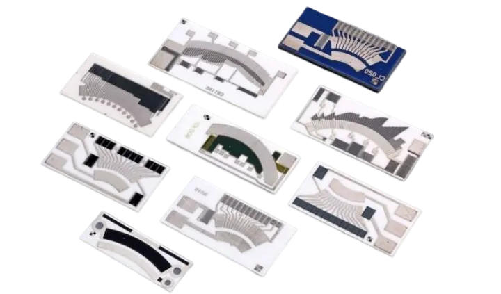
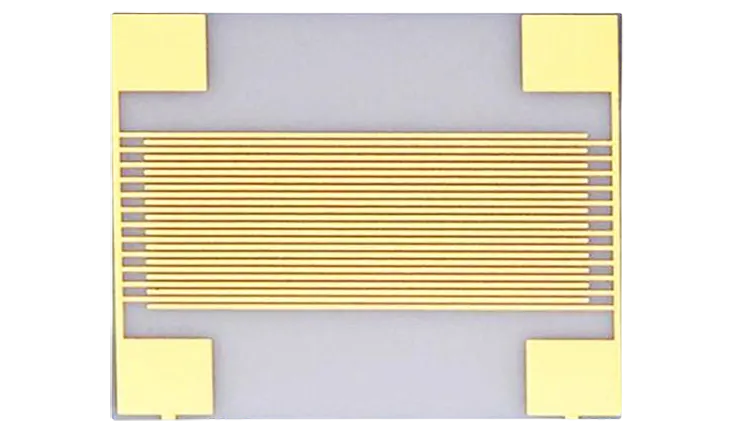
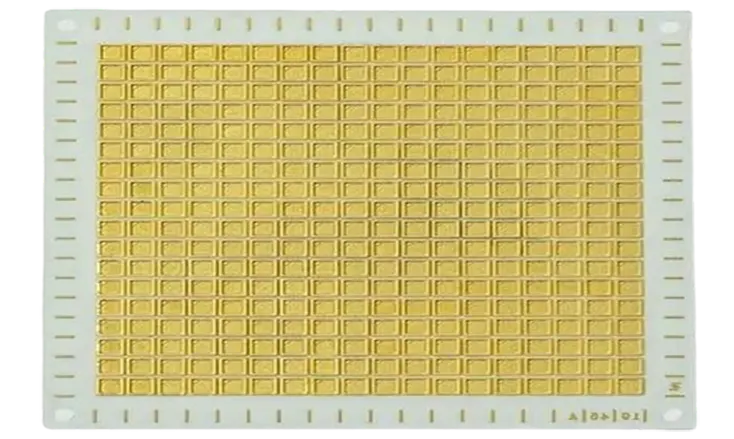
Boron Nitride Ceramic PCB is a kind of printed circuit board that utilize boron nitride ceramic as the base material instead of the usual materials like FR4 or polyimide. Boron nitride ceramic is a material known for its high thermal conductivity, superb electrical insulation and strong mechanical properties. These PCB are gaining popularity, in demanding applications that can effective heat dissipation and dependable operation even in tough conditions.
Advantages in Boron Nitride Ceramic PCB
Boron Nitride ceramics has a high heat capacity, exceptional thermal conductivity, ease of machining, high lubricity, low dielectric constant and high dielectric strength.
JarnisTech is a leading PCB maker in China We provide a wide range of PCB boards. Particularly the Ceramic PCB series. If you are looking for the highest high-end Boron Nitride(BN) PCB, please contact us, and we’ll discuss details for any PCB project.
Boron Nitride Ceramic PCB offer several notable advantage over other types of PCB, as its unique properties. These benefit include:
● High Thermal Conductivity
● High Dielectric Strength
● Low Dielectric Constant
● Excellent Machinability
● Excellent Electrical Insulation
● High Lubricity
● Chemical Stability
● High Temperature Resistance
These benefit make Boron Nitride Ceramic PCB an ideal choice for a broad range of demanding application, including high power and high frequency circuits, communication device, aerospace and automotive.
Applications of Boron Nitride Ceramic PCBs
Boron Nitride Ceramic PCB have become a choice for high performance electronic application as their superior properties compared to traditional PCB material. They are being widely adopted in applications, for their numerous benefit and advantage. Below are an examples of the typical uses of Boron Nitride Ceramic PCB.:
● High-frequency circuits
● Power electronics
● Aerospace and defense
● Computing
● Medical equipment
Applications and Unique Properties of Boron Nitride
Boron Nitride powder, known for its chemical inertness, high dielectric constant, low coefficient of friction and high thermal conductivity, so as a highly versatile material. It finds applications in various fields such as cosmetics, ceramics, oil and gas production, aerospace and electronics.
Due to their unique properties, boron nitride-based ceramics, known for exceptional chemical and thermal stability, rank highly for high temperature equipment components. Additionally, boron nitride is used to create nanotubes in nanotechnology. These BN-based nanotubes, similar in structure to carbon nanotubes, they are formed by rolling BN or graphene sheets into cylindrical shapes. Despite sharing this basic structure, their distinct properties differentiate them.
Comparison of Boron Nitride Ceramics
| Grade | BN-BO | BN-SZ | BN-AlN |
| Compositions | BN>98% | BN+SiC+ZrO2 | BN+AIN |
| Binder | B2O3 | / | AlBO3 |
| Density | 2.1-2.2 g/cm3 | 2.3-3.0 g/cm3 | 2.5-2.6 g/cm3 |
| 25°C Volume Resistivity | >1013 Ω·cm | >1012 Ω·cm | >1014 Ω·cm |
| Max. Service Temp. (°C) Oxygen; Inert Gas; High Vacuum | 900 | 900 | 900 |
| 2000 | 1700 | 2100 | |
| 1800 | 1700 | 1900 | |
| Flexural Strength | 75 Mpa | 100 Mpa | 130 Mpa |
| Compressive Strength | 100 Mpa | 300 Mpa | 250 Mpa |
| Coefficient of Thermal Expansion 25-1000°C | 2.0 *10-6/k | 4.0 x 10⁻⁶/k | 4.5 x 10⁻⁶/k |
| Thermal Conductivity | 30 W/mK | 40 W/mK | 60 W/mK |
Boron Nitride for Thermal Management of Electronic Devices
Boron Nitride, it is stands out as a rare material possessing both thermal insulation and electrical conductivity properties, making it a highly beneficial choice for high power electronic heat spreaders and heat sink application. Aluminum Nitride, beryllium oxide, and occasionally alumina are typical materials used for these application but are generally more challenging to cut into intricate shapes.
W-BN is considered the choice for a dielectric substrate material that can be used in electronic, optical and 2D graphene based devices. When it comes to heat dissipation these materials excel in effectiveness. C-BN is more suitable for purposes whereas H-BN ceramic is the preferred option for crafting C BN crucibles. If you’d like to learn more, about our offerings and how we can tailor them to your needs please reach out to us. Our team is committed to delivering top notch products and services while prioritizing your requirements.
JarnisTech: High-quality Ceramic PCB Manufacturer
JarnisTech is renowned as one of the top ceramic PCB manufacturer and specializes in using 3D-DPC technology for ceramic PCB production. To better serve the requirements of customers, JarnisTech also offer other manufacturing method that cater to their individualized need.
Our company offer a complete range of service for ceramic PCB, such as PCB assembly, as well as other niche product. Including aluminum nitride PCB, alumina PCB, Beryllium Oxide, Silicon Carbide, Boron Nitride and SiC PCB, IGBT modules, COB LED modules, DOB LED modules and other. We are committed to delivering exceptional quality and service and looks forward to discussing how it can assist with your unique manufacturing requirements.
The Capability of Our PCB Manufacturing Facility
We are dedicated to providing top notch PCBs at prices. Rest assured our prototype PCB boards will reach you within 1-2 weeks. There’s no requirement for a minimum order quantity, on our products.
Using sophisticated modern equipment, our team of adept engineers, product experts, and technicians ensure every aspect of your PCB project is perfected. We match our diverse range of customer needs with custom-designed 1-layer, 2-layer, and four-layer Boron Nitride PCB.
We prioritize customer satisfaction, and provide a convenient link to request a customized quote for those customers who wish to modify their PCB choose or make an online purchase. To guarantee an optimal product outcome for your project, our Engineering department will check your PCB Gerber files and collaborate with the appropriate department upon the receipt of your request.
Challenges and Limitations of Boron Nitride Ceramic PCBs
While Boron Nitride Ceramic PCB provide many benefit they also encounter certain challenges and limitations that could impact their use in specific application.
High Cost: Boron Nitride Ceramic compared to traditional PCB material, the cost of manufacturing Boron Nitride Ceramic PCB can be higher as Boron Nitride Ceramic is relatively expensive material.
Limited Availability: Sourcing the material for large scale production can be challenge because the production of Boron Nitride Ceramic powder is not as widespread as other ceramic materials.
Limited Design Flexibility: As the more complex fabrication process for Boron Nitride Ceramic PCB compared to traditional PCB material. Therefore, the design flexibility of the PCB may be limited.
Brittle Material: Boron Nitride Ceramics fragility can lead to decreased durability and shorter product lifespan as its tendency to crack and break when subjected to stress.
Surface Finish Challenge: Applying and maintaining a suitable surface finish for soldering and component attachment can be challenge as Boron Nitride Ceramic’s high surface energy.
Thermal CTE Mismatch: Stress and cracking as CTE mismatch can result from Boron Nitride Ceramic’s low coefficient of thermal expansion (CTE) compared to metals and other materials commonly used in electronic components.
Limited Standardization: Ensuring consistent quality and performance can be challenging as the relatively few industry standard and specifications for Boron Nitride Ceramic PCB compared to other traditional PCB material.
Sum Up
Boron Nitride Ceramic PCB to be used in a range of high performance electronic applications, such as 5G networks, computing, aerospace and defense, due to their properties of high thermal conductivity, excellent electrical insulation and good mechanical strength. As electronic device and components continue to shrink in size and increase in power, the need for such circuit boards type will continue to grow, making the future outlook for Boron Nitride Ceramic PCB promising.
Ongoing research and development effort aim to improve the material properties and manufacturing techniques of Boron Nitride Ceramic PCB, addressing challenge such as cost, limited design flexibility and surface finish issues. Additionally, effort toward industry wide standardization may help to ensure consistent quality and performance of Boron Nitride Ceramic PCB.
At JarnisTech, we sincerely invite you to contact us for further details on our capabilities and how we can assist with your PCB designs. Our Boron Nitride PCB that known for their exceptional quality, have earned us the trust and reliance of our customers. To assist clients with their PCB designs, JarnisTech – a leading PCB maker in China, offers a range of ceramic PCB fabrication service.
Related Posts:
●Overview of Alumina Substrate
●How Layout a Multilayer Ceramic PCB Stack-ups?
●How to Design a Ceramic Circuit Board?
●Leading Global 12 Ceramic PCB Manufacturers
●Manufacturing Standards for Ceramic PCB Production
●What is Ceramic Packages and Its Types?
PCB Fabrication
Ceramic PCB Manufacturing & Assembly


