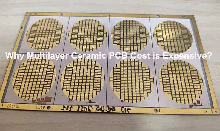
Multilayer ceramic printed circuit boards provide performance at high frequencies, effective thermal management and reliable operation in challenging conditions. Despite their qualities multilayer ceramic PCBs are typically more costly than other types of PCBs. This article aims to explore the reasons, behind the price tags attached to multilayer ceramic PCBs. By uncovering these factors we can better grasp the intricacies of their manufacturing process. Appreciate the distinct benefits they bring to the table.
What is Multilayer Ceramic Circuit Boards?
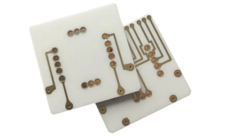
A multilayer ceramic circuit board, commonly referred to as a ceramic PCB or MLCC is a printed circuit board that uses ceramic materials as its base. This type of PCB has feature and benefit tailored to particular uses.
The base of multilayer ceramic PCB usually consists of ceramic material. Include alumina (Al2O3) or aluminum nitride (AlN). These ceramic offer heat conductivity, strong rigidity and stable dimensions. They also exhibit low dielectric loss and excellent high frequency performance, making them suitable for application that require reliable signal transmission at high frequency.
The process of creating a multilayer ceramic PCB involves stacking ceramic substrates together and connecting them using conductive traces, vias and solder joints. These layers are then bonded through high temperature firing to create an reliable structure. Multilayer ceramic PCB find use in applications such as RF and microwave circuits, power amplifiers, high speed digital communication systems and automotive electronics. Their exceptional performance at frequencies, minimal signal loss properties and effective heat dissipation capabilities make them well suited for these purposes. The substrates ability to efficiently dissipate heat is particularly beneficial, in high power settings.
Moreover multilayer ceramic PCBs provide strong protection against environmental elements like moisture, chemicals and temperature changes. This improves their dependability and longevity, in challenging working environments. As a result multilayer ceramic circuit boards stand out as a kind of PCB that utilizes the outstanding characteristics of ceramic materials to deliver top notch high frequency performance, efficient heat control and dependable operation customized for particular uses.
Factors Contributing to High Cost of Multilayer
Ceramic PCBs
Raw Materials and Manufacturing Processes
Multilayer ceramic printed circuit boards utilize high quality alumina (Al2O3) or advanced ceramic substances as bases which’re expensive to extract, process and manufacture due to strict purity standards and the necessity to produce thin flat bases. Copper or other conductive materials are utilized for establishing connections and the intricate patterns and gaps needed in PCBs, with multiple layers raise the copper quantity required, further escalating the expenses. The lamination procedure, which entails bonding layers of ceramic base and conductive materials under intense pressure and heat is intricate and demands specialized equipment thereby contributing to the overall cost.
Design Complexity
Multilayer ceramic circuit boards commonly have a high layers count, each requiring unique design and production methods. As the layer count goes up. The complexity and cost of the circuit board increase. Moreover achieving a circuit density involves creating very fine lines and spaces which demand precise manufacturing techniques and specialized equipment leading to higher costs. The utilization of stackup setups, like blind and buried vias further complicates matters and necessitates extra production steps ultimately raising the overall expenses.
Advanced Features and Technologies
Blind and buried vias allow for connections between different layers without appearing on the surface, enhancing signal integrity and reducing electromagnetic interference, but these features require additional manufacturing steps and increase cost. Multilayer ceramic PCBs are commonly used in high speed applications requiring design considerations and materials to maintain signal quality, which can raise costs. Moreover these PCB can include EMI shielding to safeguard electronic parts from interference but incorporating shielding materials and techniques also adds to the overall expenses.
Testing and Inspection
Multilayer ceramic printed circuit boards (PCBs) undergo non destructive testing (NDT) procedures to ensure their quality and reliability. This involves using methods such as X ray inspection and ultrasonic testing that require tools and trained professionals leading to an increase in overall expenses. In addition to this electrical tests are carried out to confirm the functionality of the PCBs and identify any faults, which necessitates the use of test fixtures and advanced equipment further driving up costs. Moreover mechanical inspections that evaluate dimensions, tolerances and surface quality also require specialized measuring instruments and skilled inspectors adding an additional layer of expenses, to the entire process.
Comparison with Other Multilayer PCB Types
When we look at multilayer ceramic PCB in comparison to other types like multilayer FR4 PCB or multilayer flexible PCB various aspects need to be considered. Such as performance, dependability and specific need for different applications.
Performance
Multilayer ceramic circuit boards are known for their performance at high frequencies thanks to their low dielectric loss and high thermal conductivity. This makes them a top choice for applications requiring signal transmission in high frequency settings. On the hand multilayer FR4 and flexible PCBs may not perform as well due to higher dielectric losses and limitations at higher frequencies. Another advantage of ceramic circuit boards is their effective thermal management capabilities, attributed to the superior thermal conductivity of ceramic materials. This feature makes them a great fit, for high power applications where efficient heat dissipation’s crucial. In contrast multilayer FR4 and flexible PCBs may fall short in terms of thermal management capabilities.
Reliability and Durability
Multilayer ceramic circuit boards are known for their rigidity and stability which helps prevent warping and bending. This feature is important for applications that require reliability. On the hand multilayer FR4 boards offer decent stability while flexible PCBs have lower stability due to their flexibility. Multilayer ceramic boards also show resistance, to extreme temperatures, moisture and chemicals making them well suited for tough environments. In comparison multilayer FR4 and flexible PCBs vary in their ability to withstand environmental conditions.
Design Flexibility
Multilayer ceramic circuit boards are usually rigid and not very flexible in shape making them perfect for applications that need a sturdy board structure. On the hand multilayer FR4 boards offer more flexibility in shape while multilayer flexible boards provide the highest level of flexibility. Furthermore multilayer ceramic boards can handle stackup configurations, such as blind and buried vias giving designers more freedom in their designs. Although multilayer FR4 and flexible boards can also support stackups the manufacturing processes and design considerations, for these materials may vary.
Cost
Multilayer ceramic printed circuit boards tend to be pricier compared to multilayer FR4 PCB and flexible PCB. The increased expense mainly stems from the utilization of quality ceramic substrates and copper conductors, which are costlier raw material. In addtion, the intricate manufacturing processes and specialized equipment required for these PCB significantly contribute to their elevated cost.
Strategies to Reduce Multilayer Ceramic PCB Costs
Cutting down the expenses of ceramic PCB can be accomplished through a range of approaches. Below are a strategie worth exploring.
Optimize Design
Minimize the number of layers in the PCB design to reduce material and manufacturing costs by ensuring that all layers are essential for meeting functionality and performance requirement. Keep things straightforward by avoiding complex elements like blind and buried vias that can drive up manufacturing costs. Also make sure to place components to make routing more efficient which will help minimize the need, for extra vias and layers
Material Selection
Consider alternative ceramic substrate material that offer lower costs while still meeting the necessary specifications. It might be suitable to consider material, with lower thermal conductivity or dielectric properties as long as they meet the application need. Also it’s worth examining the thickness of the copper foil and choosing an option if feasible as this could help lessen material usage and cut down on expenses.
Manufacturing Process Optimization
To reduce costs and enhance efficiency, optimize the panelization of PCBs during manufacturing to maximize material utilization and minimize waste. It’s also beneficial to create PCBs with design guidelines that match up with what the manufacturer can handle which helps avoid production steps or expensive machinery. Introducing automation, into manufacturing operations can also boost efficiency decrease mistakes and bring down labor expenses.
Supplier Selection and Negotiation
In order to save money without sacrificing quality it’s an idea to get price quotes from several PCB manufacturers compare the prices and choose the most economical option. Moreover establishing lasting partnerships, with PCB suppliers can lead to pricing and terms by taking advantage of volume discounts and repeat orders.
Value Engineering
Collaborate closely with PCB manufacturers and design engineers to pinpoint chances for cutting costs without sacrificing quality or dependability. This might entail reworking aspects or parts to simplify and lower expenses. Moreover standardizing components across PCB designs can take advantage of economies of scale, leading to lower procurement costs.
Testing and Quality Assurance
Collaborating with PCB manufacturers to optimize testing processes and reduce testing time without compromising quality is key. Furthermore crafting PCBs with testability, as a priority. Like integrating test points and probes. Can simplify testing protocols. Cut down expenses.
Note:
To effectively cut costs it’s important to take into account how it may affect performance, reliability and any unique need of the applications. Balancing cost reduction with the desired functionality and quality is crucial to ensure the overall effectiveness of the multilayer ceramic PCB.
Final Thoughts
The higher cost of multilayer ceramic PCBs is justified by various factors, such as the expense of raw materials the complexity of the manufacturing process intricate design requirements, advanced features and the extensive testing needed to ensure quality. Despite their price tag these PCBs come with clear benefits. They offer high frequency performance, excellent thermal management and enhanced reliability in challenging environments. Investing in multilayer ceramic PCBs is often necessary to meet specific performance requirements for high end applications. As technology advances and manufacturing processes become more efficient we may see a decrease in costs over time. Nevertheless multilayer ceramic PCBs continue to be a choice, for applications that prioritize exceptional performance and reliability.

