
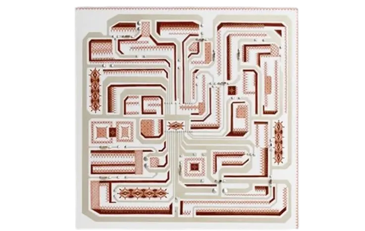
Beryllium Oxide (BeO) ceramic PCB is gaining traction in high performance electronics due to their exceptional properties. Such as outstanding thermal conductivity, high strength, durability and resistance to harsh environment. These advantage over traditional PCB board make it a promising choice for high power and high frequency application.
However, handling Beryllium Oxide ceramic PCB require careful management to ensure safe handling and disposal. This article aims to provide comprehensive insights into the applications, advantages and limitation of BeO ceramic PCB.
What Is Beryllium Oxide?
Beryllium Oxide (BeO), it also known as Beryllia, It is a highly desirable material used in applications where efficient heat dissipation is critical. Its superior thermal conductivity allows BeO to exhibit thermal performance at ambient temperatures that is approximately ten times higher than that of Alumina.
BeO ranks second only to diamond among preferred insulating materials. With a low dielectric constant of 6.76 and a low dielectric loss tangent, BeO enhances circuit performance at higher frequencies. This unique combination of properties makes BeO an ideal material for various electronic application.
Beryllium Oxide has a CTE of 9.0, it is intermediate compared to commonly used electronic material like silicon and gallium arsenide. BeO ceramic PCB demonstrate high thermal stability in harsh operating conditions, making it an excellent choice for high stress electronic applications.
Advantages and Applications of Beryllium Oxide Ceramics
Advantages
BeO ceramic possesses unique and highly desirable physical and dielectric properties that are challenging to replicate in other ceramic. It known for its exceptional strength and excellent specific stiffness characteristics. BeO is one of the strongest ceramic material available. Its low dielectric loss properties make it an ideal material for the electrical industry, complemented by its high electrical resistance performance.
When comparing BeO to other ceramics, it exhibits all the desirable physical and dielectric properties of aluminum oxide. Whats more it has a conductivity that is ten times higher than alumina and 50% greater than aluminum nitride. The dielectric constant of BeO is lower than both aluminum nitride and alumina and its weight per volume is 25% less than alumina and 10% lower than aluminum nitride. BeO proves to be a promising material, for conducting both heat and electricity with performance characteristics that might even outshine those of diamond.
Applications
● Electronic:
BeO ceramic PCB is commonly used for substrates, because of its strong thermal conductivity and impressive electrical resistivity. In addition, since BeO have efficient heat sink performance. It is widely preferred in high power electronics and high speed computer circuits.
BeOs distinct properties and non conductive behavior in the presence of radiation make it a perfect choice for windows and antennas, in microwave communication systems and microwave ovens. This features allows BeO to be utilized in various applications and industries, highlighting its versatility and potential in diverse electrical and electronic settings.
● Medical:
BeO ceramic is widely favored in technology equipment in different industries due to its exceptional thermal conductivity, high dielectric constant and low dielectric loss characteristics. These ceramics can endure elevated temperatures. Effectively disperse heat making them a popular option for a variety of electronic uses such, as portable defibrillators, telecommunications systems, wireless network components and terminations.
In addition BeO is widely employed in life sciences applications, such as gas lasers for DNA and tissue analysis along with field and confocal fluorescence microscopy device. The distinctive electrical properties of BeO make it a perfect choice, for these uses and its outstanding performance enables the equipment to function effectively and precisely.
● Lasers:
BeO’s suitability for use in high temperatures crucibles for industrial melting stems from its chemical and thermal stability. This stability, combined with BeO’s high strength and stiffness, also make it an ideal material for structural elements in mechanical systems. like end-effectors and arm parts. In semiconductor handling equipment, BeO ceramics are an excellent choice for wafer chucks and other components due to their superior electrical performance and unique thermal management propertie.
Enabling commercial systems to function efficiently and reliably, BeO finds use in high end laser diodes. Its excellent thermal conductivity and low dielectric loss characteristics make BeO an ideal material for use in high powered industrial lasers for cutting and marking. Furthermore, its exceptional optical propertie make BeO ceramics ideal for applications in long range optical fiber transmission.
● Energy:
Moreover BeO ceramics exhibit electrical and thermal durability enabling them to operate effectively as power amplifiers and controllers in various industrial settings. Widely employed in the oil and gas sector for drilling purposes BeO ceramics provide strength and resistance to high temperatures. The distinctive characteristics of BeO render it a preferred material for utilization, in applications leveraging its superior thermal conductivity and minimal coefficient of thermal expansion to optimize device functionality.
Furthermore the distinctive in situ X ray analysis characteristics of BeO are valuable in the field of drilling aiding in the interpretation of data from deep within the earth. Additionally BeO ceramics prove to be well suited for application, in concentrating photovoltaic (CPV) systems enhancing the efficiency of cells through their excellent thermal conductivity and minimal dielectric constant.
Its exceptional performance properties ensure reliable and efficient performance across a wide range of industries, including application such as switches, modulators, receivers, and transmitters where BeO ceramics find use.
● Military And Aerospace:
The strong and rigid nature of the material makes it perfect for modules that need to withstand tough conditions last long and resist high temperature. BeO ceramics have thermal conductivity and great electrical insulation, it’s that make BeO suitable for high frequency electronic modules.
Moreover BeO is widely favored for its electrical insulation characteristics especially in modules that demand superior electrical isolation like guidance modules. Its distinct dielectric properties and minimal dielectric loss coefficient also contribute to its effectiveness in microwave and millimeter wave communication modules guaranteeing data transmission with minimal disruption from noise.
Across a diverse array of application and electronic modules, BeO ceramic is distinguished for its exceptional electronic performance. This includes radar modules where high precision is crucial, enhanced by the material’s excellent thermal stability.
● Wireless Communications:
BeO ceramics possess exceptional thermal conductivity, high electrical resistivity, and low dielectric loss coefficient, making it ideal for high frequency communication applications. Making BeO ceramics a critical component of satellites’ communication modules, the material’s thermal management performance ensures electronic modules operate efficiently in high temperature environment.
Guaranteeing consistent data transfers with minimal interference and signal quality degradation, the low dielectric loss coefficients of BeO, combined with its high thermal conductivity, ensure optimum performance of electronic devices by minimizing heat related issues. These high strength characteristics and unique dielectric properties make BeO an ideal material for point-to-point and point-to-multipoint radios.
Crucial factors like high reliability, durability, and high temperature stability make BeO ceramic a popular choice in specialized application. And its outstanding electronic performance further enhances make it is very suitability for these demanding uses.
Limitations of Beryllium Oxide Ceramic PCB
Limitations of Beryllium Oxide Ceramic PCB include:
●High Cost
●Brittle performance
●Hazardous materials
●limited availability in the market
Comparison of Beryllium Oxide Ceramic PCB to Traditional PCB
Beryllium Oxide Ceramic PCB offer several advantages over traditional PCB like FR4 and Aluminum based PCB.
● High Thermal conductivity
● High strength and durability
● High dimensional stability
● Low dielectric loss
● Resistance to chemical and corrosive materials
Beryllium Oxide Ceramic vs Alumina Oxide and Aluminum Nitride
In the presence of chemical oxidizers, BeO ceramics exhibit unique chemical stability, surpassing AlN ceramics. With a thermal conductivity that can reach 325 W/(m*K), approximately 50 percent higher than aluminum nitride (AlN), BeO ceramics offer nearly ten times greater efficiency compared to aluminum oxide (Al2O3) ceramics.
Resistant to high temperatures, BeO ceramics perform effectively in application where liquid cooling or airflow is impractical. Their exceptional quality make them an ideal choice for application requiring both electrical insulation and high thermal conductivity. Ranked second only to diamonds in thermal conductivity among electrically insulating material, BeO ceramics stand out for their impressive performance.
BeO ceramics are well suited for use in crucibles meant for melting metals at high temperature. They stand out as a choice for their resistance to both heat and chemicals. Industries can benefit from the nature and electrical insulation properties of BeO ceramics enabling them to shrink the size of enclosures. The careful design of these ceramics play a role in ensuring optimal product performance making them a perfect fit that for various application.
Beryllium Oxide Ceramic Substrates Description
Beryllium oxide, it also known as beryllia, is renowned for its exceptional electrical insulation properties, comparable to alumina, placing it among the top electrical insulators. Furthermore, its superior thermal conductivity rivals even the most conductive metals, establishing it as a leading ceramic in its class. These high performance ceramics are crafted from high purity beryllium oxide based materials, resulting in the production of beryllium oxide ceramic substrates.
BeO substrates has boast a flawless surface finish that enhances compatibility with metal components, they are crafted to meet precise dimensional tolerances through precision focused fabrication techniques. Achieving full densification, these components are produced via ceramic fabrication methods and are sintered at temperatures exceeding 1500 degrees Celsius.
BeO ceramic substrate is often the choice for various electronic uses because of their excellent electrical insulation. BeO ceramic substrate also support performance stability in high heat areas by reducing thermal stress through efficient heat dissipation. This thermal conductivity property, combined with their unique thermal mechanical and dielectric performance, they make that BeO substrate ideal for electronic application.
Beryllium Oxide Ceramic Substrates Specifications
| Testing Entries | Testing Conditions | Properties |
| Flexural Strength | / | ≥170MPa |
| Thermal Conductivity | 25℃ | ≥250W/m·k |
| 100℃ | ≥190W/m·k | |
| Permittivity | 1MHz 20℃ | 6.5-7.5 |
| 10GHz 20℃ | 6.5-7.5 | |
| Volume Resistivity | 25℃ | ≥10^14Ω·cm |
| 300℃ | ≥10^11Ω·cm |
Why Wouldn’t You Make Use of BeO as the Basis for Making DBC Ceramic PCB
BeO is an exceptional material for ceramic PCB, It provide superior thermal conductivity of 200-250 W/m·K, a high dielectric constant of 6-7 at 0.1 MHz, and low dielectric loss tangents of 10⁻⁴ at 0.1 GHz, even under extreme temperature conditions. However, BeO is less commonly used as a ceramic substrate material compared to popular alternatives like Al₂O₃, Si₃N₄, AlN, or ZrO₂, primarily due to the extreme toxicity of BeO powder.
BeO is typically produced through the reaction of beryllium with oxygen at temperatures ranging from 1065 -1085 degrees Celsius. The production process is mainly limited to the use of cobalt on BeO substrate, which has driven the increased demand for Aluminum Nitride as an alternative substrate material. Currently, only a few countries, including the USA, Russia and China, manufacture ceramic PCB using BeO. While the USA has been advanced in producing BeO, some companies in China produce BeO raw materials, and only a few firms manufacture direct copper bonded (DCB) on BeO due to environmental restriction.
BeO is not commonly used in DBC technology due to toxicity concerns. However, it is suitable for thick film technologies where metallization of the ceramic PCB conductor. Like Au or AgPd, is applied to the BeO substrate via silkscreen printing. The drying temperature is approximately 850°C, eliminating the need for high temperature environment, which minimize chemical reactions and reduces environmental concerns.
Safety Concerns and Handling Precautions of BeO PCB
Handling beryllium oxide ceramic comes with safety consideration and necessary precaution cos its potentially harmful characteristics.
Inhalation hazard:
Inhaling dust and particles, from beryllium oxide ceramics can be harmful. It may lead to lung damage or beryllium disease an untreatable lung illness.
Skin and eye irritation:
When contact with beryllium oxide ceramic maybe cause skin and eye irritation resulting in redness, itching and inflammation.
Environmental hazard:
Beryllium oxide ceramic is classified as hazardous waste therefore manufacturer must dispose of it correctly to prevent harm to the environment.
To mitigate these safety concern, when dealing with BeO ceramic PCB it is important to follow safety measure to address these concern.
● Use personal protective equipment (PPE): Remember to put on protective gear (PPE). like gloves, protective clothing and eye protection when working with BeO PCB. This is important to avoid skin and eye irritation well as inhalation exposure.
● Use engineering controls: Engineering controls, inclued local exhaust ventilation, should be in place to prevent inhalation exposure to beryllium oxide ceramic dust and particles.
● Proper disposal: BeO PCB waste must be disposed of following both local and federal guideline to prevent environmental contamination.
● Training: Employees must undergo training on how to handle, use and dispose of beryllium oxide PCB to reduce the chances of workplace exposure and guarantee adherence, to safety protocols.
Final Thought
Talk To Our Technical Ceramic PCB Experts
Beryllium Oxide Ceramic PCB has a lot going for it compared to regular PCB. It’s got high thermal conductivity, great strength and durability, excellent dimensional stability, low dielectric loss, and it can handle chemicals and corrosion pretty well. But, it’s not all perfect, it’s more expensive, quite brittle, and has some hazardous properties.
Future developments and research directions for Beryllium Oxide Ceramic PCB can include better thermal management, boosting mechanical strength, cutting cost, integrating with advanced tech and ramping up production. Beryllium Oxide Ceramic PCB is a promising material for high performance electronics, particularly in applications where thermal management and reliability are critical requirement.
At JarnisTech, with our unique blend of materials that are formed, fired and fabrication techniques, we are able to provide our customers with the finest quality Beryllia ceramic PCB boards. Therefore, Our comprehensive range of BeO ceramic PCB is available for procurement, offering both dry pressing and iso pressing methods to accommodate the specific design requirements of your PCB project.
For information on our top notch BeO ceramic PCB board and its advantages for your PCB project feel free to reach out to us via email at [email protected] or by calling 0086 755 23034656. As professionals in the industry we are committed, to delivering customer service and assistance.
Related Posts:
●Overview of Alumina Substrate
●How Layout a Multilayer Ceramic PCB Stack-ups?
●How to Design a Ceramic Circuit Board?
●Leading Global 12 Ceramic PCB Manufacturers
●Manufacturing Standards for Ceramic PCB Production
●What is Ceramic Packages and Its Types?
PCB Fabrication
Ceramic PCB Manufacturing & Assembly


