
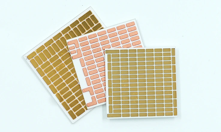
Ceramic PCB manufacturing involves a methodical approach to ensure high standards throughout each production phase. From choosing the right materials to employing advanced fabrication techniques, the process demands careful consideration at every step. This includes material preparation, metallization, high-temperature firing, and finishing processes, all of which contribute to creating a durable and reliable end product. By optimizing these processes, we can achieve the precision required for applications in sectors such as telecommunications, medical devices, and industrial systems, ensuring their ceramic PCBs are capable of performing under demanding conditions.
Introduction to Ceramic PCB Production and Manufacturing Standards
In modern electronics applications, Ceramic PCB Production has emerged as a reliable solution for applications requiring robust thermal management and mechanical stability. Ceramic PCB Manufacturing processes have evolved to meet the stringent demands of industries such as aerospace, automotive, medical devices, and telecommunications. Adhering to established manufacturing standards ensures consistency, reliability, and performance in Ceramic PCB Fabrication. This section delves into the nuances of Ceramic PCB Manufacture, exploring its applications, process evolution, and the significance of adhering to manufacturing standards.
Understanding Ceramic PCB Production in High-Tech Industries
Ceramic PCB Production is integral to high-tech industries where devices are subjected to extreme conditions. For instance, in aerospace applications, Ceramic PCBs are utilized for their ability to withstand high temperatures and mechanical stress. Similarly, in medical devices, the biocompatibility and reliability of Ceramic PCB Manufacturing processes ensure patient safety and device efficacy. The following table illustrates the application of Ceramic PCBs across various industries:
| Industry | Application Example | Requirement Addressed |
| Aerospace | Satellite communication modules | High thermal stability |
| Automotive | Engine control units | Vibration resistance |
| Medical Devices | Implantable sensors | Biocompatibility |
| Telecommunications | High-frequency signal transmission | Low dielectric loss |
By embracing Ceramic PCB Fabrication, these industries achieve enhanced performance and reliability in their electronic components.
Evolution of Ceramic PCB Manufacturing Processes
The journey of Ceramic PCB Manufacturing has seen significant advancements. Initially, the process involved basic techniques with limited material options. Over time, innovations have introduced materials like aluminum nitride and beryllium oxide, offering superior thermal conductivity and mechanical strength. Modern Ceramic PCB Fabrication techniques include:
●Thick Film Technology: Involves screen printing conductive pastes onto ceramic substrates, suitable for high-power applications.
●Thin Film Technology: Utilizes vacuum deposition methods for precise circuit patterns, good for high-frequency applications.
●Direct Bonded Copper (DBC): Bonds copper directly onto ceramic substrates, enhancing thermal performance.
●Active Metal Brazed (AMB): Employs active metal alloys to bond copper to ceramics, offering strong adhesion and thermal conductivity.
These advancements in Ceramic PCB Manufacture have expanded the scope of applications, enabling the development of compact, high-performance electronic devices.
The Importance of Standards in Ceramic PCB Fabrication
Adherence to manufacturing standards in Ceramic PCB Fabrication is must for ensuring product quality and reliability. Standards such as IPC-6012 and ISO 9001 provide guidelines for material selection, process control, and quality assurance. Compliance with these standards ensures that Ceramic PCB Manufacturing processes meet industry requirements and customer expectations.
For example, IPC-6012 outlines performance and qualification requirements for rigid PCBs, including those made from ceramic materials. ISO 9001 focuses on quality management systems, ensuring consistent product quality and continuous improvement in Ceramic PCB Production.
By aligning with these standards, PCB manufacturers can deliver Ceramic PCBs that meet the rigorous demands of various industries, fostering trust and long-term partnerships with clients.
Core Materials for Ceramic PCB Manufacturing and Fabrication
In ceramic PCB production, material selection forms the base of the entire process flow. Every substrate brings its own performance profile to the table—shaping everything from thermal conductivity and mechanical stability to processing compatibility. This section explores common ceramic materials and how us align them with real-world product requirements across applications like RF devices, laser systems, and power converters.
Properties of Alumina, Aluminum Nitride, and Beryllium Oxide
Ceramic PCBs are built on substrates chosen for their ability to handle stress—both thermal and electrical. Here’s a breakdown of what each material brings to the production line:
Alumina (Al₂O₃)-
●Offers stable performance for general-use PCB fabrication
●Common in cost-sensitive applications with moderate thermal demands
●Compatible with both HTCC and LTCC processes
Aluminum Nitride (AlN)-
●Provides higher thermal conductivity than Alumina
●Well-suited for LED modules, RF power amplifiers, and base station units
●Often used in multi-layer ceramic PCB production where thermal flow matters
Beryllium Oxide (BeO)-
●Delivers extremely high heat dissipation capability
●Applied in aerospace-grade systems and industrial-grade frequency control modules
●Requires controlled manufacturing due to material handling safety measures
Choosing between these materials involves more than performance metrics—it’s about long-term reliability under specific load cycles.
Material Selection Criteria for Ceramic PCB Manufacture
When defining a ceramic PCB layout, every decision about the base substrate is rooted in actual system needs. We must to evaluate materials based on how well they work within the final assembly—not just on spec sheets.
Thermal Conductivity-
●Determines how effectively heat moves through the board and away from power-intensive components.
Electrical Insulation-
●Keeps circuits electrically isolated to reduce cross-talk and signal interference.
Mechanical Strength-
●Prevents substrate cracking or delamination under vibration or repeated temperature shifts.
CTE Compatibility (Coefficient of Thermal Expansion)-
●Minimizes the risk of solder joint fatigue or pad lifting when paired with mounted components.
Therefore, if you’re designing for RF comms or multi-channel power conversion, the board needs to match the workload. Think practically—match function to form.
LTCC vs HTCC Technologies in Ceramic PCB Production
LTCC and HTCC processes serve different fabrication needs. While both allow multi-layer structures, the way they’re built impacts cost, durability, and use-case suitability.
LTCC (Low Temperature Co-fired Ceramic)-
●Fired at ~850°C, compatible with silver or gold metallization
●Enables compact, multilayer circuits with better signal routing
●Common in mobile, GPS, and precision RF components
HTCC (High Temperature Co-fired Ceramic)-
●Fired at ~1600°C using tungsten or molybdenum as conductors
●Offers robust mechanical strength for demanding environments
●Used in defense electronics, laser drivers, and industrial-grade converters
Choosing Between Them-
●LTCC suits compact modules where layout density and signal handling matter
●HTCC favors heat-dense applications with a focus on board resilience
The fabrication method isn’t just a technical checkbox—it’s part of the long game in product reliability.
Detailed Manufacturing Process of Ceramic PCBs
The production of ceramic PCBs involves multiple tightly controlled processes that transform raw ceramic substrates into high-performance circuit boards used across telecommunications, high-current power modules, medical devices, and advanced industrial systems. This section outlines the main stages of ceramic PCB manufacturing, with a focus on precision and repeatability required for high-density and high-temperature applications.
Substrate Formation and Preparation
The journey begins with substrate development, which lays the foundation for subsequent metallization and patterning.
●Material selection: Common ceramic materials include alumina (Al₂O₃), aluminum nitride (AlN), and beryllium oxide (BeO), selected based on thermal conductivity, dielectric strength, and mechanical properties.
●Tape casting (for LTCC): A slurry of ceramic powder and binder is cast into thin layers for subsequent stacking.
●Green sheet punching (for via creation): Holes for vertical interconnections are mechanically or laser drilled while the ceramic is still in the flexible green state.
●Drying and surface smoothing: Ensures dimensional consistency and surface readiness for metallization.
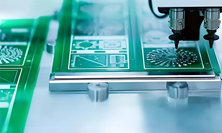
Metallization Techniques for Ceramic Circuits
Metallization enables electrical interconnects on ceramic substrates. The method chosen depends on performance, application, and design layout.
Screen Printing Conductive Pastes-
This technique is used in both HTCC and LTCC processes to form circuit traces:
●Silver, gold, or copper pastes are commonly used based on thermal and electrical demands.
●Mesh type and stencil tension affect line resolution and paste uniformity.
●Post-print drying ensures solvent removal without disturbing the pattern.
Sputtering and Electroplating Processes-
For more precise or multilayer ceramic PCB designs:
●Sputtering deposits a thin seed layer of metal across the substrate, typically titanium-copper or chromium-copper systems.
●Electroplating then thickens these traces, allowing for higher current-carrying capabilities.
●Adhesion testing ensures the metal layer is bonded effectively to the ceramic base.
High-Temperature Firing and Sintering Procedures
Firing turns ceramic substrates and conductive pastes into dense, functional layers:
●HTCC sintering occurs around 1600°C, co-firing both ceramic and metal simultaneously.
●LTCC sintering is typically done at 850–900°C in a controlled atmosphere to prevent oxidation.
●Temperature profile control affects shrinkage rates, mechanical stability, and dielectric integrity.
Via Drilling, Filling, and Metallization
Layer-to-layer interconnections are required for multilayer circuits:
●Laser drilling is used for precise microvias, especially in LTCC.
●Via fill pastes—either conductive or resistive—are applied before lamination.
●Post-firing conductivity tests verify via performance.
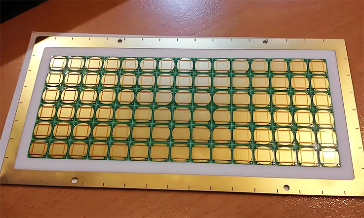
Multilayer Ceramic PCB Lamination
When designs require stacking multiple ceramic layers:
●Layer alignment systems ensure via and trace accuracy across layers.
●Lamination pressure and temperature are controlled to reduce warpage and delamination.
●Embedded passives can be incorporated during lamination for compactness.
Firing, Sintering, and Surface Finishing in Ceramic PCB Manufacture
After lamination, another round of sintering and surface refinement is performed:
●Debinding steps remove organic binders from green tapes.
●Final sintering solidifies both ceramic and internal metallization.
●Surface finish options such as ENIG (Electroless Nickel Immersion Gold), silver plating, or OSP are applied depending on assembly needs.
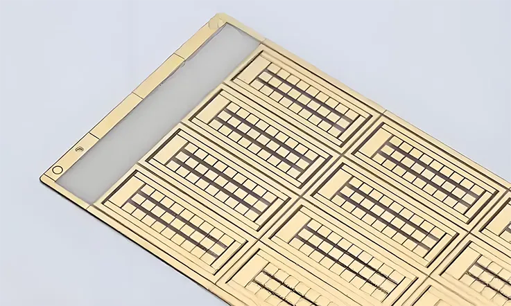
Dicing, Routing, and Final Board Shaping
Boards are cut to final dimensions and edge-finished to meet design tolerances:
●Diamond saw dicing or laser routing ensures clean cuts on brittle ceramic substrates.
●CNC routing is used for complex contours and slot features.
●Post-machining inspection checks for microcracks, chipping, and edge quality.
Manufacturing Standards and Quality Control in Ceramic PCB Production
As ceramic PCB production becomes a staple in high-demand applications like telecommunications infrastructure, medical diagnostic tools, and high-power electronics, manufacturing standards and quality control procedures have evolved into structured systems to enhance consistency and production yield. These systems are framed not only by global certification bodies but also by in-house protocols that address the unique behaviors of ceramic substrates during metallization, thermal cycling, and sintering. Below, we explore how standardized control mechanisms support ceramic PCB manufacturing and fabrication at each quality checkpoint.
ISO Certifications and Industrial Requirements for Ceramic PCB Manufacturing
Compliance with international and industry-specific standards helps maintain process consistency and meet customer specifications for ceramic PCBs, particularly those used in high-frequency, high-voltage, and thermal-sensitive applications.
●ISO 9001: Ensures a structured approach to quality management, emphasizing traceability from raw ceramic substrate to the final plated board.
●ISO 14001: Encourages environmental monitoring during the firing and metallization stages, especially when handling materials like beryllium oxide.
●IATF 16949: Applied for clients in automotive electronics, covering the full ceramic PCB production chain, from substrate punching to surface finishing.
●RoHS & REACH compliance: These regulations demand that raw ceramic boards and metallization pastes exclude hazardous substances, which is especially relevant in medical and consumer electronics sectors.
●UL Certification: Indicates the substrate’s flame resistance and dielectric strength, supporting use cases where thermal and electrical stability must meet predefined parameters.
Thermal Cycling, Electrical Testing, and Inspection Methods
Ceramic PCBs undergo comprehensive in-line and post-process inspections designed to validate performance under operating conditions where thermal dissipation, current flow, and physical durability must stay within tolerances.
●Thermal Cycling Tests: Subjecting boards to temperature swings from -55°C to +150°C helps verify the integrity of via fill, metallization adhesion, and substrate bonding.
●Electrical Continuity and Dielectric Testing: HV insulation resistance and continuity tests detect microcracks in multilayer ceramic PCBs.
●Automated Optical Inspection (AOI): Identifies metallization width, spacing defects, and paste spreading issues after screen printing and firing.
●X-Ray Inspection: Applied to detect voids in vias or solder joints, particularly in multilayer or high-density interconnect configurations.
●Surface Profilometry: Used to assess the uniformity of the conductive traces, especially post-sputtering or plating.
Reliability Testing Protocols for Ceramic PCB Fabrication
Long-term durability in actual operating environments is validated through standardized reliability tests. These tests simulate stresses that high-current or high-frequency ceramic PCBs may experience in the field.
●HAST (Highly Accelerated Stress Testing): Accelerated aging using high humidity and temperature conditions to evaluate resistance to delamination.
●Thermal Shock Testing: Rapid transfer between hot and cold environments identifies potential expansion mismatches between metal layers and ceramic substrates.
●Mechanical Shock and Vibration Testing: Applied to detect weaknesses in the lamination or substrate cohesion, typically required by aerospace or defense clients.
●Peel Strength Measurement: Determines the bonding strength between the conductive layer and ceramic substrate, especially in boards that use thick copper.
●Moisture Resistance Testing: Evaluates absorption rates and any conductive leakage paths that may form under prolonged exposure to moisture.
Design Guidelines for High-Performance Ceramic PCB Fabrication
The fabrication of ceramic PCBs used in industrial, high-power, and precision electronic applications requires an engineered balance of thermal, electrical, and mechanical properties. Ceramic PCB fabrication must consider thermal load, electrical behavior, and substrate resilience to meet design specifications across demanding environments such as power electronics, medical devices, telecommunications infrastructure, and aerospace systems. Each factor must be assessed during the early stages of Ceramic PCB manufacturing to align with application-specific functionality.
Thermal Management Strategies for Ceramic PCB Manufacture
Effective heat handling is a fundamental consideration in Ceramic PCB production, particularly in high-current and high-temperature scenarios.
●Use of High-Thermal Conductivity Substrates: Materials such as aluminum nitride (AlN) and beryllium oxide (BeO) offer thermal conductivity values that support the dissipation of large heat loads.
●Substrate Thickness Optimization: Thinner substrates allow faster heat transfer, whereas thicker substrates offer mechanical strength and insulation. The tradeoff should be evaluated based on thermal load profiles.
●Surface Metallization Layer Design: Thick copper plating on ceramic boards improves thermal conduction and current-carrying capability.
Table 1: Thermal Properties of Ceramic Substrates
| Material | Thermal Conductivity (W/m·K) | Typical Thickness (mm) | Recommended Applications |
| Alumina (Al₂O₃) | 24 | 0.25–1.0 | General electronics |
| Aluminum Nitride (AlN) | 170–230 | 0.38–1.0 | High-power, LED, RF applications |
| Beryllium Oxide (BeO) | 250–300 | 0.5–1.5 | Aerospace, RF heating systems |
Ceramic PCBs used in power amplifiers or LED arrays must dissipate heat to prevent degradation of active components. AlN-based substrates with thermal conductivity exceeding 170 W/m·K are common in such designs.
Electrical Performance Optimization in Ceramic PCB Production
Electrical performance requirements vary depending on the operating voltage, frequency, and signal stability demands. Design choices in ceramic PCB manufacture influence these outcomes.
●Dielectric Constant Matching: Proper selection of ceramics with a stable dielectric constant (e.g., 9.8 for alumina) supports impedance control and consistent high-frequency performance.
●High Breakdown Voltage: Materials like Al₂O₃ and AlN offer breakdown voltages over 10 kV/mm, supporting high-voltage circuit insulation.
●Minimizing Parasitic Capacitance: Microstrip or stripline layout techniques can be used with ceramic substrates to reduce EMI and ensure signal integrity in RF modules.
Table 2: Electrical Characteristics of Common Ceramic Substrates
| Material | Dielectric Constant (εr) | Breakdown Voltage (kV/mm) | Application Context |
| Alumina (Al₂O₃) | 9.8 | >13 | Analog circuits, power control |
| Aluminum Nitride (AlN) | 8.5–9.0 | >15 | RF, high-frequency modules |
| Beryllium Oxide (BeO) | 6.5–7.5 | >17 | High-speed, RF heating circuits |
Devices in radar systems or medical imaging benefit from ceramic PCBs manufactured with consistent dielectric layers and minimal variance in line geometry.
Mechanical Integrity and Layout Best Practices
Mechanical stability in ceramic PCB fabrication ensures structural performance under thermal cycling, vibration, or external mechanical stress.
●Coefficient of Thermal Expansion (CTE) Matching: Ensuring CTE compatibility between the ceramic base and mounted components reduces the risk of delamination or microcracking.
●Via Fill and Metallization Control: Proper via metallization using tungsten or copper supports mechanical durability and electrical reliability in multilayer structures.
●Design for Manufacturing (DFM) Alignment: Features such as rounded corners, uniform copper distribution, and precise scribe lines help reduce stress concentrations during dicing and assembly.
Table 3: Mechanical and Layout Considerations in Ceramic PCB Fabrication
| Design Factor | Recommended Range or Practice | Benefit |
| CTE (AlN) | ~4.5–5.0 ppm/°C | Matches well with silicon chips |
| Via Metallization | Copper or tungsten, ≥20 μm thickness | Enhanced conductivity and strength |
| Scribe Line Width | 0.2–0.3 mm | Reduces microcrack propagation |
| Copper Balance | Symmetric copper layout across layers | Minimizes warpage during lamination |
For instance, a telecom filter operating across -40°C to +125°C may use multilayer AlN ceramic PCBs with laser-drilled filled vias to maintain mechanical stability and electrical continuity.
Heavy Copper Integration into Ceramic PCB Manufacturing
The integration of heavy copper into ceramic PCB structures is increasingly adopted in applications where elevated current flow, thermal stress resistance, and mechanical stability are expected. Ceramic materials such as alumina (Al₂O₃) and aluminum nitride (AlN) provide robust electrical insulation and thermal conductivity. When paired with thick copper circuitry, these substrates offer tailored solutions for high-current and high-temperature electronics used in power modules, industrial converters, and automotive control systems.
By combining metallization technologies and layered ceramic engineering, manufacturers can construct circuits that accommodate extreme environments and current densities exceeding 20 A/mm². This section outlines the technical pathways for combining heavy copper and ceramic substrates, along with design considerations and application-specific examples.
Combining Ceramic PCB Fabrication with Heavy Copper Technologies
The process of embedding heavy copper into ceramic substrates requires precise control of metallization and firing techniques. The use of either direct bonded copper (DBC) or active metal brazing (AMB) forms the structural basis of these hybrid assemblies.
●DBC processes utilize a high-temperature eutectic reaction between copper and a ceramic oxide layer, forming a robust metallurgical bond without the need for intermediate adhesives.
●AMB technologies involve reactive metal layers (e.g., titanium) between copper and ceramic, brazed in a vacuum furnace to achieve controlled adhesion with minimal voiding.
●The resulting copper layers can range from 100 µm to over 500 µm in thickness, supporting higher thermal and electrical loads than traditional PCBs.
●Fabrication techniques must address the coefficient of thermal expansion (CTE) mismatch between copper and ceramics to prevent delamination during thermal cycling.
●Conductor etching and routing are optimized using high-speed laser systems or chemical milling processes for precise feature definition.
High-Current Handling Design for Ceramic PCB Manufacture
Heavy copper ceramic PCBs are designed to handle current-intensive applications through careful thermal and mechanical engineering. Conductive trace layout, via structures, and heat dissipation features are all tailored to support stable electrical operation.
●Multi-layer copper stacking with isolated dielectric layers allows parallel current paths and distributed heating zones.
●Thermal vias and copper-filled through-holes provide enhanced vertical heat transfer in multilayer designs.
●Power distribution networks on these boards often utilize planar bus structures for even current dispersion.
●The high melting point and stability of AlN substrates offer reduced thermal resistance compared to organic laminates.
●Accurate simulation of Joule heating and thermal gradients helps avoid hot spots and mechanical fatigue in high-power environments.
Case Studies in Industrial Equipment Applications
In now-world settings, heavy copper ceramic PCBs are deployed in mission-specific applications where consistent current flow and long operational lifespans are required. Several use cases illustrate the benefits of this integration:
●High-Power LED Modules: Combining AlN substrates with 300 µm thick copper enables stable light output and heat removal in continuous-duty lighting for manufacturing plants.
●EV Battery Management Systems: Ceramic PCBs with integrated 500 µm copper conductors are used for safe current routing, reducing thermal stress in confined automotive enclosures.
●Industrial Motor Drives: Multi-layer DBC substrates provide high thermal conductivity paths and strong dielectric insulation, enhancing drive controller reliability in motor operation environments.
●HVDC Power Converters: Heavy copper traces support regulated high-voltage power switching, improving long-term dielectric endurance and efficiency under elevated temperatures.
Advanced Ceramic PCB Manufacturing Techniques for Medical and Communication Sectors
In the domains of medical diagnostics and advanced telecommunications, ceramic PCBs must meet rigorous structural and functional benchmarks. The manufacturing approach must support high-frequency signal transmission, precise component integration, and strict tolerance control. With the integration of advanced ceramic substrates and controlled metallization methods, we can deliver application-specific boards that align with industry-required functionality. The following sections explore the primary focus areas for such production.
Biocompatible Ceramic PCB Fabrication for Medical Devices
Ceramic PCBs for medical applications must meet sterilization requirements, support cleanroom assembly, and withstand repetitive electrical cycling. Biocompatibility is determined by both substrate selection and surface finishing techniques.
●Alumina (Al₂O₃) and zirconia-based substrates are widely used due to their stable surface chemistry and resistance to body fluids.
●Metallization typically utilizes gold or platinum thick-film pastes to ensure corrosion resistance and compatibility with bio-implantation procedures.
●Low-temperature cofired ceramic (LTCC) structures are better when flexible layer stacking is required within implantable sensor modules.
●Production lines must include plasma cleaning stages to eliminate surface contaminants prior to final bonding or encapsulation.
Example: Pacemaker control modules and neurostimulator devices rely on ceramic boards that maintain performance without degradation under bodily exposure or cleaning protocols.
High-Frequency Ceramic PCB Production for 5G and RF Applications
Ceramic substrates are well-suited to support high-frequency data handling, particularly in millimeter-wave and microwave applications such as base stations and radar arrays.
●Aluminum nitride (AlN) substrates are selected for their low dielectric loss and high thermal conductivity, balancing electrical performance with heat dissipation.
●Metallization via sputtering or electroplating ensures fine line resolution needed for high-speed signal routing.
●Laser-drilled vias enable accurate signal transition between layers without affecting substrate integrity.
●Thin-film processing enables integration of impedance-controlled microstrip and stripline geometries.
Example: In 5G antenna modules, ceramic PCBs help maintain signal consistency by supporting minimal reflection and loss, even at frequencies exceeding 30 GHz.
Precision Tolerances and Microstructure Control in Manufacturing
Achieving consistent quality across ceramic circuit production involves dimensional accuracy, substrate flatness, and uniform microstructure distribution.
●Tape casting and lamination steps must be monitored for uniform thickness and pore-free layering.
●Co-firing temperature profiles are optimized to control grain boundary formation and minimize internal stresses.
●Dimensional tolerances are maintained through CNC-based dicing and laser routing, typically achieving accuracy below ±0.05 mm.
●Metallographic inspection ensures conductor adhesion and detects issues such as delamination or cracking.
Example: Diagnostic ultrasound probes require high-density interconnect (HDI) ceramic PCBs with controlled layer registration and precise spacing between transducer channels.
Applications of Ceramic PCB Manufacture in Industrial and High-Power Electronics
Ceramic PCB technology has developed to meet the increasing structural and thermal demands of industrial and high-power electronics. The integration of substrates such as alumina (Al₂O₃), aluminum nitride (AlN), and beryllium oxide (BeO) into robust metallization processes enables ceramic PCBs to support elevated current loads, frequent thermal cycling, and mechanically demanding environments. This section explores selected industrial applications where ceramic substrates are utilized in high-performance electrical assemblies.
Power Modules and Inverter Systems Utilizing Ceramic PCB Fabrication
Ceramic PCBs are utilized in power conversion systems due to their ability to maintain electrical insulation while conducting significant heat away from high-current components.
●Substrates like AlN and BeO offer thermal conductivities exceeding 170 W/m·K, suitable for high-power IGBT and MOSFET modules.
●Direct Bonded Copper (DBC) and Active Metal Brazing (AMB) methods are adopted to achieve thick copper metallization for current handling above 100 A.
●Double-sided and multilayer ceramic PCBs are configured for automotive inverters, energy storage systems, and rail traction modules.
●Manufacturing tolerances are controlled to within ±0.1 mm for alignment with heat sinks and power packaging bases.
LED Modules and High-Efficiency Lighting with Ceramic PCB Production
High-lumen LED modules demand substrates with efficient thermal spreading capabilities. Ceramic PCBs meet these needs in confined lighting enclosures.
●Alumina ceramics (≥96%) provide a stable dielectric with thermal conductivities between 18–25 W/m·K, applied in COB and SMD LED bases.
●Surface finishing includes ENIG (Electroless Nickel Immersion Gold) and silver palladium plating for long-term oxidation resistance.
●Punching and laser dicing ensure edge tolerance control, typically under 50 μm for compact diode arrays.
●Thermal aging tests (e.g., 1000 h @150°C) are used to evaluate metallization stability for LED lifetime projections.
Satellite, Aerospace, and Defense Systems with Ceramic PCB Manufacturing
In aerospace and military-grade systems, ceramic PCBs support long-term reliability under vibration, radiation, and temperature variation.
●HTCC substrates co-fired at ~1600°C offer hermetic sealing for sensor carriers and RF components.
●Via filling with tungsten or molybdenum enhances high-frequency performance for X-band and Ku-band applications.
●Designs integrate low-profile cavities and precision vias (diameter < 0.2 mm) for multi-layer RF filters and phased array antennas.
●Reliability evaluations follow MIL-STD-202 and IEC 60068 standards, including 500-cycle thermal shock and 2000-hour humidity bias testing.
Challenges and Solutions in Ceramic PCB Production
Ceramic PCB fabrication involves multiple high-temperature and high-precision stages, where any deviation in process control can directly affect yield and performance consistency. Manufacturers working with alumina, aluminum nitride, or beryllium oxide substrates must address variables such as thermal stress, metallization adhesion, and sintering uniformity. This section outlines specific technical challenges encountered during ceramic PCB production and examines targeted solutions applied in practical manufacturing environments.
Addressing Shrinkage, Cracking, and Metallization Failures
Shrinkage during sintering and thermal mismatch between ceramic substrates and conductive layers often leads to cracking or delamination. These issues are compounded by the low ductility of ceramics.
●Shrinkage control requires consistent green tape thickness and binder content across each panel.
●Cracking is mitigated by employing slow ramp-up heating cycles, especially during the binder burnout stage.
●Metallization failures can be reduced by using matched CTE (coefficient of thermal expansion) pastes, such as silver-palladium or tungsten for HTCC, or copper for LTCC.
Example: In one production case, a switch from conventional fast-firing sintering to a controlled profile with a 3-hour dwell at 850°C resulted in a 42% reduction in post-sinter cracks across 96% alumina substrates.
Table 1: Parameters Affecting Shrinkage and Cracking
| Parameter | Recommended Value / Approach | Outcome |
| Green Tape Thickness | ±10 µm consistency | Shrinkage control |
| Binder Burnout Ramp Rate | ≤1°C/min | Reduced thermal stress |
| Sintering Hold Time | 2–4 hours at 850–900°C | Lower crack formation |
| Metallization Paste CTE Match | ±1 ppm/°C to substrate | Improved adhesion, fewer voids |
Process Control Methods to Optimize Ceramic PCB Fabrication Yields
Controlling dimensional tolerance, via filling consistency, and conductor paste deposition are all tied to statistical process control (SPC) and automation precision.
●Implementing in-line vision systems allows for detection of misalignment in screen printing under ±15 μm.
●Automated pressure regulation during lamination ensures proper green tape stacking, reducing layer warping.
●Monitoring humidity during paste printing prevents viscosity shifts that cause shorts or opens.
Recommendation: Maintain a humidity level between 40–50% RH in printing rooms and calibrate squeegee force quarterly to maintain print height within ±5 μm.
Table 2: Process Control Metrics for Ceramic PCB Fabrication
| Control Item | Target Specification | Monitoring Frequency |
| Screen Printing Alignment | ±15 μm | 100% in-line optical check |
| Lamination Pressure | 10–15 MPa with ±0.5 MPa variation | Calibrated per 100 panels |
| Humidity in Cleanroom | 40–50% RH | Continuous with alert trigger |
| Print Height Tolerance | ±5 μm | Verified every 8 hours |
Future Innovations in Ceramic PCB Manufacturing Techniques
To meet tighter electrical and thermal specifications, human are exploring both materials and tooling enhancements.
●Emerging laser-assisted sintering technologies allow localized densification with reduced thermal exposure to surrounding areas.
●Additive metallization techniques like inkjet printing with nanoparticle-based inks offer reduced waste and precise trace patterns.
●Novel ceramic formulations with engineered porosity may allow for enhanced through-substrate heat dissipation without compromising mechanical strength.
Table 3: Technology Innovations in Ceramic PCB Manufacturing
| Technology | Target Improvement | Current Benchmark | Expected Evolution (Next 3 Years) |
| Laser-Assisted Sintering | Local densification, reduced warpage | Limited to R&D | Scalable to full substrate |
| Nanoparticle Inkjet Printing | High-resolution trace formation (<20 μm) | ~35 μm trace width | Down to 15–18 μm |
| Low-Loss Ceramic Materials | Tangent loss < 0.0015 below 5 GHz | ~0.002–0.003 typical | Adoption in mmWave automotive |
Forward-looking insight: As high-frequency applications continue expanding into mmWave and automotive radar systems, ceramic PCB manufacturing will likely shift toward finer feature resolutions (<20 μm) and lower-loss dielectrics below 5 GHz tangent loss values of 0.0015 or better.
How Selecting the Right Partner for Ceramic PCB Production?
Selecting the right partner for ceramic PCB production involves a range of considerations, especially when dealing with high-reliability projects where consistency and quality cannot be compromised. The manufacturer selected may influence both the performance of the final product and the ability to meet timelines and specialized technical requirements. This section outlines the primary factors to evaluate when choosing a ceramic PCB production partner and explains how manufacturers can align with service providers that offer tailored capabilities and dependable process control.
Criteria for Choosing a Ceramic PCB Manufacturer for High-Reliability Projects
When selecting a manufacturer for high-reliability ceramic PCBs, the primary focus should be on the company’s ability to consistently deliver products that meet rigorous quality standards.
●Experience and Expertise: Evaluate the manufacturer’s track record in producing ceramic PCBs for industries such as aerospace, medical, telecommunications, and automotive, where reliability is non-negotiable.
●Certifications and Compliance: Ensure the manufacturer holds necessary certifications like ISO 9001, AS9100, or IPC-6012, indicating a commitment to quality and compliance with industry-specific standards.
●Advanced Manufacturing Capabilities: The ability to handle complex geometries and integrate high-performance materials (such as aluminum nitride or beryllium oxide) is a must. Additionally, the use of advanced production technologies like laser machining or automated inspection systems ensures accuracy and repeatability.
The Role of Customization in Ceramic PCB Fabrication
Customization is often necessary in ceramic PCB production to meet the unique needs of specific applications. A strong partner should be able to provide tailored solutions to optimize performance in various operational environments.
●Thermal Management Customization: Different applications require varying degrees of heat dissipation. A reliable manufacturer should offer specialized ceramic substrates that cater to high-thermal conductivity or controlled thermal expansion properties.
●Electrical Design Adaptation: The manufacturer should be able to work with custom conductive materials, specialized metallization techniques, and specific dielectric properties to achieve desired electrical performance.
●Prototype and Iteration Support: The ability to modify designs quickly during prototyping ensures that the final product meets precise customer specifications. Fast design iterations help identify potential issues before full-scale production begins.
Importance of Prototyping and Rapid Ceramic PCB Manufacture
Prototyping is a core step in the ceramic PCB production process, allowing us to verify design and performance specifications before committing to mass production.
●Rapid Prototyping: Efficient prototyping enables faster testing and iteration cycles, reducing time-to-market and allowing for early detection of any design flaws. Modern manufacturers often utilize additive manufacturing and laser cutting technologies for rapid prototyping of ceramic PCBs.
●Low-Volume Production: A good manufacturing partner should be able to accommodate low-volume runs, which are common in early-stage product development or when designing specialized high-reliability PCBs for niche markets.
●Flexible Testing: Prototyping allows manufacturers to test electrical performance, thermal behavior, and mechanical durability in real-world conditions before scaling up production.
FAQ of Ceramic PCB Fabrication
1.How does the thickness of the ceramic substrate affect performance?
Thicker ceramic substrates generally provide better mechanical strength and heat dissipation but may compromise electrical performance, especially at high frequencies.
2.What role do vias play in Ceramic PCB designs?
Vias provide a means of connecting different layers of the PCB, but the process for creating vias in Ceramic PCBs is more intricate due to the hardness of ceramic materials.
3.How is the surface finish applied to Ceramic PCBs?
Surface finishes are applied through methods like electroplating or sputtering, which ensure the necessary conductivity and protection for the PCB.
4.What factors influence the cost of Ceramic PCBs?
Factors like material type, design complexity, substrate thickness, and the volume of production can all impact the cost of Ceramic PCBs.


