Printed circuit boards (PCBs) play a critical role in the functioning of electronic devices, and their development has significantly influenced the electronic industry. However, PCBs must withstand various operating conditions, necessitating the application of diverse surface finishes to enhance their durability. Among the available options, immersion gold has emerged as an optimal solution for addressing numerous surface finish challenges encountered in PCB manufacturing.
The implementation of suitable surface finishes is essential to mitigate oxidation and maintain the electrical performance of circuit boards. PCBs can be treated with various surface finishes, and in this article, we will focus on the advantages and applications of immersion gold as a surface finish for PCBs.
What is PCB Immersion Gold (ENIG)?
Before introducing immersion gold, we would like to talk about ”surface finish”
Surface finish refers to the minute adjustments and treatments applied to the surface of a material during different metal processing stages. It can be likened to the act of painting or coating other objects, where a layer of paint is applied to an iron railing, for instance. In the context of printed circuit boards (PCBs), surface finish plays a crucial role in enhancing the functionality and durability of the board’s surface. It involves the application of specific coatings or treatments to the exposed metal surfaces of the PCB to protect them from oxidation, improve solderability, and enhance overall performance.
Immersion God( ENIG):
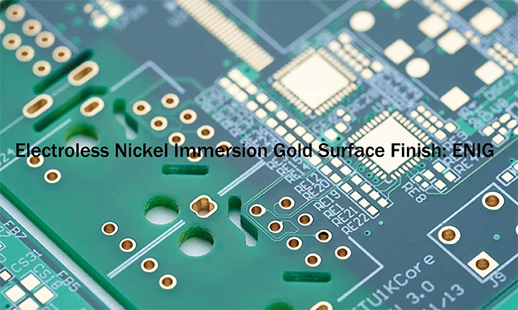
PCB Immersion Gold, also known as Electroless Nickel Immersion Gold (ENIG), is a surface finish used in the manufacturing of printed circuit boards (PCBs). It involves a two-step process that deposits a layer of electroless nickel on the PCB surface, followed by a layer of immersion gold.
The immersion gold process starts with the deposition of a thin layer of electroless nickel, which is achieved through a chemical reaction between the PCB surface and a nickel-phosphorus solution. The electroless nickel layer serves as a barrier between the copper traces on the PCB and the final gold layer.
After the electroless nickel deposition, the PCB is then immersed in a solution containing gold ions. The gold ions chemically react with the exposed surface of the electroless nickel layer, forming a thin layer of pure gold. The immersion gold layer is typically around 2-5 microinches thick.
Why Use Immersion Gold in PCB Manufacturing?
Many PCB manufacturers opt for immersion gold as the preferred option for fabricating circuit boards due to the superior solderability it offers compared to gold plating. While gold plating can exhibit poor solderability, immersion gold provides a reliable and robust solderable surface. This is primarily attributed to the flat and smooth surface finish achieved through the immersion gold process.
Additionally, the thin gold layer in immersion gold prevents the formation of intermetallic compounds during soldering, ensuring the creation of strong and dependable solder joints. As a result, immersion gold has become widely adopted in the electronics industry, particularly for applications involving printed circuit boards (PCBs).
There are several reasons why immersion gold is used in various applications:
Protection: Immersion gold provides a protective coating on the surface of a circuit board, preventing oxidation and corrosion. This coating helps to enhance the board’s durability and longevity.
Solderability: Immersion gold ensures excellent solderability, allowing for reliable and consistent solder joint formation during the assembly process. The gold surface creates a flat and smooth soldering area, reducing the risk of solder defects and ensuring good electrical connections.
Flatness and Planarity: Immersion gold creates a flat and even surface on the PCB, which is crucial for fine-pitch surface mount technology (SMT) components. This ensures proper component placement and alignment, leading to improved manufacturing yield and reliability.
Wire Bonding: Immersion gold is often used in applications that require wire bonding, such as integrated circuits and semiconductor packaging. The gold surface provides a suitable substrate for wire bonding, enabling reliable and low-resistance electrical connections.
Signal Integrity: The gold surface of immersion gold can improve signal integrity by reducing signal loss and impedance variations. This is particularly important for high-frequency applications, where any signal degradation can lead to performance issues.
Overall, immersion gold offers several advantages, including protection, solderability, flatness, wire bonding compatibility, and signal integrity, making it a preferred choice for many PCB manufacturers and electronic applications.
What are Some Limitations of ENIG Immersion Gold Surface Finish?
While immersion gold (ENIG) surface finish offers numerous advantages for optimal functionality of PCBs, it is important to acknowledge certain limitations associated with this particular finish:
1. Cost: ENIG surface finish is relatively expensive compared to other surface finishes available in the market. The additional processes involved in achieving the desired gold layer contribute to the higher cost of implementation.
2. Black Pad Syndrome: One of the drawbacks associated with ENIG is the occurrence of black pad syndrome. This phenomenon refers to the formation of a black, brittle layer between the nickel and gold layers, which can result in decreased solderability and reliability of the PCB.
3. Reworkability: ENIG surface finish is not well-suited for reworking. The gold layer, being relatively thin, can be easily compromised during rework processes such as desoldering and soldering, leading to potential damage to the finish and affecting the overall integrity of the PCB.
4. Sensitivity to Etching: ENIG surface finish can be susceptible to damage from etching processes. Harsh or prolonged etching can potentially degrade the gold layer, impacting the quality and functionality of the finish.
5. Signal Loss (RF): In certain high-frequency applications, such as RF (radio frequency), ENIG surface finish may exhibit signal loss due to its relatively higher surface roughness compared to alternative finishes like electroless nickel immersion gold (ENIPIG) or immersion tin.
6. Complex Process: The process of achieving ENIG surface finish is relatively complex compared to some other finishes. It involves multiple steps, including pretreatment, activation, and plating, requiring careful control and attention to detail during each stage.
While ENIG surface finish offers significant benefits, these limitations should be considered in the selection process, particularly when cost, reworkability, etching sensitivity, RF performance, and process complexity are important factors in the PCB manufacturing and application context.
Factors Influencing Immersion Gold (ENIG) Performance
Several factors can influence the performance of immersion gold (ENIG) as a surface finish on printed circuit boards (PCBs). These factors include:
Nickel Thickness:
The thickness of the electroless nickel layer in the ENIG process affects the overall performance. A thicker nickel layer provides better corrosion resistance and solderability but can lead to increased costs and potential issues with solder joint reliability. On the other hand, a thinner nickel layer may not provide sufficient protection against oxidation and corrosion.
Gold Thickness:
The thickness of the immersion gold layer also plays a significant role. A thicker gold layer offers better protection against oxidation and corrosion, but excessive gold thickness can result in solderability issues and increased costs. It is crucial to strike a balance between the desired level of protection and the compatibility with soldering processes.
Surface Smoothness:
The surface smoothness of the ENIG finish is critical for reliable soldering. A smooth surface ensures good solder wetting and adhesion, leading to robust solder joints. Surface roughness can result in poor solderability, solder bridging, or insufficient solder wetting, which can impact the overall performance and reliability of the PCB assembly.
Solder Joint Integrity:
The performance of ENIG can also be influenced by the quality and integrity of the solder joints formed during assembly. The surface finish should provide good solder wetting and adhesion, ensuring strong and reliable solder joints. Factors such as pad size, spacing, solder paste formulation, and reflow profile can also impact the solder joint quality and overall performance.
Environmental Conditions:
The performance of ENIG can vary depending on the operating environment of the PCB. Harsh conditions such as high humidity, temperature extremes, or exposure to chemicals can potentially degrade the surface finish over time. It is important to consider the expected environmental conditions and select a suitable surface finish that can withstand the intended operating environment.
Shelf Life and Storage Conditions:
The storage conditions and shelf life of ENIG-finished PCBs can also affect the performance. Proper handling, storage, and packaging practices should be followed to prevent contamination, oxidation, or damage to the surface finish during transportation and storage.
Manufacturing Process Compatibility:
The compatibility of ENIG with other manufacturing processes, such as solder mask application, assembly, and testing, is crucial. The surface finish should be compatible with the specific manufacturing processes used, ensuring proper adhesion, solderability, and reliability throughout the entire PCB manufacturing and assembly process.
Design Considerations for Immersion Gold (ENIG)
When designing a PCB with immersion gold (ENIG) as the surface finish, there are several important considerations to keep in mind:
Pad Size and Spacing:
ENIG has a relatively thick layer compared to other surface finishes. Therefore, it is important to adjust pad sizes and spacing accordingly to compensate for the additional thickness. Ensure that the pad sizes are compatible with the component’s soldering requirements and take into account the potential for solder paste bridging or insufficient solder wetting due to the thicker gold layer.
Annular Ring Width:
The annular ring refers to the copper area around a plated through-hole (PTH) pad. It is important to maintain an adequate annular ring width to ensure good solderability and mechanical reliability. The immersion gold layer can affect the size and strength of the annular ring.
Solder Mask Openings:
The solder mask is applied to the PCB surface to protect the copper traces and prevent solder bridging. When using ENIG, it is crucial to ensure that the solder mask openings are properly aligned with the pads to allow for accurate solder paste deposition during assembly. Misalignment can lead to soldering defects and affect overall reliability.
Component Placement:
ENIG provides a flat and smooth surface, making it suitable for fine-pitch surface mount technology (SMT) components. However, it is still important to carefully consider component placement to minimize the risk of solder bridging or tombstoning. Follow recommended design rules and guidelines for component spacing, keepout zones, and orientation to ensure proper soldering and avoid potential assembly issues.
Signal Integrity:
ENIG has excellent conductivity and can help maintain good signal integrity. However, it is important to consider the potential impact of the gold layer on high-frequency signals. The thickness and characteristics of the ENIG layer can affect impedance and signal propagation.
Handling and Storage:
Immersion gold is a delicate surface finish and can be susceptible to scratches and contamination. Proper handling and storage practices should be followed to prevent damage to the gold surface. Avoid excessive handling, use appropriate packaging materials, and store the PCBs in a controlled environment to maintain the integrity of the immersion gold finish.
By considering these design considerations, you can optimize the performance, reliability, and manufacturability of a PCB design using immersion gold (ENIG) as the surface finish.
The Difference Between Immersion Gold (ENIG) and Gold Plating
Immersion Gold (ENIG) and Gold Plating are two different methods of depositing a layer of gold onto the surface of a substrate. Here are the main differences between the two processes:
1. Process:
●Immersion Gold (ENIG): ENIG is a two-step process. First, a thin layer of nickel is deposited on the substrate surface, followed by a layer of gold. The nickel layer acts as a barrier between the substrate and the gold layer, preventing diffusion and ensuring good adhesion.
●Gold Plating: Gold plating is a single-step process where a layer of gold is directly plated onto the substrate surface.
2. Thickness:
●Immersion Gold (ENIG): The gold layer in ENIG is relatively thin, typically around 1-3 microinches (0.025-0.075 micrometers) in thickness.
●Gold Plating: Gold plating can vary in thickness depending on the application and requirements. It can range from a few microinches to several micrometers.
3. Surface Finish:
●Immersion Gold (ENIG): ENIG provides a flat and smooth surface finish. The gold layer is typically smooth and offers excellent solderability, making it suitable for soldering components.
●Gold Plating: Gold plating can have various surface finishes, including bright, matte, or satin. The choice of finish depends on the desired appearance and functionality.
4. Solderability:
●Immersion Gold (ENIG): ENIG offers good solderability due to the flat and smooth gold surface. The thin gold layer prevents the formation of intermetallic compounds during soldering, ensuring reliable solder joints.
●Gold Plating: The solderability of gold plating depends on the specific type and thickness of the gold layer. Proper selection and preparation of the gold plating can result in good solderability.
5. Cost:
●Immersion Gold (ENIG): ENIG is generally more expensive compared to gold plating due to the additional step of nickel deposition.
●Gold Plating: Gold plating is often less expensive than ENIG, as it involves a simpler plating process without the need for a nickel layer.
Both ENIG and gold plating have their advantages and are used in different applications. ENIG is commonly used in the electronics industry for printed circuit boards (PCBs) to provide a reliable solderable surface. Gold plating, on the other hand, is used in a wide range of applications, including jewelry, decorative items, electrical contacts, and connectors, where a thicker and more visually appealing gold layer is desired.
How to Create ENIG Surface Finish?
The surface finishing process for PCBs involves several key steps to ensure optimal performance and reliability. These steps can be summarized as follows:
1. Pretreatment: This initial stage involves the removal of oxides from the copper surface while simultaneously roughening it. The purpose of this step is to enhance the adhesion of subsequent layers, namely nickel and gold.
2. Micro Etching: In this step, a controlled etching process is employed to achieve a uniform and flat copper surface. This surface preparation is critical for ensuring proper adhesion and uniform deposition of subsequent layers.
3. Activation: To facilitate the deposition reaction, a layer of palladium (Pd) is applied to the copper surface. Palladium acts as a catalyst, promoting the reduction of palladium ions to form a palladium metal layer that adheres to the copper surface. This activation step prepares the surface for subsequent plating processes.
4. Nickel Plating: The next stage involves depositing a layer of nickel onto the activated copper surface. Nickel plating serves multiple purposes, including blocking diffusion between the copper and gold layers and providing a soldering base for improved solderability and robust interconnections.
5. Immersion Gold: Finally, the immersion gold step is implemented to prevent oxidation of the underlying nickel layer. An immersion gold bath is used to deposit a thin layer of gold onto the nickel-plated surface, providing excellent solderability, corrosion resistance, and a visually appealing finish.
These sequential processes, from pretreatment to immersion gold, ensure the formation of a reliable and functional surface finish on the PCB, offering protection against oxidation, promoting solderability, and facilitating optimal electrical performance.
What Problems often Occur in the Process of Immersion Gold of the Circuit Board?
Several problems can occur during the immersion gold (ENIG) process of circuit board manufacturing. Some common issues include:
Nickel Pitting: During the electroless nickel deposition step, nickel pitting can occur, leading to an uneven or rough surface. This can result from inadequate cleaning or contamination on the board surface, improper bath chemistry, or incorrect process parameters. Nickel pitting can affect the overall surface smoothness and solderability of the ENIG finish.
Incomplete Gold Deposition: In some cases, the gold layer may not deposit uniformly or adequately over the nickel layer. This can result in patchy or uneven gold coverage, leading to solderability issues and potential reliability problems. Insufficient gold deposition can be caused by factors such as inadequate activation of the nickel surface, improper gold bath chemistry, or process parameter deviations.
Black Pad: Black pad is a defect characterized by the formation of a black or dark-colored layer between the nickel and gold layers. It occurs due to excessive surface oxidation of the nickel layer before gold deposition. Black pad can lead to poor solderability, reduced adhesion, and potential solder joint failures.
Gold Peeling or Delamination: In some cases, the gold layer can peel or delaminate from the underlying nickel layer. This problem can arise due to poor adhesion between the gold and nickel layers, inadequate surface preparation, or improper process control. Gold peeling or delamination can result in solderability issues, reduced reliability, and potential electrical failures.
Surface Contamination: Contamination of the ENIG surface can occur during various stages of the process, such as handling, cleaning, or rinsing. Contaminants like oils, fingerprints, dust particles, or residual chemicals can impact the quality of the surface finish. Surface contamination can lead to solderability issues, poor adhesion, or reliability problems.
Surface Roughness: ENIG surfaces should have a smooth and uniform appearance. However, surface roughness can occur due to factors such as improper cleaning, inadequate activation, or problems in the nickel or gold deposition process. Surface roughness can adversely affect solderability, lead to solder bridging, or result in poor solder joint formation.
Corrosion: ENIG surfaces are generally resistant to oxidation and corrosion. However, certain conditions, such as exposure to high humidity or harsh chemicals, can lead to corrosion of the gold layer. Corrosion can affect the overall performance and reliability of the PCB assembly.
To minimize these problems, it is crucial to follow proper process controls, adhere to recommended process parameters, conduct regular process monitoring and inspection, and ensure the use of high-quality materials and chemicals. Additionally, effective cleaning and surface preparation practices, as well as strict adherence to industry standards and guidelines, can help mitigate these issues during the immersion gold process.
Conclusion
Electroless nickel immersion gold (ENIG) has emerged as a highly popular surface finish in the PCB industry, offering numerous advantages that make it an excellent choice for manufacturers. Among the various surface finishes available, ENIG is widely preferred and adopted.
ENIG’s key advantage lies in its ability to provide a protective nickel layer that acts as a barrier between the underlying copper and the final gold layer. This feature not only ensures reliable interconnections but also contributes to its environmentally-friendly profile, making it an attractive option for PCB manufacturers seeking sustainable solutions.
However, it is important to note that ENIG, like any other surface finish, has its limitations and considerations. This comprehensive article delves into the intricacies of electroless nickel immersion gold, exploring its benefits, drawbacks, and providing valuable insights for PCB manufacturers and professionals in the field.

