
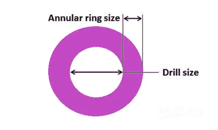
In the process of manufacturing a printed circuit board (PCB), drilling holes is a crucial step for creating through-hole technology and vias that connect traces in multilayer circuits. This involves precisely piercing a hole through the center of a copper pad to create what is known as an annular ring. The annular ring is the remaining circular area of the pad after drilling.
To ensure compliance with international PCB manufacturing standards, precision is of utmost importance when drilling holes in a PCB. This is crucial for the successful fabrication and optimal functioning of the PCB. Hence, it is imperative to consider essential design aspects of annular rings and how they operate in the drilling process to achieve satisfactory results.
What Is an Annular Ring on PCBs ?
In PCB manufacturing, the annular ring refers to the copper pad’s area surrounding a drilled hole or a copper-plated via. In a multilayer PCB, there must be enough copper around the via to ensure a reliable connection between the via and copper traces. The primary purpose of an annular ring is to establish a dependable connection between the via and the copper trace for optimal circuit performance and functionality. This is a critical design consideration for multilayer PCBs, and it is crucial to meet the required standards for reliable and efficient PCB fabrication.
The annular ring plays a pivotal role in providing a location for the connection of leads or wires to the electrical component, acting as a pivot point for the circuit. In PCB design engineering, the minimum diameter of the holes is determined by the expertise of the manufacturer in the PCB assembly process. This skillset is influenced by various factors such as the nature of the holes and whether they are plated or not. Achieving the desired hole diameters, surface finish, and plating all rely heavily on the expertise of the manufacturer. As a result, PCB design engineers should collaborate closely with highly skilled manufacturers with PCB assembly experience to ensure the reliable functionality of the PCB.
Types of Annular Ring
There are several types of annular rings used in PCB design, including:
● Through-hole annular rings: These are used in traditional through-hole PCB designs, where components are inserted into holes drilled through the board and soldered on the other side.
● Surface mount annular rings: These are used in surface mount technology (SMT) designs, where components are mounted directly on the surface of the board without the need for through-holes.
● Microvia and Blind/Buried via annular rings: These are used in advanced PCB designs for high-density interconnects (HDI), where smaller vias are drilled and filled with conductive material to create connections between layers.
● Stacked vias annular rings: These are used to connect multiple layers of a PCB, where multiple vias are stacked on top of each other to create a single connection.
Factors Affecting Annular Rings
The factors affecting annular rings in PCB design include:
● Hole size and placement: The size of the drilled hole and its position relative to the trace can affect the annular ring’s size and shape.
● Trace width: The width of the trace connected to the pad affects the annular ring size. Wider traces require larger annular rings.
● Copper thickness: The thickness of the copper layer on the PCB affects the annular ring size, and thicker copper layers require larger annular rings.
● Board material and manufacturing process: The choice of PCB substrate and the manufacturing process used can affect the quality and consistency of the annular ring
The annular ring offers a location for the connection of leads or wires to the electrical component, which acts as a pivot point for the circuit. The manufacturer’s skills for PCB assembly, which can differ depending on the nature of the holes and whether or not they are plated, will be the determining factor in determining the minimum diameter of the holes.
PCB Annular Ring Design Tips
In PCB manufacturing, the annular ring’s specifications and guidelines are regulated by the rules and standards governing the board’s construction. These standards are set out in the IPC-2221 Generic Standard on Printed Board Design, the IPC-A-600 Acceptability of Printed Boards, and the IPC-6012 Qualification and Performance Specification for Rigid Printed Boards. The industry classification of the PCBA’s application will typically determine the minimum acceptance dimension or lowest tolerance required to meet these standards.
To ensure compliance, adhering to the outlined procedures and standards is critical in producing quality PCBs that meet the applicable regulations. By following the appropriate regulations and utilizing skilled manufacturing expertise, design engineers can produce high-quality PCBs that meet necessary standards for reliable and efficient circuit performance.
PCB design engineers must take specific actions when designing a PCB with annular rings to ensure that the final product meets the necessary standards and guidelines. These include identifying the IPC class that the board falls under and the associated development guidelines, determining the required annular ring clearance, the minimum annular ring width, and the minimum via wall (if applicable). Establishing the annular ring size and placement is also crucial in achieving optimal circuit functionality.
To ensure successful PCB design, the parameters must be within the tolerances of the DFM standards and guidelines of the contract manufacturer (CM). Failure to comply with these standards may result in issues such as breakout, which occurs when the drill hole extends beyond the annular ring, solder bridging, or solder mask expansion. Therefore, adhering strictly to the guidelines and standards is crucial for producing high-quality PCBs that meet the necessary technical specifications for reliable and efficient circuit performance.
PCB Annular Ring Design Process
Here’s a general process for designing a PCB annular ring:
● Determine the drill size: The annular ring size is determined by the drill size used to create the hole in the PCB.
● Determine the pad size: The diameter of the pad should be larger than the drill diameter to ensure sufficient copper area for electrical connectivity and mechanical stability.
● Determine the annular ring diameter: The annular ring diameter is the difference between the pad diameter and the drill diameter. It should be wide enough to provide adequate copper area for mechanical stability and solderability but narrow enough to avoid interfering with other traces or components on the board.
● Determine the annular ring width: The annular ring width is the distance between the edge of the drill hole and the edge of the pad. It should be wide enough to provide sufficient copper area for mechanical stability and solderability.
● Consider copper weight and trace clearance: The copper weight and trace clearance should be taken into account to ensure adequate current carrying capacity and to prevent short circuits.
● Determine annular ring placement: Place the annular ring in a location that does not interfere with other components or traces on the PCB.
● Review the design: Review the design to ensure that the annular ring meets the necessary design requirements, such as mechanical stability, electrical connectivity, and manufacturability.
PCB Annular Ring Width: How do You Calculate ?
PCB designers share a crucial responsibility in ensuring the appropriate size of annular rings to ensure the reliable and efficient functionality of the PCB. Incorrect annular ring sizes can negatively impact the operation of the entire PCB, highlighting the importance of designers to specify the appropriate ring sizes to manufacturers.
Designers can use a formula to calculate the width of an annular ring, which is calculated by subtracting the diameter of the hole from the diameter of the pad and dividing by 2.
For example
If the diameter of the pad is 22 mils and the diameter of the hole is 10 mils, the annular ring width can be calculated as (22-10)/2, which is equal to 6 mils.
Conversely, if a designer knows the annular ring width of a particular pad, it is feasible to deduce that the pad’s diameter will be twice the annular ring width larger than the hole’s diameter.
Therefore, PCB designers have a crucial role in determining the correct annular ring sizes for optimal PCB design, and calculations using the appropriate formula are essential to produce circuits that are both functional and of the highest quality.
PCB Minimum Annular Ring: Calculation Formula
Calculating the size of the annular ring in a PCB isn’t as complex as many people believe it to be, yet many designers are unfamiliar with its computational method. When constructing vias, it is necessary to have copper surrounding the drilled holes. This copper ring, known as the outside diameter, represents the via size.
To calculate the minimum annular ring size in accordance with IPC-2221A specifications, PCB design engineers should follow the steps outlined below:
● Determine the drill hole size.
● Identify the minimum clearance required between the drill hole and the copper pour.
● Determine the minimum trace width requirement.
● Use the formula [(2 x [minimum clearance + minimum trace width] + drill hole size] / 2 to calculate the minimum annular ring size.
Applying the IPC-2221A specifications and formula to calculate the minimum annular ring size is essential in producing high-quality PCBs that meet the necessary technical requirements for optimal circuit functionality.
Minimum Annular Ring
Both the internal and external layers of a PCB have their own minimum annular ring standards. Generally, the standard minimum annular ring for inner layers is 0.1 mm, while for external layers, it is 0.05 mm.
However, creating small annular rings based on tight spacings of surrounding components may increase the likelihood of drilled vias being close to the ring’s edges. This increases the risk of the via separating from the annular ring, resulting in a severed trace link, which compromises the functionality of the PCB. These scenarios can result in brittle connections and hamper the circuit’s performance.
While a 1 mil diameter annular ring is technically feasible, it is not recommended due to the increased likelihood of a breakthrough. Therefore, it is critical for PCB design engineers to ensure that the minimum annular ring diameter adheres to the necessary technical criteria. This will prevent risk factors such as via separation, potential circuit failure disruption, and ensure high PCB standards adhering to industry guidelines.
Why Size Is Important to PCB Annular Ring ?
For PCB manufacturers, ensuring a secure electrical connection with the via is crucial to produce a high-quality circuit. The annular ring’s thickness must be of adequate breadth to guarantee a reliable electrical connection. To meet the design requirements, it is recommended that the ring’s minimum length be equal to or greater than the width stated, as any dimension smaller than the specified value could cause issues with component attachment.
If the annular ring’s length is too small, this can result in pad breakout, also referred to as zero annular ring, which is typically related to the circuit’s pad entry location. If this issue goes untreated, it could lead to a decrease in the circuit’s current-carrying capability, which would affect the PCB’s overall functionality.
Therefore, it is crucial for PCB manufacturers to adhere to the design specifications and utilize the appropriate dimensions for the annular ring, guaranteeing a secure electrical connection with the via and preventing any potential issues such as pad breakout. By ensuring the proper technical specifications are met, manufacturers can produce a high-quality PCB that meets industry standards and performs efficiently.
PCB Annular Ring: How to Get the Size Right ?
The PCB manufacturer provides a tolerance for the annular ring during the PCB manufacturing process. It is recommended that designers add a small amount of additional space to err on the side of caution, even with specified tolerances.
Most designers suggest expanding the annular ring size by 1mm compared to the manufacturer’s specifications. This slight increase in width can be beneficial in resolving potential future issues. By adding extra space to the design, the risks of component attachment problems or other issues during the PCB manufacturing process are lowered. Hence, design engineers must ensure that the annular ring size is not only within the specified levels given by the manufacturer but also sufficient so that performance issues will not occur after the product is fabricated.
Decide the Dimensions Based on Your Application
Printed circuit boards (PCBs) are widely used in various industries, including medical, military, and domestic appliances, due to their high thermal capabilities and excellent insulating qualities. Hence, it is vital to consider the final application of the PCB during annular ring estimation.
The specifications for annular rings may vary depending on the intended use, and for applications such as military equipment, superior quality annular rings may be required. PCBs are classified into three levels, namely: level 1, level 2, and level 3. Class 3 annular ring specifications differ from Classes 1 and 2 since Class 3 boards are designed for more heavy-duty applications. Typically, the pad size required for accommodating the via diameter in Class 3 PCBs is larger compared to classes 1 and 2.
It is important for PCB manufacturers to consider and adhere to the necessary technical criteria, such as the application and class of the PCB, while estimating the annular ring. By following the applicable specifications for the PCB class and end use, manufacturers can create high-quality PCBs that perform optimally. This ensures that the PCBs meet the required standards and can be used in specific applications such as military equipment.
PCB Annular Ring Vs. Though-Hole
There is often confusion between the PCB annular ring and the via through-hole, despite the two being distinct concepts. The annular ring refers to the area between the copper pad and the via’s edge. A wide annular ring width is necessary to ensure strong connections for the vias. Typically, the annular rings for most PCBs have precise width measurements.
On the other hand, the through-hole technique is a method used for mounting electronic components. This procedure involves soldering leads to materials that are then inserted into drilled holes in the PCB. It is a simple and effective process that is less likely to produce errors and is thus suitable for PCB design enthusiasts to use.
PCB design engineers must recognize the differences between annular rings and through-holes. Precisely defining the annular ring and employing the correct dimensions is critical to maintaining a solid electrical connection in the PCB. Meanwhile, through-hole plating techniques can be used to improve the connections of components that will be mounted on the PCB. By understanding these key design principles, engineers can create a well-designed and functional PCB that meets the necessary standards.
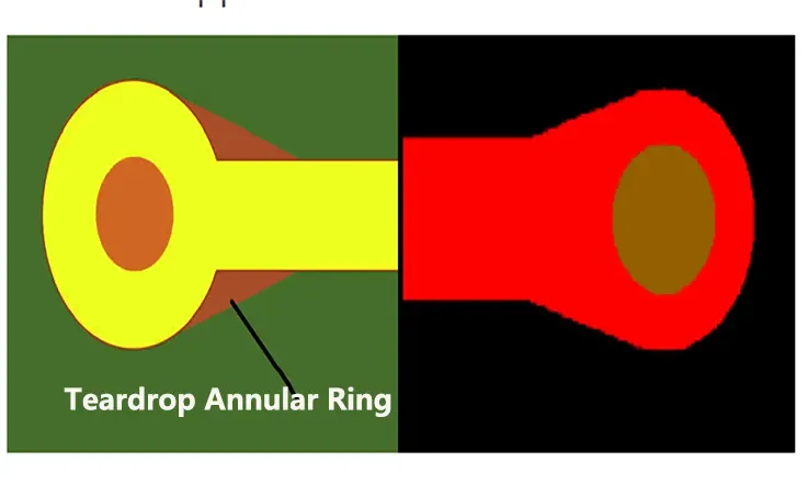
What Is the Teardrop Annular Ring ?
In the realm of PCB design, the shape of a teardrop is often utilized to create an annular ring. Rather than constructing a conventional circle, the designer adds supplementary copper to join the edges of the ring. This technique bestows increased durability upon the ring due to the additional copper reinforcement.
One of the most frequent scenarios necessitating the implementation of teardrop annular rings is when the drill bit deviates ever so slightly from its intended path during the hole drilling process. This deviation can result in the removal of an excessive amount of copper, leaving the connection vulnerable.
Advantages of Teardrop annular rings
● Improved reliability: By reinforcing the connection between the pad and the trace with additional copper, teardrop annular rings provide greater mechanical strength, minimizing the risk of connection failure caused by thermal stress, vibration, or other environmental factors.
● Enhanced manufacturability: In cases where the drill bit may deviate from the intended path during the drilling process, teardrop annular rings can prevent damage to the copper and provide a more robust connection, improving the overall yield and reducing manufacturing costs.
● Increased design flexibility: Teardrop annular rings allow for greater design flexibility, enabling the designer to place components or traces closer together than might otherwise be possible.
Better signal integrity: The additional copper used in teardrop annular rings helps to ensure better signal integrity by reducing the impedance and improving the connection between the pad and the trace, resulting in less signal loss and distortion.
Common Annular Ring Issues
There are several common issues that can arise with annular rings in PCB design, including:
● Insufficient annular ring width: If the width of the annular ring is too narrow, it can weaken the connection between the pad and the trace, making it more vulnerable to damage or failure.
● Annular ring breakout: This occurs when the drill bit deviates too far from the intended path, causing the copper to break out or fracture, which can result in a weakened or broken connection.
● Annular ring slivers: Small, thin pieces of copper or other debris can sometimes become stuck in the annular ring during the drilling or plating process, causing a short circuit or other electrical issues.
● Annular ring voids: These are areas within the annular ring where the copper plating has not adhered correctly to the substrate, resulting in a weaker or incomplete connection.
To avoid these issues, it is essential to carefully consider the size and placement of annular rings during the PCB design process, and to perform regular inspections and quality control measures during fabrication and assembly.
The Importance of the Drilling Accuracy
In PCB design, precise drilling is crucial, particularly with smaller and densely populated boards, to reduce the size of annular rings. By utilizing an annular ring, a reliable electrical connection can be established even if the via is not centrally located within the ring. As long as the annular ring contacts the pad boundary yet remains inside it, the connection is deemed satisfactory.
Engineers may sometimes design very small annular rings when there is minimal space between adjacent components. However, this increases the possibility of having vias located much too close to the edge of the ring, leading to an annular ring breakout. Therefore, PCB manufacturers should ensure precise and accurate annular ring formation, while PCB designers should leave adequate margains to accommodate additional tolerance values to achieve satisfactory results.
At JarnisTech, the minimum width of an annular ring is 0.15 mm, while the drill size ranges from 0.2 mm to 6.3 mm. However, if the via size exceeds its acceptable range, an additional cost may be incurred. Therefore, it is advisable to learn more about the manufacturing tolerance values before initiating an order.
In PCB design, it is essential to maintain a minimum distance between annular rings and ensure sufficient via space to avoid disruption of the electrical connection. At JarnisTech, we provide pertinent advice that matches your PCB design needs, whether it is for PCB prototype assembly or small batch production. Count on us for professional services.

How Can JarnisTech Team Help You ?
At JarnisTech, we offer a comprehensive range of PCB services to our clients, making us one of the most dependable and reputable businesses in the industry. We strive to stand out from the competition by providing our clients with expert assistance in resolving any PCB-related issues that they may encounter.
We take pride in being a one-stop destination for all PCB requirements and are capable of providing high-quality PCB boards that are both produced and assembled with precision. Our ability to offer a wide variety of PCB services ensures that our clients have access to the most efficient and effective solutions for their project needs.
If you are searching for a reliable and professional source for all your PCB requirements, look no further than JarnisTech. We are committed to delivering the highest standards of quality and service to our clients, and we welcome the opportunity to be your trusted partner for all your PCB needs.
Future Outlook of Annular Ring
In terms of future outlook, advancements in materials and manufacturing processes are leading to smaller, more compact PCB designs, with higher component densities and faster signal speeds. This trend is driving the need for more precise and accurate annular ring designs, placing even greater importance on their optimization and implementation.
Additionally, the increasing demand for flexible and wearable electronics is also driving innovation in annular ring design, as these devices have unique requirements and constraints that must be carefully considered. Overall, the future of PCB annular rings is likely to be characterized by continued innovation, optimization, and miniaturization.
Conclusion
An annular ring is a copper pad that surrounds a via on a printed circuit board. It serves a crucial role in PCB functionality by facilitating robust connections between the via and traces. Without annular rings, the via would be unable to carry signals effectively. Thus, it is essential to consider annular ring width and tangency to avoid breakout defects during the PCB manufacturing process.
If you require high-quality printed circuit boards with recommended annular ring specifications, JarnisTech offers some of the best options in the market. Our products are designed to reduce tangency and prevent breakout defects, providing reliable functionality to suit your application. Don’t hesitate to contact us to learn more about the comprehensive range of services we provide, each tailored to meet your PCB needs.
Related Posts:
1. What Is PCB Etching and How to Make a perfect PCB Etching?
2. The Best PCB Panelization Guide
3. The Importance of 3D Printed PCBs in Modern Electronics Production
4. Understanding PCB Delamination: A Comprehensive Guide
5. The Best Backplane Printed Circuit Boards Factory
6. An Overview of Through-hole Technology (THT)
7. Detail Talk Surface Mount Technology
8. PCB Clone : Copy Your Printed Circuit Board
9. PCB Drilling: Definition, Technology Types and Process
10. Castellation PCB Fabrication: Castellated Hole (Plated Half Hole) Technologys Why So Important


