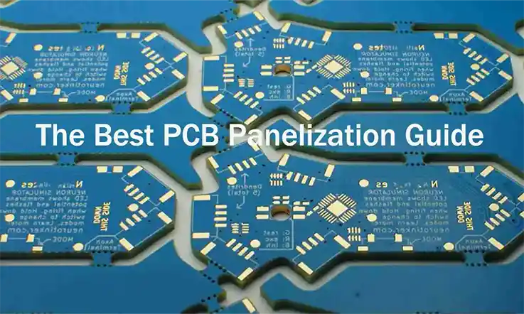
Printed Circuit Board (PCB) panelization is a critical step in the electronics manufacturing process that plays a significant role in optimizing efficiency and cost-effectiveness. As electronic devices become more compact and complex, the demand for smaller and more intricate PCB designs continues to rise. To meet these demands, manufacturers employ panelization techniques to efficiently produce multiple PCBs on a single panel.
This article aims to explore the impact of panelization design on PCB fabrication, emphasizing its importance and offering valuable insights for achieving optimal design.
What is PCB Panelization?
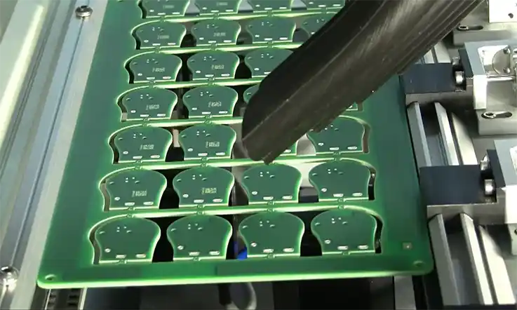
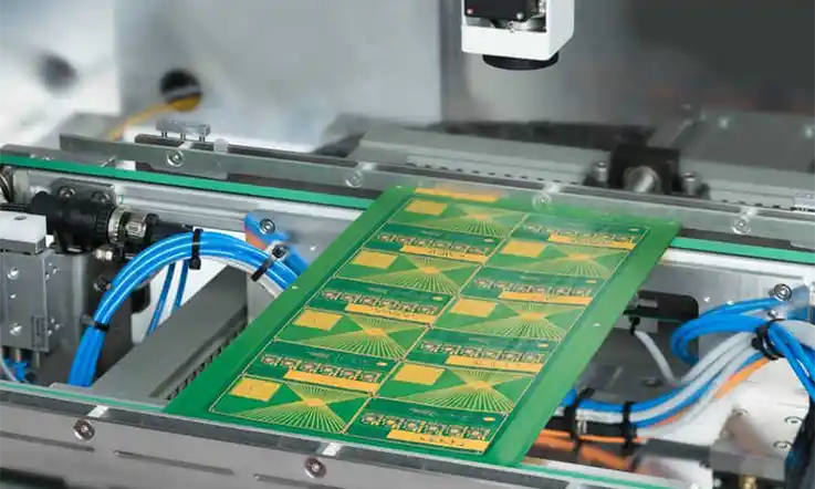
PCB panelization is a manufacturing technique that involves producing multiple smaller boards interconnected as a single array, facilitating efficient movement through the assembly line. Depanelization allows individual boards to be separated from the array for packaging or installation into products. Another approach involves adding a processing edge around each board to increase its width for compatibility with the assembly line.
To fully leverage the advantages of mass production through panelization, it is crucial to consider the following design factors:
PCB array strength: Achieving a balance between easy depanelization and maintaining array integrity during production is essential. Increasing the number of boards per array enhances strength and reduces vibration.
Component layout: Careful consideration should be given to the placement of components and connectors, particularly those extending beyond the board’s edge. This is especially important for sensitive SMT components located near the board’s edge.
PCB shape: The shape of the board can complicate the panelization process. Ideally, rectangular boards are preferred. However, if the board has a complex shape, alternating images from 90° to 180° can help optimize space on a panel. Utilizing a CAD program can assist in fitting unusually shaped boards into an array.
Tooling holes: Arrays and break-away processing edges can provide space for tooling holes, which are crucial for automated testing on the assembly line.
By considering these design considerations, PCB panelization can enhance the efficiency of fabrication and assembly processes, enabling streamlined mass production and improved overall product quality.
PCB Panelization Design Method
When it comes to PCB panelization design, there are several methods and techniques that can be employed to achieve optimal results. Here are some commonly used approaches:
Grid-Based Panelization
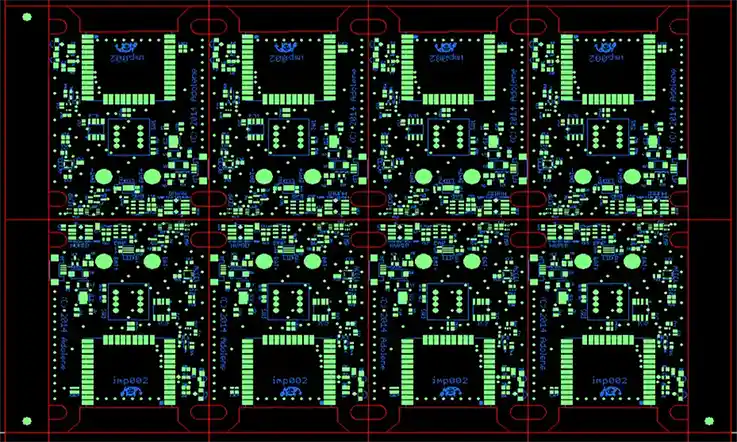
This method involves arranging PCBs in a grid pattern on a panel. The boards are evenly spaced and aligned to facilitate efficient manufacturing and assembly processes. Grid-based panelization is straightforward and allows for easy handling and depanelization.
Tab Routing
Tab routing involves adding small tabs or bridges between individual PCBs on a panel. These tabs provide mechanical support during manufacturing and allow for easy separation of the boards after assembly. Tab routing is often used when the PCBs are of a similar size and shape.
Breakaway Rails
Breakaway rails are additional sections of material added around the perimeter of the panel, creating a larger panel size. The individual PCBs are located within these rails and can be easily separated after manufacturing. Breakaway rails provide stability and support during fabrication and assembly.
Mouse Bite Panelization
In this method, small perforations or mouse bites are created between individual PCBs, allowing for easy separation. Mouse bites are small, partially cut sections that can be easily snapped or broken to separate the boards. This method is commonly used when space constraints are a concern.
V-Scoring

V-scoring involves creating V-shaped grooves on the panel between the individual PCBs. These grooves allow for easy separation by bending the panel along the scored line. V-scoring is particularly useful when working with larger boards or when a clean and precise separation is desired.
Panel Array Design
In this approach, multiple PCBs of the same design are replicated and placed side by side on a larger panel. This method maximizes production efficiency by allowing for simultaneous manufacturing and assembly of multiple boards.
The choice of panelization design method depends on factors such as PCB size, quantity, shape, assembly requirements, and desired level of automation. It is important to consider the specific needs of the project and consult with PCB manufacturing experts to determine the most suitable panelization method for optimal fabrication and assembly results.
V-score vs. Tab Routing PCB Panels
The decision of whether to use V-scoring or tab routing for a PCB panel depends on the specific design considerations for that board. While these two methods are not mutually exclusive and can be combined when appropriate, there are tradeoffs to weigh for each one.
V-scoring is generally a faster process than tab routing, requiring less time on the routing machine. However, tab routing may provide higher edge quality, with only small laminate nubs that can be easily sanded off to leave smooth edges. In contrast, V-scoring tends to leave rougher edges across the board.
The shape of the PCBs in the panel should be evaluated when selecting the panelization method. V-scoring performs well for square or rectangular boards, while tab routing accommodates more irregular board outlines.
If the design has components placed near the board edges, tab routing may be preferable to avoid damaging these components, provided the tabs themselves are not positioned too close to the edges.
Finally, V-scoring is the more material-efficient technique, producing less waste than tab routing. This can significantly reduce costs on a per board basis.
By weighing these factors against the specific needs of the PCB design, engineers can make an informed decision between V-scoring and tab routing to optimize the panelization process. A combination approach is also possible when elements of both methods would benefit the board layout.
When is PCB Panelization Required?
PCB panelization is typically required in the following situations:
Mass Production: When producing PCBs in large quantities, panelization is necessary to optimize the manufacturing process. By arranging multiple boards on a single panel, efficiency is improved, as it allows for simultaneous fabrication and assembly of multiple PCBs.
Cost-Effectiveness: Panelization offers cost savings in terms of materials, setup, and handling. By maximizing the use of manufacturing equipment and minimizing material waste, panelization helps reduce production costs, making it a preferred method for cost-effective PCB manufacturing.
Assembly Line Compatibility: PCBs that need to be processed through automated assembly lines often require panelization. By designing the panel layout to match the assembly line’s capabilities, it ensures smooth and efficient automated assembly processes.
Space Optimization: Panelization is useful when trying to optimize the utilization of available space on a production panel. By arranging PCBs strategically, designers can maximize the number of boards that can fit on a single panel, minimizing wasted space.
Handling and Transportation: Panelization simplifies the handling and transportation of PCBs. By keeping multiple boards connected on a panel, they can be easily moved as a single unit, reducing the risk of damage or misplacement during transit.
Depanelization Requirements: If individual PCBs need to be separated from the panel after fabrication and assembly for packaging or installation purposes, panelization is necessary. It allows for controlled and efficient depanelization processes, ensuring the integrity of the individual boards.
It is important to consider the specific production requirements, quantity, and desired outcomes when determining whether PCB panelization is necessary. Consulting with PCB manufacturers and considering factors such as manufacturing capabilities, cost-efficiency, and logistics can help determine the need for panelization in a particular project.
Design Considerations for PCB Panelization
When designing PCB panelization, there are several important considerations to take into account to ensure a successful and efficient manufacturing process. Here are some key design considerations for PCB panelization:
Board Orientation and Alignment
Ensure that the PCBs are properly aligned and oriented within the panel. Consistent alignment helps maintain uniformity throughout the manufacturing process and facilitates accurate component placement and assembly.
Panel Size and Material
Determine the appropriate panel size based on the PCB dimensions and manufacturing requirements. Consider the material used for the panel, such as FR-4 or aluminum, and its compatibility with the PCB fabrication and assembly processes.
Spacing and Clearances
Provide adequate spacing between PCBs on the panel to prevent electrical and mechanical interference. Consider the clearance requirements for components, connectors, and traces that extend beyond the board edges. Adhere to design rules and industry standards to ensure proper functionality and reliability.
Tooling Holes and Fiducial Marks
Incorporate tooling holes into the panel design to facilitate accurate registration and alignment during manufacturing processes, such as drilling, routing, and assembly. Include fiducial marks for automated optical inspection (AOI) and component placement accuracy.
Breakaway Tabs or V-Grooves
If using breakaway tabs or V-grooves for depanelization, carefully design their placement to ensure easy separation without damaging the PCBs. Consider the size and quantity of tabs or grooves needed for proper mechanical support during manufacturing and easy separation afterward.
Panelization Method Selection
Choose the most suitable panelization method based on the PCB design and manufacturing requirements. Consider factors such as board size, shape, assembly process, and depanelization needs. Evaluate the advantages and limitations of different panelization methods to optimize efficiency and minimize waste.
Design for Assembly (DFA)
Design the panelization layout with assembly in mind. Group components with similar functionalities or assembly processes together to minimize assembly time and improve efficiency. Consider the accessibility of components for automated assembly equipment, such as pick-and-place machines.
Design for Testing
Plan for efficient testing and inspection of the PCBs within the panel. Ensure that test points are accessible and properly positioned for automated or manual testing methods. Consider the placement of test pads, test points, or test vias for electrical testing and debugging purposes.
Documentation and Communication
Clearly document and communicate the panelization design to PCB manufacturers and assembly partners. Provide comprehensive manufacturing instructions, including panelization drawings, assembly data, and any specific requirements or considerations for successful production.
By considering these design considerations during the PCB panelization process, you can optimize the manufacturing efficiency, assembly quality, and overall success of your PCB production. Collaborate closely with PCB manufacturers and assembly partners to ensure alignment with their capabilities and requirements.
How to Process the PCB Panelization design?
The process of PCB panelization design involves several key steps to ensure a successful outcome. Here is a general outline of the process:
1. Determine Panel Size and Quantity: Start by determining the desired panel size based on the PCB dimensions and manufacturing capabilities. Consider factors such as machine limitations, handling requirements, and production efficiency. Decide on the number of PCBs to be included in each panel based on production volume and cost considerations.
2. Define Panelization Method: Choose the appropriate panelization method that suits your project requirements. Consider factors such as board size, shape, assembly process, and depanelization needs. Common methods include grid-based panelization, tab routing, breakaway rails, mouse bite panelization, V-scoring, or panel array design.
3. Create Panelization Layout: Using a PCB design software or a dedicated panelization tool, create a panelization layout that arranges the PCBs on the panel according to the chosen method. Take into account the required spacing between boards, alignment, and any additional features like tooling holes or fiducial marks. Ensure that the layout adheres to design for manufacturability (DFM) guidelines.
4. Consider Component Placement: Pay attention to component placement on the PCBs within the panel. Avoid placing sensitive components near the panel edges or areas prone to stress during depanelization. Ensure proper clearance for connectors and other components that extend beyond the board edges.
5. Verify Design Rules and Constraints: Before finalizing the panelization design, run design rule checks (DRC) to ensure that the layout conforms to manufacturing and assembly requirements. Verify that there are no violations related to spacing, copper clearances, solder mask, or silkscreen markings.
6. Generate Panelization Files: Once the panelization design is complete, generate the necessary files for manufacturing. This usually includes Gerber files, NC drill files, assembly data, and any additional documentation or instructions required by the manufacturer.
7. Collaborate with PCB Manufacturer: Engage in communication and collaboration with the chosen PCB manufacturer. Share the panelization design files and discuss any specific requirements or recommendations. Seek their expertise to ensure the design is optimized for their manufacturing capabilities.
8. Review and Iteration: Review the panelization design with the manufacturer and address any feedback or modifications required. Iterate on the design if necessary to achieve the desired manufacturability, assembly efficiency, and cost-effectiveness.
By following these steps and collaborating closely with the PCB manufacturer, you can effectively process the PCB panelization design and ensure a smooth transition from design to production.
The Effect of Panelization Design on PCB Fabrication and Assembly
Panelization is an important aspect of Printed Circuit Board (PCB) manufacturing that involves the process of arranging multiple PCBs onto a larger board, or panel, during fabrication. The panel is then broken apart into individual PCBs after assembly. This process allows for the simultaneous fabrication and assembly of multiple PCBs, improving overall efficiency and reducing costs. However, the design of the panel can influence various factors in PCB fabrication and assembly, including cost, manufacturability, and reliability.
Efficiency and Cost-Effectiveness
Panelization design can significantly influence the efficiency and cost-effectiveness of PCB production. A well-designed panel can maximize the number of PCBs on a single panel, reducing material waste and lowering production costs. Furthermore, by allowing for the simultaneous processing of multiple boards, panelization can increase production speed and reduce labor costs.
Manufacturability
The design of the panel can also affect the manufacturability of the PCBs. For instance, boards that are too closely spaced may be difficult to route or may result in damaged boards when depaneling. On the other hand, too much space between boards can lead to wasted material and increased costs. Additionally, the panel design should also consider aspects such as the placement of fiducial marks and tooling holes, which can influence the accuracy and ease of assembly.
Reliability
Panelization design can impact the reliability of the final PCBs. For example, inadequate spacing or poorly designed break-off tabs can lead to damage during depaneling, potentially affecting the functionality and reliability of the PCBs. Moreover, the panel design should ensure that it can withstand the stresses of assembly processes, such as soldering and component placement, without warping or breaking.
Design for Manufacturability (DFM)
Panelization is an important aspect of Design for Manufacturability (DFM) in PCB production. DFM involves designing the PCB in a way that optimizes its manufacturability, considering factors such as ease of fabrication, assembly, testing, and cost-effectiveness. A well-designed panel can improve all these aspects, leading to a more efficient and cost-effective production process.
Therefore, panelization design plays a crucial role in PCB fabrication and assembly, affecting factors such as efficiency, cost-effectiveness, manufacturability, and reliability. Therefore, it’s important to carefully consider the design of the panel in the early stages of the PCB design process.
Conclusion
The significance of panelization design on PCB fabrication and assembly cannot be overstated. A carefully planned panelization design has a profound impact on the manufacturing process, improving efficiency, assembly, testing, and resource utilization. By integrating the specific requirements of PCB fabrication and assembly into the design process, engineers can achieve a streamlined and cost-effective production, resulting in high-quality PCBs suitable for a wide range of applications.
At JarnisTech, we are proud to offer our exceptional PCB panelization services to a global customer base. With our highly skilled and experienced team of professionals, we assure you that all your PCB panelization needs will be catered to with utmost care and precision. Whether you require panelization for small-scale projects or large-scale production, we have the expertise to deliver outstanding results. Contact us today to request a quote and experience the quality and efficiency of our PCB panelization services.
Related Posts:
1. What Is PCB Etching and How to Make a perfect PCB Etching?
3. The Importance of 3D Printed PCBs in Modern Electronics Production
4. Understanding PCB Delamination: A Comprehensive Guide
5. The Best Backplane Printed Circuit Boards Factory
6. An Overview of Through-hole Technology (THT)
7. Detail Talk Surface Mount Technology