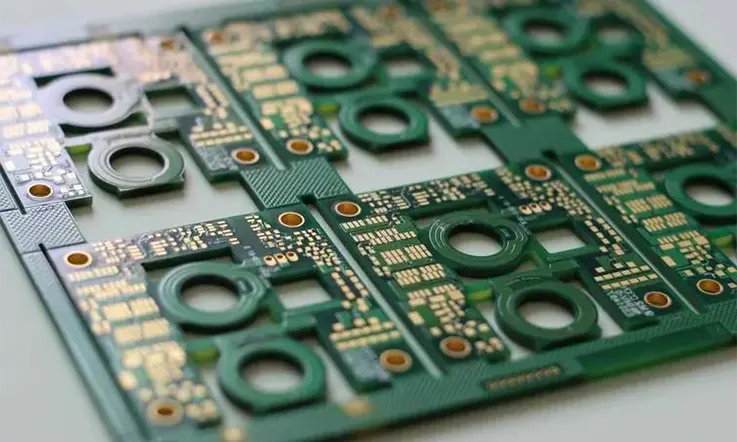
During the manufacturing and assembly processes of circuit boards, there are various potential flaws that can lead to the rejection of boards. These flaws are subjected to testing involving heat excursions, exposure to toxic chemicals, quality inspections, and the use of cleaning agents. However, one flaw that is often overlooked in this procedure is PCB delamination.
Delamination refers to the separation of layers in a laminated board and can occur during assembly under specific conditions related to soldering and material parameters. While it is common for circuit boards to have some degree of delamination in certain areas, extensive delamination must be avoided. This requires careful consideration of materials, reflow profile, pre-bake settings, and laminate storage to ensure proper matching.
The fabrication of circuit boards is a complex process that demands meticulous attention to several factors. PCB delamination is among the potential flaws that can arise, and although preventive measures can be taken, manufacturing errors are often the root cause of this issue. In order to gain a comprehensive understanding of this flaw, it is important to explore its causes, necessary precautions, and available methods for rectification. By delving deeper into this topic, valuable insights can be gained.
What Is PCB Delamination?
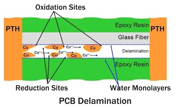
PCB delamination refers to the separation or detachment of layers within a printed circuit board. It is a critical issue that occurs when the bond between different layers of the PCB weakens or fails, resulting in the separation of one or more layers from the rest of the board.
Delamination can occur at various interfaces within the PCB, including between the substrate and copper layers, between copper layers, or even within individual layers. It is typically caused by a combination of factors such as thermal stress, moisture absorption, poor material selection, manufacturing defects, and environmental conditions.
The delamination process often begins with the penetration of moisture or other contaminants into the PCB. Over time, these substances can degrade the adhesive properties of the materials or weaken the interlayer bonds, leading to the separation of layers. Additionally, thermal cycling, where the PCB undergoes repeated heating and cooling, can induce mechanical stress and further contribute to delamination.
PCB delamination can have several negative consequences. It can impair the electrical performance of the board, leading to signal loss, increased resistance, and potential circuit failures. Delamination can also compromise the structural integrity of the PCB, making it more susceptible to physical damage or breakage. In severe cases, delamination can cause complete failure of the PCB and render the electronic device inoperable.
PCB Construction and Layers
PCB (Printed Circuit Board) construction involves the layering of different materials to create a functional circuit board. The number and arrangement of layers depend on the complexity of the circuit design. Here are the commonly used layers in PCB construction:
Signal Layer
The signal layer, also known as the copper layer or the conductor layer, contains the traces that carry electrical signals between components. It consists of thin copper foil laminated to the substrate.
Power Plane
Power planes are layers dedicated to providing power and ground connections to the components on the PCB. They are often placed adjacent to the signal layers. Power planes help minimize impedance, provide stable power distribution, and reduce electromagnetic interference (EMI).
Ground Plane
The ground plane is a dedicated layer that provides a low-impedance path for returning currents and acts as a reference for signal integrity. It is usually placed adjacent to the signal and power layers.
Internal Layers
In multilayer PCBs, there can be one or more internal layers between the outer signal layers. These internal layers may contain additional power planes or signal layers, depending on the circuit design requirements.
Soldermask Layer
The soldermask layer is applied over the signal, power, and ground layers. It covers most areas of the PCB, exposing only the pads and vias. The soldermask provides insulation, protects the copper traces from oxidation, and helps prevent solder bridges during assembly.
Silkscreen Layer
The silkscreen layer contains component reference designators, symbols, logos, and other markings printed on the PCB surface. It assists in component placement, assembly, and identification.
Surface Finish Layer
The surface finish layer is a coating applied to exposed copper surfaces to protect them from oxidation and facilitate soldering during assembly. Common surface finishes include HASL, ENIG, and OSP.
Substrate/Base Material
The substrate or base material provides structural support for the PCB. It is typically made of a non-conductive material like fiberglass-reinforced epoxy resin (FR-4) or other specialized materials for specific applications.
These layers are stacked and laminated together to create a complete PCB. The specific arrangement and number of layers depend on the complexity of the circuit design, the desired functionality, and the manufacturing capabilities.
Types of PCB Delamination
There are several types of PCB delamination that can occur. Here are some common types:
Interfacial Delamination: Interfacial delamination refers to the separation between two adjacent layers of the PCB. It occurs at the interface where the adhesive bonding between the layers fails. This type of delamination can be caused by factors such as poor lamination conditions, inadequate pressure or temperature during manufacturing, or the use of incompatible materials.
Intra-layer Delamination: Intra-layer delamination occurs within a single layer of the PCB. It is characterized by the separation between the copper traces or between the copper and the substrate material within the same layer. Inadequate material adhesion, exposure to moisture, or thermal stress can contribute to intra-layer delamination.
Surface Delamination: Surface delamination refers to the separation between the outermost layer of the PCB and the underlying layers. It is typically observed as blistering, lifting, or bubbling on the PCB surface. Surface delamination can be caused by factors such as moisture absorption, poor material adhesion, or exposure to harsh environmental conditions.
Internal Delamination: Internal delamination occurs within the inner layers of the PCB, away from the outer surfaces. It is often challenging to detect and diagnose internal delamination without destructive testing methods. Internal delamination can be caused by factors such as poor manufacturing processes, inadequate curing of resin, or the use of low-quality materials.
Microscopic Delamination: Microscopic delamination refers to very small-scale separations or voids within the PCB layers that are not visible to the naked eye. These delaminations can be caused by factors such as manufacturing defects, improper material handling, or poor quality control.
It’s important to note that these types of delamination can occur individually or in combination, depending on the specific circumstances and underlying causes. Delamination can significantly impact the performance, reliability, and lifespan of the PCB, so it is crucial to address and mitigate the causes to ensure the integrity of the circuit board.
Causes of PCB Delamination
PCB delamination can occur due to various factors. Here are some common causes of PCB delamination:
Thermal Stress: Excessive heat or thermal cycling can cause differential expansion and contraction of the PCB and its components, leading to delamination. Thermal stress can weaken the adhesive bonds between the layers of the PCB.
Moisture Absorption and Humidity: PCBs are susceptible to moisture absorption, especially if they are not adequately protected. Moisture can penetrate the PCB, causing swelling and delamination. High humidity environments can also contribute to delamination over time.
Poor Material Selection or Quality: The choice of materials used in the PCB manufacturing process is crucial. If low-quality materials or incompatible materials are used, it can result in poor adhesion and increased delamination risk.
Manufacturing Defects and Processes: Defects introduced during the PCB manufacturing process can lead to delamination. Issues such as improper curing of resin, inadequate cleaning, improper lamination conditions, or insufficient pressure during lamination can all contribute to delamination.
Environmental Factors and Contamination: Exposure to harsh environmental conditions, such as extreme temperatures, chemicals, or pollutants, can degrade the PCB’s integrity and cause delamination. Contaminants, such as oils, solvents, or residues, can interfere with the adhesive properties and lead to delamination.
Mechanical Stress: Mechanical stress during handling, assembly, or operation of the PCB can result in delamination. Excessive bending, flexing, or vibration can weaken the adhesive bonds between layers and cause separation.
Age and Degradation: Over time, PCBs can experience aging and degradation of the materials used. This can lead to a loss of adhesion between layers and increased delamination risk, especially in older or poorly maintained PCBs.
It’s important to note that multiple factors can interact and contribute to delamination. Understanding these causes can help in designing and manufacturing PCBs with better resistance to delamination and implementing preventive measures.
What are the Differences Between Measling and PCB Delamination?
Measling is an additional potential issue that can arise alongside delamination, presenting similar symptoms and posing challenges in their differentiation. Nonetheless, they stem from distinct root causes and indicate various manufacturing problems.
Similar to delamination, measling pertains to complications associated with the lamination process. During PCB lamination, insufficient resin application can result in the formation of white spots within the weave of the circuit board, commonly referred to as “measles.”
Delamination, on the other hand, manifests as elevated blisters in the base materials of the circuit board, primarily caused by moisture accumulation. Measling, characterized by white dots, is distinct from delamination. The main typical causes of measling are the inadequate application of resin during manufacturing or high stress at any stage in the circuit board’s life cycle.
Delamination often impairs the performance of the board, whereas measling typically does not have a significant impact, especially in small quantities. As long as the measling does not bridge soldering eyes or conductors, the PCB can generally operate normally.
Measling is likely to occur at some point during the lifespan of the board, but it doesn’t usually raise alarm. However, it is crucial for manufacturers to implement appropriate resin-application processes during production to ensure the circuit board is constructed without measling. While measling may occur later in the board’s life, preventive measures during manufacturing are necessary to minimize its occurrence.
How Can You Determine if a PCB is Damaged or Experiencing Delamination?
To determine whether a printed circuit board (PCB) is damaged or experiencing delamination, you can perform the following checks:
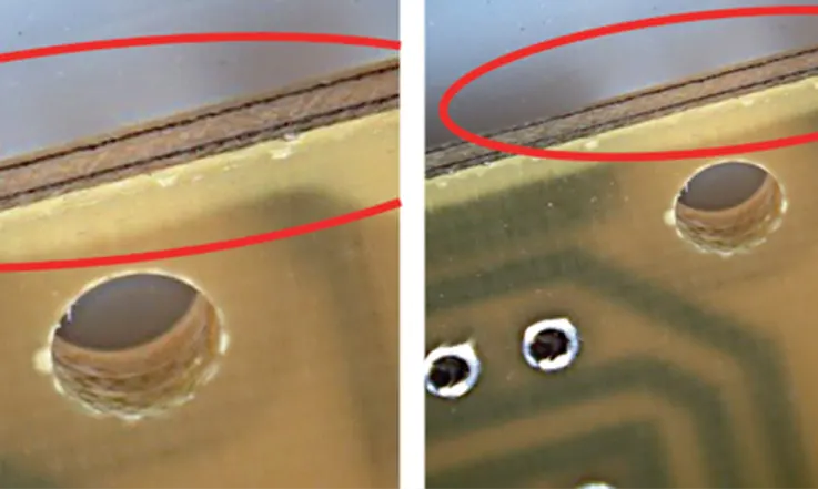
Visual Inspection: Examine the PCB for any visible signs of damage, such as cracks, discoloration, or warping. Look for any areas where the layers of the board appear to be separating or lifting.
Electrical Testing: Use a multimeter or other testing equipment to check the continuity and resistance of the PCB’s traces, pads, and vias. If there are any open circuits or abnormal resistance readings, it could indicate damage or delamination.
X-ray Inspection: X-ray inspection can reveal hidden faults within the PCB, including delamination. X-ray imaging can identify air gaps between layers or variations in material density, indicating potential delamination issues.
Thermal Imaging: Thermal imaging cameras can detect temperature variations on the PCB’s surface. Delamination may cause localized hotspots or thermal irregularities due to poor heat dissipation.
Acoustic Testing: Specialized equipment can detect changes in acoustic properties that may occur when the layers of a PCB separate or delaminate. This method is particularly useful for identifying delamination in high-frequency or microwave PCBs.
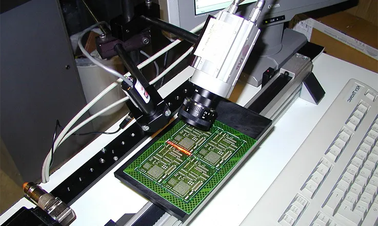
Microscopic Examination: Using a microscope, inspect the PCB for signs of delamination, such as lifted traces or separation between layers. Delamination may appear as visible gaps or cracks under magnification.
Mechanical Testing: Perform a bend test or a flex test on the PCB to assess its structural integrity. Applying controlled mechanical stress can help identify delamination or weak areas that may lead to failure.
It’s worth noting that some of these tests may require specialized equipment or expertise. If you are uncertain about performing these assessments yourself, consider consulting with a professional PCB technician or engineer who can provide a more accurate evaluation.
Tests that Measure PCB Delamination
Detecting defects in a circuit board, particularly delamination, can be challenging as it often occurs internally and remains invisible until visible signs, such as blisters, appear, indicating that the functionality may already be compromised.
The prevention and testing of delamination primarily take place during the manufacturing process. Various testing methods are employed to assess PCB delamination and identify potential issues with the base materials.
One commonly used test is the time test, which measures the duration required for the resin to detach from the copper or reinforcement. In this test, the board is subjected to a specific temperature, and the time it takes for delamination to occur is recorded.
Typical temperature ranges for this test fall between 260° to 288° Celsius, with the 260° test generally considered more precise. It is important to note that the Tg (glass transition temperature) rating of the FR-4 material used in the board also plays a role. Higher Tg values in FR-4 result in quicker delamination compared to lower Tg values.
By implementing these testing methods and considering the Tg rating of the materials, manufacturers can identify and address potential delamination issues during the manufacturing process, ensuring the production of high-quality circuit boards.
Effects and Consequences of PCB Delamination
Delamination in a PCB (Printed Circuit Board) can have various effects and consequences, which can impact the performance, reliability, and functionality of the circuit board. Here are some common effects and consequences of delamination:
Electrical Performance Issues: Delamination can disrupt the electrical connectivity within the PCB, leading to signal integrity problems. It can cause impedance variations, signal reflections, increased noise, and cross-talk between traces. These electrical performance issues can result in data corruption, signal degradation, and ultimately affect the overall functionality of the PCB.
Increased Failure Rates: Delamination weakens the structural integrity of the PCB, making it more prone to mechanical stress and vibration. This can lead to an increased rate of component failures, especially for components that rely on strong mechanical bonds with the PCB, such as surface-mounted devices (SMDs) or connectors. The compromised structural integrity can also make the PCB more susceptible to physical damage during handling or operation.
Reduced Reliability and Lifespan: Delamination compromises the overall reliability of the PCB. It can lead to premature failure, intermittent connectivity issues, and reduced lifespan of the circuit board. The presence of moisture or contaminants within the delaminated regions can accelerate the degradation of other components and materials, further impacting the reliability and longevity of the PCB.
Heat Dissipation Problems: Delamination can hinder the efficient dissipation of heat generated by active components on the PCB. The presence of air gaps or poor thermal conductivity within delaminated regions can create thermal resistance, leading to localized hotspots and thermal stress on components. This can result in thermal failures, thermal runaway, or reduced performance of heat-sensitive components.
Difficulties in Repair and Rework: Delamination can complicate repair and rework processes. The presence of delamination can make it challenging to establish reliable solder joints or establish proper electrical connections during repairs. It may require additional steps, such as removing and replacing delaminated portions or performing intricate rework procedures.
Increased Manufacturing Costs: Delamination issues detected during or after the manufacturing process can result in increased costs. It may require reworking or scrapping of faulty PCBs, leading to material wastage and additional labor and resources. Delamination-related failures in fielded PCBs may also lead to warranty claims, customer dissatisfaction, and additional expenses for product recalls or replacements.
Impaired Testing and Troubleshooting: Delamination can interfere with the effectiveness of testing and troubleshooting processes. Intermittent connectivity issues caused by delamination can make it difficult to identify the root cause of failures or diagnose the exact location of the problem. This can result in increased testing time, delays in identifying faults, and extended downtime for the PCB.
Addressing delamination issues requires preventive measures during design, careful material selection, proper manufacturing processes, and regular inspection and maintenance. Detecting and mitigating delamination early on can help preserve the integrity and reliability of the PCB while avoiding costly consequences.
Preventive Measures and Mitigation Techniques
To prevent PCB (Printed Circuit Board) delamination and mitigate the risks associated with it, here are some preventive measures and mitigation techniques:
Design Considerations
● Optimize PCB layout: Ensure proper trace routing, avoid sharp angles, and minimize the use of long, narrow traces that may be prone to stress.
● Use proper spacing: Maintain sufficient spacing between traces and pads to minimize the risk of electrical breakdown or thermal stress.
● Consider thermal management: Incorporate thermal relief pads, thermal vias, and heat sinks to manage temperature differentials and minimize thermal stress on the PCB.
● Follow design guidelines: Adhere to industry standards and guidelines for PCB design, such as those provided by IPC (Association Connecting Electronics Industries).
Material Selection and Qualification
● Choose suitable substrate materials: Select high-quality materials with good dimensional stability, thermal resistance, and moisture resistance, such as FR-4 or specialized materials for specific applications.
● Verify material properties: Conduct thorough material qualification tests to ensure they meet the required specifications, including thermal cycling, moisture absorption, and mechanical strength tests.
Manufacturing Process Optimization
● Control the lamination process: Maintain proper temperature, pressure, and time during the lamination process to ensure adequate bonding between layers.
● Implement proper surface preparation: Ensure that the surface of the PCB is clean and free from contaminants before lamination to promote good adhesion.
● Optimize soldering processes: Use appropriate soldering techniques and profiles to prevent excessive heat exposure and thermal stress during assembly.
Inspection and Quality Control Methods
● Implement comprehensive quality control measures: Perform visual inspections, automated optical inspections (AOI), and other quality control tests at various stages of the manufacturing process to identify potential delamination issues.
● Conduct reliability testing: Subject the PCBs to environmental stress testing, such as thermal cycling, humidity testing, and vibration testing, to evaluate their performance and durability.
Failure Analysis and Corrective Actions
● Perform failure analysis: Investigate any instances of PCB delamination through failure analysis techniques to identify the root causes and take appropriate corrective actions.
● Improve process documentation: Document the lessons learned from failure analysis and implement process improvements to prevent future delamination issues.
It is important to note that specific preventive measures and mitigation techniques may vary depending on the specific application, PCB design complexity, and environmental factors. Consulting industry standards, guidelines, and engaging with experienced PCB manufacturers can provide valuable insights for effective delamination prevention and mitigation.
What Are the Reasons for PCB Delamination during the Reflow Soldering Process?
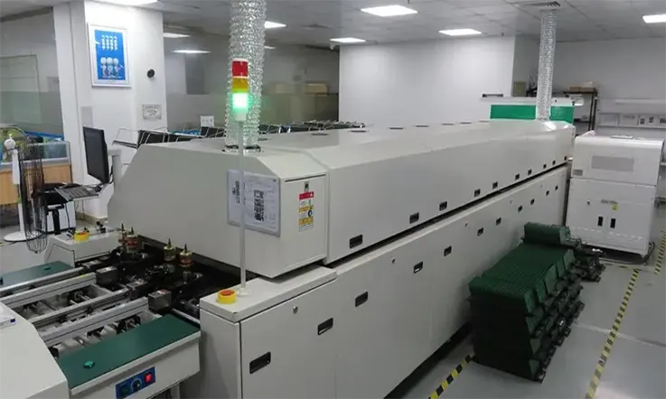
One of the primary causes of delamination in FR4 PCBs during reflow soldering is the presence of moisture within the FR4 material, resulting in swelling and subsequent separation of internal layers.
It is crucial to ensure the appropriate material grade is selected, along with the correct specifications for the intended assembly process.
While moisture can lead to delamination in FR4 PCBs, it is often a consequence of flaws introduced during the PCB manufacturing process.
Given the hygroscopic nature of FR4 material, it is recommended to vacuum seal the PCBs after fabrication. In cases where there are concerns about the sealing process, pre-baking the PCBs to eliminate moisture prior to assembly is advised, following the guidelines outlined in IPC 1601.
Summary
Addressing PCB delamination requires a comprehensive approach involving design, materials, manufacturing processes, inspection, and failure analysis. Further research and development efforts in this field are essential to enhance the understanding of delamination mechanisms and to develop more advanced techniques for prevention and detection.
By implementing the knowledge gained from studying PCB delamination, engineers and PCB manufacturers can improve the reliability and performance of electronic devices, ensuring the long-term functionality and durability of PCBs in various applications.
Related Posts:
1. What Is PCB Etching and How to Make a perfect PCB Etching?
2. The Best PCB Panelization Guide
3. The Importance of 3D Printed PCBs in Modern Electronics Production
5. The Best Backplane Printed Circuit Boards Factory
6. An Overview of Through-hole Technology (THT)
7. Detail Talk Surface Mount Technology