The drilling process is the most time-consuming and labor-intensive step in the fabrication of boards.The process of drilling PCBs needs to be carried out with extreme caution because the slightest mistake might result in a significant financial loss.It is generally agreed that the drilling process is the most important and time-consuming part of the fabrication of printed circuit boards.Before making an order, a PCB design engineer has the responsibility of always investigating the capabilities of the PCB board manufacturer.
The drilling procedure lays the groundwork for vias, which are used to establish communication between the various layers. The move away from stationary to portable technology was precipitated by the miniaturization of electronic equipment such as televisions and mobile phones. To achieve the desired reduction in size, high-quality micromachining is required.The process of drilling is critical to making this possibility a reality. Therefore, the drill technology that is utilized is important.
What Is Printed Circuit Boards Drilling?
The process of making holes, slots, and many other cavities in an electrical circuit board is referred to as “PCB drilling,” which is also another name for printed circuit board drilling.
During the drilling process for PCBs, holes of a variety of configurations and sizes are drilled. These are known as via holes, component holes, and mechanical holes. Other names for these types of holes are thru-holes, buried holes, blind holes, and micro-holes.
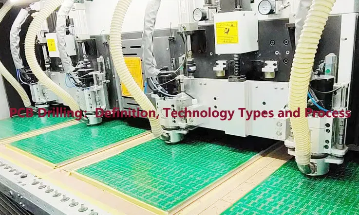
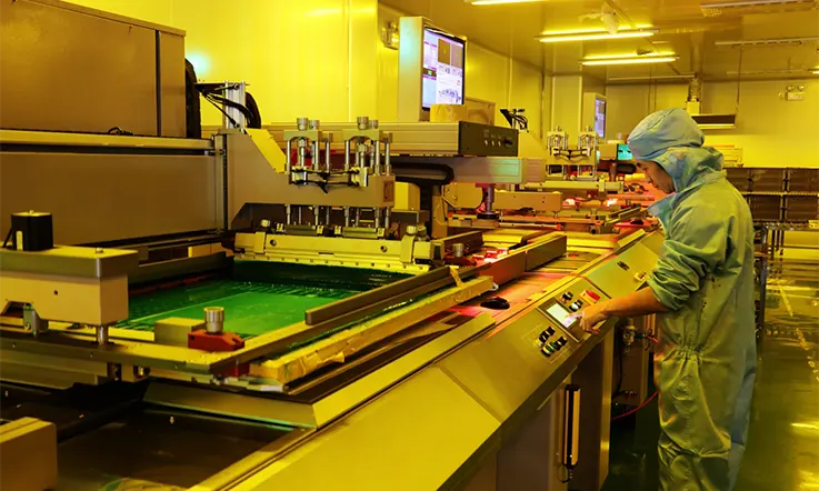
In order to achieve the desired level of precision, holes are often drilled into a PCB using either a manual or laser PCB drill. A manual process or an automated one can be used to feed boards into a drilling rig. At JarnisTech, we have a drill that has a function that can detect lasers. Even when it is not manned, this guarantees that the concentricity and accurate bit diameter (0.1mm-6.5mm) are maintained.
Types of PCB Drilling
● Circuit Drill Bit: The drill that is known as a circuit board drill bit has one end that is shaped like a point and the other as a flat surface. Its primary function is to make holes in various materials, typically for the purpose of inserting and welding wires. Make sure that the face that is flat is facing the surface at all times so that it does not move in any other direction. This will help you achieve a better result. In the end, it produces a hole in the circuit board of the printer that is at a straight angle.
● A Back Drill: The creation of holes in PCBs typically requires the use of a tool called a back drill PCB. However, these holes are further utilized for the hand-insertion of wires in the majority of cases. After that, the surface of the PCB is cut with a sharp blade, which exposes the copper layer underneath it. Burr cutters are used to remove this layer of copper from the circuit board. After going through this procedure, a back-drill PCB will be able to function electrically while still being linked to its main power supply circuit board.
● PCB Hand Drill: To engrave holes into the PCB, a hand drill designed specifically for use with printer circuit boards (PCB) is required. The PCB hand drill features a chunk that is attached to it and serves the purpose of ensuring the drill does not move while in use. This chuck can be tightened with either an Allen key or a wrench depending on your preference. This drill comes with its very own specific instructions regarding the contents of the packaging and how it should be used.
Drill Technology In PCB Manufacturing Process
Mechanical drilling and laser drilling are the two primary categories of drilling technologies available today.
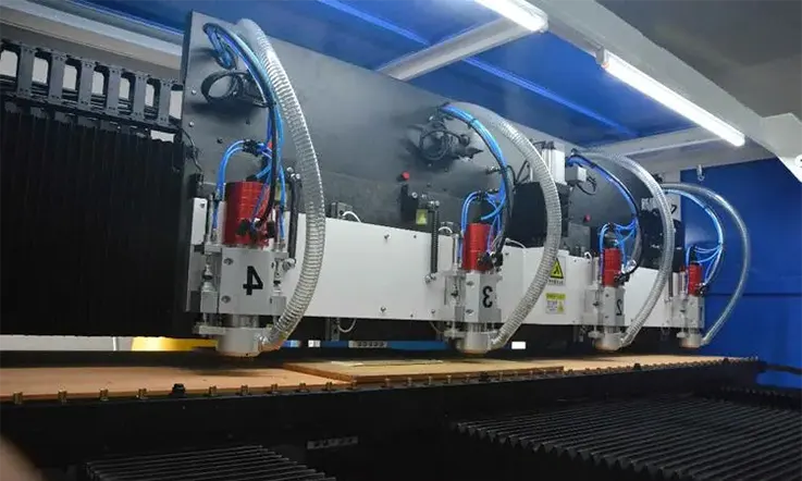
Mechanical Drilling
The mechanical drills offer a lower level of precision but are much simpler to operate.Drill bits are an important component of this drilling technology. These drills have a capability of drilling holes with a diameter of approximately 6 mils (0.060″) at their smallest setting.
Mechanical Drill Limitations: When working with softer materials like FR4, mechanical drills have a maximum capacity of 800 strikes.When dealing with denser material like as Rogers, the lifespan is cut down to 200 counts. If a PCB manufacturer ignores this, then it will lead to faulty holes, which will result in the board being rendered useless and scrapped.
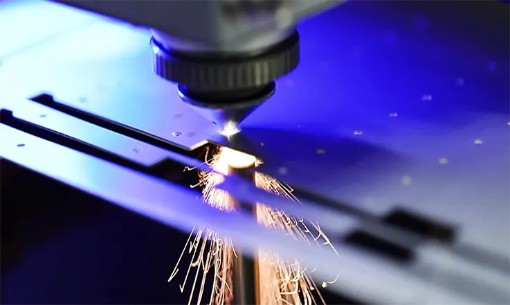
Laser Drilling
On the other hand, laser drills are able to create holes that are much more minute. Laser drilling is a non-contact procedure, which means that the work piece and the tool do not come into touch with each other at any point during the operation.A laser beam is used to remove material from the board and make holes with a high degree of accuracy. Here, the depth of the drill can be easily adjusted as needed.
In order to drill regulated depth vias more easily, the technology of laser drilling is utilized. Precision drilling down to a minimum hole diameter of two mils (0.002 inches) is possible here.
Laser Drilling Limitations: Copper, glass fiber, and resin are the three basic components of a circuit board.The PCB materials in question each have their own unique optical characteristics. Because of this, it is more difficult for the laser beam to effectively cut through the board. When it comes to the expense of the process, laser drilling is typically among the more expensive options.
It is beneficial for the designer to have some familiarity with the activities that take place on the shop floor so that they can acquire a better understanding of how the design is brought to life. The designer of the circuit board uses this information to ensure that the designs can be manufactured successfully.This, in turn, brings about a reduction in costs, and it also makes it possible for the product to be delivered in the shortest possible amount of time.
PCB Drilling Process: 4 Steps
For each layer’s circuit to be connected, the boards must be drilled according to the specifications in the drill files to create the corresponding holes. Single- and double-sided boards are pierced immediately after cutting, whereas multi-layered boards are drilled following lamination. And the PCB drilling procedure can generally be broken down into four steps:
1.Drilling Location Holes:During the production and testing operations of a printed circuit board (PCB), the location holes function as the positioning points. Before beginning the drilling process, the backing board, the substrate, and the aluminum sheet are first placed on the table of the high-speed drilling machine in the reverse order of how they were removed. On the border of the circuit board, three to four placement holes of approximately 3.2 millimeters in diameter are drilled in accordance with the instructions for production.
2.Inserting Pins:In order to maximize the effectiveness of the production process, multiple boards are stacked before being drilled. To prevent shifting and dislocation, however, these boards must first be taped onto the table of the drilling machine through the pins while simultaneously holding the backing board and the covering plate together.
3.Drilling Holes:Since the drilling process is managed by a computer program, all that is necessary to drill the appropriate holes is to input the CAM-converted drilling parameter files. In the process of fabricating printed circuit boards (PCBs), mechanical drilling is a technology that is frequently employed to drill holes. When drilling a variety of different sorts of holes, such as Plated Through Holes (PTH), Non-Plated Through Holes (NPTH), and Via Holes, the drill bit is rotated at a high speed through the spindle, which generates a cutting force and allows for the creation of a number of different types of holes. A backing board is placed underneath the board before drilling begins to protect the surface of the drilling machine. Additionally, a sheet of aluminum is set on top of the backing board to make the holes in the copper foil flatter and to prevent the bit from overheating.
4.Hole Inspection: After the hole has been drilled, the aperture and placement of the hole on the first sample of the board should be examined. After ensuring that there are no issues such as additional holes, missing holes, or hole shift, then it is ready to move on to the subsequent stage of the manufacturing process.
Considerations in the PCB Drilling Process
During the drilling process, it is essential to keep in mind the following two factors:
Drill to PCB Copper Clearance
The drill to copper distance refers to the amount of space or land clearance that exists between the edge of a drilled hole and the nearest copper feature.
Having said that, the copper feature that is the closest to you might be an active copper region or a copper trace. Because even a tiny variation might throw the circuit off, this variable plays a vital part in the drilling process.
In addition, the standard value of the drill to copper is approximately 0.008 inches (or eight mils).
Note:
Minimum clearance = width of annular ring + solder dam clearance.
Aspect Ratio
The aspect ratio is determined by how effectively the holes plate copper and how well they plate copper. When the diameter of the hole is decreased while the depth of the hole is increased, it is without a doubt quite difficult to copper plate the inside part of the hole.
In this case, you will need to carry out a plating bath in order to solve the problem. And while you’re at it, try increasing the force behind your throws. As a direct result of this, the liquid will work its way through the extremely small holes.
In light of the aforementioned, the aspect ratio of microvias is 0.75:1, but the ratio of through-holes is 10:1. Additionally, the smallest drill size that may be used on a PCB with a thickness of 62 mil is six miles.
Note:
AR (Aspect Ratio) = hole’s depth/ diameter of your drilled hole
Different Holes Drilled in a PCB
A bare circuit board will have a number of constructed properties, such as cutouts, slots, and the general shape of the finished product. The holes that were bored into the board account for the greatest number of these features. The function of these holes can be broken down into three categories, which are as follows:
1.Mechanical Holes
A printed circuit board (PCB) will typically have mechanized components such as brackets, connectors, and fans attached to it. In order to mount these things, holes are required in them. If the object to be installed requires an electrical connection to the PCB, such as a chassis ground, then the holes in the PCB may be plated with metal. However, this occurs only infrequently.
Mounting holes can, in certain circumstances, be utilized as a means of conducting heat away from hot interior layers. The production of printed circuit boards (PCBs) can also be made more efficient by using them. Some people refer to mechanical holes as “tooling holes,” particularly when they are utilized to match a printed circuit board (PCB) to an automated manufacturing machine.
2. Component Holes
Despite the fact that surface mount components are used for largely passive and discrete PCB components, the majority of them may nevertheless integrate well with through-hole packages. Connectors, switches, and other mechanical components that call for a sturdy mounting solution that is ensured by a through-hole packaging are included in this category of components. In addition, because of their ability to transmit both current and heat, these packages are an excellent choice for power components such as large resistors, capacitors, operational amplifiers, and voltage regulators.
3. Via Holes
Electrical signals, power, and ground can be transmitted across the PCB layers using tiny metal-plated holes. Vias are the name for these holes, and there are several sorts depending on the needs.
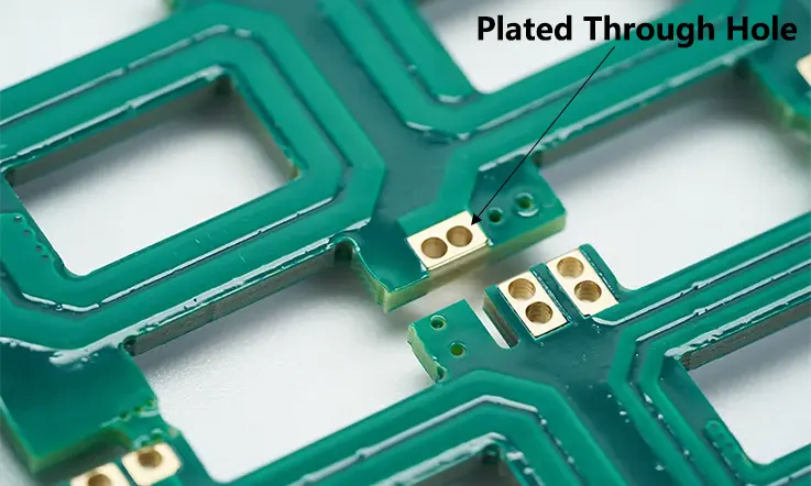
Through-hole: A through-hole is a type of standard via that runs all the way from the top of the board to the bottom of the board. These vias connect various traces or planes to the many different layers.
Micro: Laser machines are used to make micro vias, therefore their holes are much smaller than those found in other types. As a result of the difficulties associated in plating smaller holes, they often consist of two layers. Micro vias are a good choice for HDI boards or other devices with a large pin count and fine pitch, such as BGAs.
Blind: These vias begin in the surface layers but only penetrate midway through the board. Earlier, we mentioned that creating blind vias is costly, but they provide sufficient capacity for routing. The signal quality of high-speed communication lines can be improved by their shortened barrel.
Buried: A buried via is a via that is entirely contained inside the inner layers of the PCB and does not extend to any of the surface layers. They take up less room than through-hole vias do, which makes them acceptable for use on high-density interconnect (HDI) circuit boards. Nevertheless, the creation of buried vias might be quite pricey.
Tips and Tricks
● Add solder to drilled holes.
● Clean your PCB after drilling.
● Use a drill press for precise drilling holes.
● Start with pilot holes for appropriate drilling.
● Address any close gap that is less than six miles.
● Ensure that your non-plated drills have a connection.
● Confirm that you have a defined drill type (NPTH/ PTH).
● Ensure that your aspect ratio is low to prevent drill wear.
● When you’re drilling at an angle, use only a straight PCB drill.
● Verify your size or drill count between the drill file and Fab print.
How Can You Get Started with JarnisTech?
More than two decades ago, we at JarnisTech began providing a PCB fabrication service that was at the cutting edge of its day. We have perfected our procedures to ensure that we are able to provide PCB goods of the best possible quality in the shortest amount of time.
Because of our extensive experience, we are able to provide a comprehensive selection of PCB services that can be tailored to satisfy specific demands regarding design, manufacturing, and assembly. Please do not be hesitant to get in touch with us if you are unsure exactly what it is that you require or if you would want to discuss this matter with a member of our staff. You can get in touch with us by sending an email to [email protected], calling us at 0086-755-23034656, or filling out our contact form.
Summary
In recent years, there has been an emphasis placed on optimizing the drilling process in comparison to older technologies. The precision of the drills is getting extremely close to being perfect as a result of the exponential growth that has occurred in the circuit board business. We are confident that you now have a clearer understanding of how the PCB drilling procedure is carried out.It seems to be very challenging, doesn’t it? Don’t freak out.Simply send over your design files in Cerber format to JarnisTech. Allow us to perform the task at hand while you kick back, watch Netflix, and relax.
Related Posts:
- An Overview PCB Laser Drilling
- PCB Mechanical Drilling
- What Is PCB Etching and How to Make a perfect PCB Etching?
- The Best PCB Panelization Guide
- The Importance of 3D Printed PCBs in Modern Electronics Production
- Understanding PCB Delamination: A Comprehensive Guide
- The Best Backplane Printed Circuit Boards Factory
- An Overview of Through-hole Technology (THT)
- Detail Talk Surface Mount Technology
- PCB Clone : Copy Your Printed Circuit Board
- Rigid PCB Capability