To establish connectivity between different layers in Printed Circuit Boards (PCBs), holes need to be drilled through or partially drilled in the laminate. These holes serve to connect the traces and pads of different layers. However, the process of drilling is costly and time-consuming in PCB manufacturing because even a slight error can lead to significant losses. Therefore, two technologies, mechanical drilling and laser drilling, are used to drill holes in the PCB manufacturing process.
In this artcle, we will dicuss definition of Mechanical drilling, advantage, disavantage, important in the PCB fabrication and And the difference between it and laser drilling. Now, lets go.
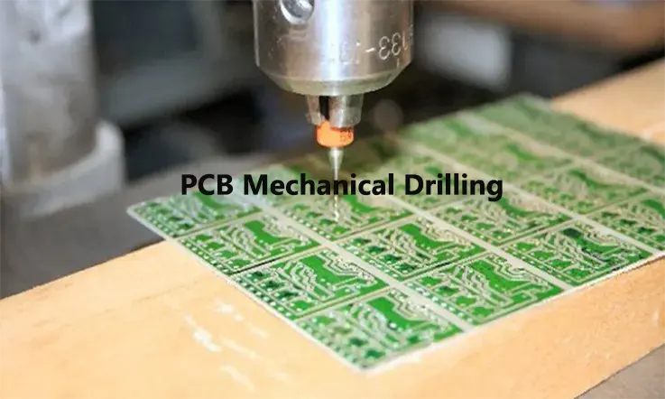
What Is PCB Mechanical Drilling ?
PCB mechanical drilling is a process in which small holes are drilled into printed circuit boards (PCBs) using a mechanical drill. The drill makes contact with the surface of the PCB, and rotates at a high speed to produce a hole with the desired diameter and depth. This process is a critical step in PCB fabrication as it creates holes for the insertion of electronic components, such as leads and pins, allowing them to be soldered onto the PCB. The process can be performed manually or with computer-controlled (CNC) machinery.
When mechanically drilling holes in a PCB, manufacturers rely on a rotating bit tool. These bit tools have a special design making them capable of cutting through various types of laminate materials. Bit tools are available in many sizes defining their diameter, and made from hardened carbide steel material. As a standard PCB consists of glass fiber and resin, and has a copper foil covering on top, it is a tough material for the bit to cut through. The hard material prevents the bit from wearing out fast and allows it to cut many holes before needing a sharpening.
Advantages of Mechanical Drilling
● One of the key benefits of utilizing drill bits for mechanical drilling in PCB manufacturing is the ability to produce high-quality holes consistently, regardless of the number required. The drill bit facilitates the creation of holes with uniform diameter, devoid of any tapering, knees or bevels, even when passing through multiple substrates. Furthermore, the surface of these holes maintains a sharp finish, meeting the stringent design requirements.
● Compared to other drilling methods, mechanical drilling stands out for its efficiency, speed, and consistent performance levels, making it a preferred choice for high-throughput PCB manufacturing. Manufacturers can rely on mechanical drilling to create large numbers of high-quality holes, reducing the risks of errors, defects, or damage to the material.
● In addition, mechanical drilling is a critical technology in PCB manufacturing, delivering high-quality output, consistent results, and fast production cycles. The versatility and reliability of this method also contribute to the production of superior PCBs, ensuring that manufacturers meet their customers’ demands for quality and performance.
Disadvantages of Mechanical Drilling
● Mechanical drilling is an effective method for PCB production, but it has several drawbacks that manufacturers must consider. One significant limitation is the size of the drill bit, which can easily break when drilling narrow holes through multiple layers of material. This is especially true for high-density PCBs with small via holes, which require tiny drill bits that increase the risk of breakage.
● Another challenge of the mechanical drilling process is the formation of elevated copper ends after drilling holes, which requires additional deburring steps to remove. Depending on the number of holes drilled, deburring can be time-consuming and add to the cost.
● Mechanical drilling is an expensive process, and several pre- and post-processing steps are necessary to achieve quality results. Proper tool selection, drill bit preparation, and setup are essential for efficient and effective drilling. However, when multiple diameter holes are required, the process can become time-consuming, particularly if performed manually, increasing the chance of errors and creating more waste.
● To mitigate these challenges, manufacturers must carefully match the drilling method to the PCB design and production process, and equip themselves with suitable handling, equipment, and processing practices to reduce the drawbacks’ impact. By doing so, they can ensure a reliable and efficient production cycle that meets their customers’ demands for quality and performance.
PCB Layout Considerations for Mechanical Drilling
Here are some PCB layout considerations for mechanical drilling:
● Hole-to-edge clearance: There needs to be enough clearance between the drilled hole and the edge of the PCB to avoid any potential damage to the board or drilling equipment.
● Hole alignment: The holes to be drilled should be accurately positioned on the PCB layout to ensure that they are in the correct location with respect to the other circuit components.
● Drill hole size: The hole sizes for mechanical drilling should be chosen based on the size of the components that will be mounted on the PCB and the specific tolerances required for each hole.
● Hole density: The spacing between holes should be sufficient to allow for proper alignment, but also optimized to minimize the number of holes and reduce the drilling time for manufacturing.
● Hole aspect ratio: The ratio between the hole diameter and the board thickness, also known as the aspect ratio, should be kept at appropriate levels to ensure that the holes are mechanically and dimensionally stable.
● Drill breakage and damage prediction: In addition to designing the drill holes, it is also important to consider the possibility of drill breakage or damage, which can be predicted using analysis or simulation tools to redesign the board accordingly.
● PCB material: The type and thickness of material used for the PCB can affect the choice of drill bit or drill machine, as well as impact the accuracy and quality of the drilled holes.
By taking into account these considerations during the PCB layout process, manufacturers can optimize the design for mechanical drilling and ensure that the final product adheres to the required standards for quality and accuracy.
Drilling Techniques and Practices
Here are some common drilling techniques and practices used for PCB mechanical drilling:
● Peck drilling: This technique is used for drilling deeper holes and involves retracting the drill bit periodically to remove any chips and to allow coolant into the hole for lubrication.
● Back drilling: This technique involves drilling holes from the back of the board to partially remove conductive layers or isolation to avoid transmission of signals to unwanted layers.
● Step drilling: This technique involves drilling holes in multiple steps using progressively larger drill bits, which allows for precise control of the hole diameter and depth, particularly for deeper holes where full depth drilling can cause inaccurate results.
● Controlled-depth drilling: This method uses equipment that is able to accurately set and control the drilling depth, which is particularly useful for drilling on multilayer PCBs, as it can prevent damage to inner circuitry.
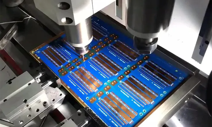
● Automatic tool change: With the use of a CNC drilling machine, automatic tool change can be facilitated, which minimizes changeover time, allowing for efficient drilling and higher productivity.
● High-precision micro-drilling: This practice uses specialized equipment and high-quality diamond-coated drills for the drilling of extremely small holes with diameters that range between 0.1 mm and 0.5mm.
By using these techniques and practices, manufacturers can achieve greater accuracy and speed, reduce tool wear, and improve the overall productivity of the drilling process in PCB fabrication.
Importance of Mechanical Drilling in PCB Fabrication
Mechanical drilling is an essential process in the fabrication of printed circuit boards (PCBs). Here are some reasons why:
● Required for Component Placement: Holes drilled during the mechanical drilling step allow electronic components to be mounted and secured onto the PCB. These components may include resistors, capacitors, diodes, ICs, and other electronic devices.
● Precise and Accurate: The mechanical drilling process is highly precise and accurate, allowing for the creation of small and uniform holes. This precision is essential to ensure that the finished board functions properly.
● Versatile: Mechanical drilling can produce holes of varying diameters, depths and shapes, making it a versatile manufacturing capability that meets diverse design requirements of PCB.
● Automation Capability: PCB mechanical drilling can be automated using computer numerical control (CNC) machines, which can drill multiple holes at once and offer consistently high accuracy in a short period of time.
● Cost-effective: Mechanical drilling is a cost-effective means of creating holes on PCBs, as the drill bits are relatively inexpensive and it requires no special material like lasers.
Because of these reasons, PCB mechanical drilling is a vital step in PCB manufacturing that ensures that the finished board meets functional and performance requirements.
Mechanical Drilling Technology vs. Laser Drilling Technology
For continuity to exist between different layers of a printed circuit board (PCB), holes must be drilled through or partially in the laminate to connect the respective traces and pads. Drilling these holes is a crucial and complex step in PCB manufacturing, as small errors can lead to significant losses in time and resources. Two primary technologies used for drilling holes during PCB manufacturing are mechanical drilling and laser drilling.
Mechanical Drilling Technology
Mechanical drilling is a popular method for drilling holes in different types of laminate materials in PCB production. This technology utilizes a rotating drill bit, typically made of micro-granular cemented carbide, that is capable of drilling numerous holes before replacement. The drill bit can also undergo resharpening up to three times.
One of the significant advantages of mechanical drilling is its ability to create high-quality and consistent holes, regardless of the number required. Also, holes drilled using this technology lack taper, and the knee of the wall is blocked without bevels. Additionally, mechanical drilling is faster than other methods, contributing to a higher throughput.
However, after every drilling cycle, deburring is necessary to remove elevated copper ends that may remain. This process can be time-consuming and lead to production delays. Besides, mechanical drilling may not be suitable for microvias due to its limitations. The technology cannot drill holes smaller than 6 mils in diameter, making it unable to achieve the precision depth required for microvias.
Laser Drilling Technology
Laser drilling is a technology used in PCB manufacturing that utilizes high-density laser beams to create microvias. Two commonly used types of lasers used in laser drilling are UV and CO2 lasers. Through beam shaping technology, the laser beam targets the material surface, breaking chemical bonds and generating steam that applies downward force on the remaining molten material, allowing for the flow of molten material out of the hole.
Laser drilling’s primary advantage over mechanical drilling is its ability to ablate various substrate materials using different diameters not obtainable through mechanical drilling. As a non-contact technique, laser drilling requires less processing and tool selection than mechanical drilling, leading to faster processing times and higher throughput.
However, laser drilling also presents several drawbacks. Without a metal stop layer, it is difficult to achieve precise depth control, leading to tapering from large aspect ratios. Additionally, laser drilling can carbonize the cutting edges, resulting in a burnt or black appearance.
When to Use Mechanical Drilling or Laser Drilling ?
Deciding on the drilling method to use when creating holes in a printed circuit board (PCB) primarily depends on the aspect ratio of the holes and the pad-to-hole diameter ratio. The aspect ratio refers to the ratio of hole diameter to its depth, while the pad-to-hole ratio is more critical during the PCB fabrication process than its design phase.
● Through-Hole Vias: A typical via hole diameter is 0.010 inches, with a tolerance of ±0.003 inches, and manufacturers usually place via holes in the center of the conjoining pad. The smallest diameter of the drilled hole and the overall thickness of the board before the plating process determines the aspect ratio, with larger aspect ratios making the plating process more challenging, increasing the plating time, and the likelihood of creating cracks in the hole wall due to expansion.
To reduce the chances of creating cracks in the hole wall, fabricators often use a rule of thumb to employ larger vias for thicker boards. During fabrication, the usual practice for the copper pad of a via hole is to make it 0.015 inches larger than the desired finished size of the hole. For example, a 0.010 inch via hole would need a 0.025-inch copper pad. The manufacturer can drill a via hole with a diameter of 0.015 inches, with final plating and surface finish eventually bringing the hole diameter to 0.010 inches ±0.003 inches.
Consequently, the aspect ratio and pad-to-hole diameter ratio are determinants in selecting the appropriate drilling method for creating holes in a PCB. To enhance the quality of the holes and reduce production costs, fabricators should use larger vias for thicker boards and ensure greater precision in the placement of via holes.
● Buried and Blind Vias: To optimize the design and functionality of multi-layered printed circuit boards (PCBs), fabricators commonly employ buried and blind vias instead of through-hole vias that pass straight through the board. Through-hole vias are usually reserved for simpler two-layered PCBs.
While both mechanical drilling and laser cutting techniques can be used to create buried and blind vias, laser cutting can result in less accurate depth and generate tapering along the hole edges. Fabricators may introduce an etching step to assist the laser with cutting through the substrate, while ensuring that the copper pad beneath is not ablated. Strict adherence to proper procedures and precautions is necessary to achieve the desired manufacturing results for the PCBs.
Common Mechanical Drilling Defects and How to Avoid Them
Here are some common mechanical drilling defects that can occur in PCB fabrication and some ways to avoid them:
● Drilled Hole Breakout: This defect takes place when the drill bit exits at the wrong location or breaks through to an adjacent layer or the board’s edge, and causes unacceptable damage. To avoid this defect, accurate pre-drill alignment and suitable design rules for board contours and drilling have to be considered. Additionally, drill parameters must be carefully fine-tuned to optimize drilling quality and minimize the risk of drill breakout.
● Burr Formation: This defect occurs as a drill exits the board material and creates burrs or protrusions around the hole. Burr formation is influenced by several factors such as the drill’s clearance angle and the hole aspect ratio, which must be controlled to minimize this defect. Proper drill sharpness, chips evacuation, and lubrication can also help to prevent burrs formation.
● Drilled Hole Residue: Residue can occur during drilling due to chip and material fragments getting stuck in the holes. This defect can be avoided by using optimized pecking cycles to remove the waste chips and keeping the drill bit sharp and lubricated.
● Drill Bit Fracture: The drill bit is prone to fracture when it encounters hard or abrasive material, or due to feed rates that exceed the recommended parameters. To prevent drill bit fracture, appropriate drill selection such as using diamond or carbide coated bits with a suitable flute number, adequate cooling and use of compatible drilling parameters are recommended.
● Oversizing/undersizing of holes: This defect takes place when holes exceed or are below the specified size, affecting precise incorporation of components. This defect can be avoided by proper drill tool selection, regular operator calibration of drills and machines, and having drill control mechanisms in place.
By following recommended procedures and guidelines during the manufacturing process, as well as using proper equipment and techniques, these common mechanical drilling defects can be prevented, leading to a higher quality and more reliable final product.
Conclusion
PCB mechanical drilling is a critical process in the fabrication of printed circuit boards. It involves the removal of material through a rotating drill bit to create holes for components and vias that connect different layers of the PCB. Although it is a mature technology, there are still challenges in achieving high precision and quality while minimizing costs and time-to-market.
With the increasing demands for smaller and more complex devices, there is a need for advanced drilling techniques and equipment. PCB manufacturers are exploring the use of lasers, robots, and automation to improve accuracy, consistency, and efficiency. They are also experimenting with new materials and drilling methods to meet the evolving needs of the electronic industry.
However, even with new technologies, mechanical drilling will continue to play a significant role in PCB fabrication. It remains a cost-effective and reliable way to create holes in a wide range of materials and sizes. To optimize the mechanical drilling process, it is essential to understand the various factors that affect it, such as drill bit type, speed, feed rate, and coolant delivery.
Overall, PCB mechanical drilling is a critical process that warrants careful attention and optimization. By staying abreast of the latest developments in drilling technology and understanding the underlying principles, PCB manufacturers can ensure high-quality and reliable products that meet the needs of the electronic industry.
JarnisTech, as a PCB and PCBA manufacturer in China, has been serving the industry for 20 years. We take immense pride in providing high-quality one-stop service to our esteemed clients, from PCB manufacturing to component procurement and full turnkey PCB assembly. Our commitment to excellence has earned us trust and support from clients worldwide.