In today’s world, electronic devices often require higher component and trace densities, and as a result, vias are gradually shrinking while simultaneously increasing in aspect ratio.There are more microvias in multilayer PCB boards because these boards have smaller traces, sometimes as thin as 3 mil (0.075 mm). When it comes to the production of high density interconnects (HDI) for printed circuit boards (PCBs), microvias are an extremely important component. The vast majority of PCB manufacturers are able to drill via holes as small as 6 mil (0.15 mm) in diameter, but mechanical drilling increases tooling costs. This is because the used drills are so thin that they break readily, particularly if your microvias have a high aspect ratio.
It was difficult to drill holes smaller than 6 mil (0.15 mm) in the traditional method of producing printed circuit boards (PCBs). When the technology for laser drilling began to grow more quickly. Traditional mechanical drilling has many restrictions that can be solved using laser drilling. Laser drilling can be used to make microvias in HDI printed circuit board fabrication, and it is not restricted by the same material limits as traditional mechanical drilling.
What Is Circuit Board Drilling?
The term “circuit board drilling” refers to the process of drilling holes on a printed circuit board (PCB) for any of the purposes that are outlined in the following paragraphs.
●Placement of components.
●To bring interconnection between different layers.
These are accomplished through the utilization of a variety of vias, specifically through-hole vias, microvias, blind vias, and buried vias. Blind vias are chosen over through-hole vias for use as electrical interconnections between layers. This is because blind vias are not visible to the naked eye. In comparison to through-hole vias, blind vias result in an increase in the amount of available space for wiring.
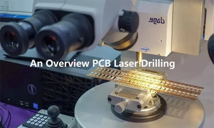
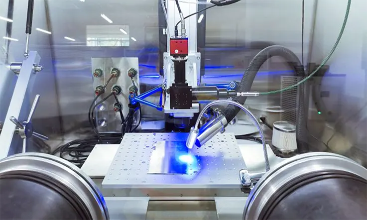
PCB Laser Drilling
Laser drilling, also known as laser ablation, is a process that uses a laser to make precise holes on a printed circuit board (PCB) in order to build connections between various copper layers. The cutting-edge technology that we are all familiar with consists of HDI boards that have laser-drilled microvias integrated into them. Even when working with extremely minute dimensions, the use of laser drilling processes ensures accuracy.
The acronym “laser” refers to “light amplification by stimulated emission of radiation,” which is well knowledge. The process of using highly concentrated laser energy for the purpose of drilling (also known as ablating) a hole is referred to as laser drilling. It is not at all like manually making holes with a drill bit like you would do in a machine.
Consequently, Laser (light amplification by simulated emission of radiation) drilling is a process that utilizes lasers that are highly concentrated to drill hole on PCBs.
Types of Laser Drilling
PCB manufacturers utilize a wide variety of lasers for the drilling of microvias into the boards. There are five laser combination systems that are very well-liked on the market today:
● CO2 Laser
● Yag/CO2 Laser
● CO2/TCO2 Laser
● UV/Tag Laser
● UV/Excimer Laser
Because printed circuit board makers work with a variety of dielectric materials, including resin (either liquid or dry film), reinforced prepreg, and RCC, many laser combinations are required. PCB manufacturers are able to successfully generate dependable microvia holes by using one of the five laser methods described above, in conjunction with the dielectric material being used.
We use CO2 lasers for infrared wavelengths since these lasers are not only affordable but also easily accessible. The CO2 laser is utilized most frequently for the processing of laminates that do not contain glass fibers. Some examples of these laminates are those that are reinforced with aramid fibers, flexible polyimide, and resin-coated copper or RCC foils. We find that the Transversely Excited Atmospheric, or TEA, CO2 laser, which has a higher peak power, is the most effective tool for lazing through glass fibers.
What Are the Methods of PCB Laser Drilling?
● Helical Laser Drilling: When performing helical laser drilling, the laser beam moves along a helical path while rotating about its own axis with respect to the workpiece. This allows the laser to drill holes more precisely. The direction in which the laser beam travels is determined by a dove prism.
● Trepanning: Trepanning is the process of directing a laser beam around a predetermined location. The center of the via to be drilled is at this locus. When the diameter of the via to be cut is greater than the diameter of the laser beam, it is utilized. The mobility of the beam determines how accurate the via is.
● Single-pulse&Shot Laser Drilling: In single-pulse laser drilling, the process of creating the desired hole in the material is accomplished by directing a single laser beam pulse at the target area of the material. Both the source of the laser and the material being worked on remain in their original positions throughout this process.
● Percussion Laser Drilling: The process of percussion drilling involves repeatedly firing a sequence of laser pulses at the material being drilled. During this stage of the process, the laser beam and the workpiece do not move in any relative motion to one another. In comparison to single-shot laser drilling, this method of laser drilling produces holes that are both more precise and deeper, while also having a smaller diameter.
Advantages of Laser Drilling
The following are some of the primary benefits that come with using lasers to drill holes in PCBs:
● Lasers have the ability to ablatively cut through a wide variety of materials.
● Drilling with a laser is an automated process that does not involve the selection of tools by hand.
● Lasers may generate holes with a diameter that is significantly smaller than what is possible with conventional mechanical drill bits.
● When compared to mechanical drilling, laser drilling is capable of producing a significantly greater number of holes in the same amount of time.
● Multi-Tasking: Laser machines can also be utilized for weld and cut operations.
● No drilling vibration: Since laser drilling is a non-contact procedure, there is no drilling vibration that results from using laser drilling. In addition, the material is not harmed in any way by the process.
● High Aspect Ratio: Providing a high aspect ratio is feasible when using laser drilling as the cutting method. It is well knowledge that a typical microvia will have an aspect ratio of 0.75:1.
● Accuracy: When using a laser for drilling, one of the most significant benefits is that one is able to exert complete control over the beam’s strength, as well as the amount of heat produced and the amount of time that the laser beam is active. That it means precision and accuracy in the kind of holes, is a given!
Disadvantages of Laser Drilling
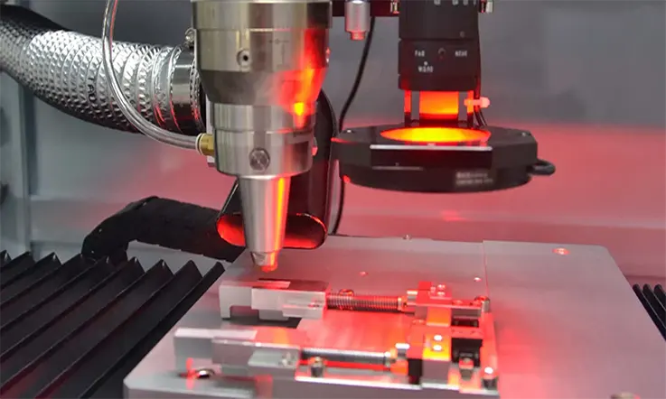
When performing laser drilling, a stationary machine with a high-density laser beam is used to ablate a hole into a printed circuit board (PCB). This technique makes use of the same kinds of materials as traditional mechanical drilling does. The kind of material that needs to be sliced can require one of several distinct varieties of laser.
The laser drilling technique has a number of drawbacks that need to be considered. It may be difficult to achieve accurate depth control if there is not a metal stop layer, and tapering may be the outcome if the ratio of depth to width is particularly high. The fact that it carbonizes the edges that it cuts, which typically results in a black or burnt appearance, is a drawback of the process.
Why Do We Need Laser Drilling in PCB Fabrication?
When designing a PCB with HDI technology, there are typically quite a few microvias included. These microvias, which have the appearance of being blind structures, have a small size and require precision-controlled drilling for their depth. Lasers are the only tool capable of producing results of this level of precision. Why Is It Necessary to Use Laser Drilling in PCB Fabrication not use Mechanical drilling?
Mechanical drilling is not an option for microvias for a number of reasons, including the following:
● It is accompanied by drill vibration.
● It is not able to drill holes in large quantities with diameters of less than 0.15 mm (6 mil).
● It is incapable of doing the precision-controlled depth drilling required for microvias.
● The method of mechanical drilling takes a lot of time and is very expensive. This does not bode well in an environment where a rapid time-to-market is a key condition for success.
● Due to the fact that selecting the appropriate instruments for mechanical drilling must be done by hand, the procedure is prone to a large number of errors caused by human intervention. This could result in time-consuming and financially damaging restarts, which would have an effect on the total cost and timeframe of the project.
On a thin, flat piece of FR4, FR5, and PTFE-based rigid material, as well as polyimide-based flexible material, lasers are able to drill vias with a diameter of 2.5 to 3 mil. It is possible to use lasers to drill 1 mil vias into an unreinforced dielectric, which means there is no fiberglass present in the material. For this reason, laser drilling is the method of choice when it comes to drilling mirovias.
In addition, mechanical drilling and laser drilling each have their own benefits and drawbacks in the process of creating circuit boards. During the engineering review, your PCB provider will determine the procedures that are required to process your order effectively. At the design level, having knowledge of the steps required to construct a printed circuit board (PCB) is useful for making the processing easier.
What Are the Factors To Take Into Account When Laser Drilling PCB?
During the process of laser drilling, there are several characteristics of the circuit board that need be taken into consideration. Two of the most significant ones are discussed in the following.
1.Non-homogeneity of the Stack-up
When working with lasers, the most important thing to keep in mind is the non-homogeneity of the PCB materials that will be employed in the stack-up. There is a wide range of efficiencies among materials in terms of energy absorption. For instance, FR4 resin is capable of absorbing light energy at the same rate as the glass fibers, but it does so without contaminating the hole it creates. Because BT epoxy resin evaporates at a higher rate than glass, it leaves behind fibers of glass in the hole it creates.
When dealing with conditions such as these, it might be challenging to get total accuracy with lasers. As a result, it is strongly suggested that the homogeneity of the multilayer PCB stack-up be maintained to the greatest extent possible. If we utilize materials that have distinct differences in their optical and thermal properties, the manner in which the laser beams react with those materials will likewise be distinct, which will result in inaccurate drilling.
2.The Thickness of Copper
It is recommended that the top copper layer that is going to be pierced have a thickness that is at least twice as thick as the target copper layer.
Lasers are without a doubt the superior option for etching microvias into printed circuit boards (PCBs), despite the fact that there are a few potential obstacles that could develop. In order to meet the ever-increasing need for smaller board sizes and higher wiring densities, laser-drilled microvias are an essential component in the production of printed circuit boards (PCBs). It is a challenging task to produce smaller holes with a high degree of precision without compromising the board’s structural soundness. Laser drilling is the most effective method for the production of such tiny boards.
To Sum Up
Laser drilling is unquestionably the superior method for producing microvias; however, this assertion is contingent on the aforementioned considerations being met first. The utilization of laser-drilled microvias is only expected to rise in the near future due to the ongoing trend toward shrinking, as well as the high density of wire and components.
JarnisTech is one of the most successful printed circuit board (PCB) and printed circuit board assembly (PCBA) manufacturers in China. Because we have used cutting-edge processes and technologies, we are able to offer you the most superior PCB manufacture and Assembly services. We are in full compliance with the RoHS (Restrictions of Hazardous Substance) rules, which call for extremely high quality requirements to be adhered to. In the event that you have any inquiries, please do not hesitate to get in touch with us by sending an email to [email protected] or giving us a call at 0086-755-23034656.