
A microvia is a small hole drilled or etched in a printed circuit board (PCB) that is used to create a connection between layers of the PCB. Microvias are typically less than 0.006 inches (150 microns) in diameter and are used in high-density interconnect (HDI) PCBs to connect the surface-mount components to internal layers of the PCB.
Microvias are different from conventional vias because they have a smaller diameter and can be drilled using a laser or etched using plasma or chemical processes. The smaller size of microvias enables higher routing density, reduced layer count, and better signal integrity in high-speed and high-frequency circuits. Additionally, microvias can be used in blind, buried, or through-hole configurations, allowing for more flexible PCB design.
Microvia technology has revolutionized the electronics industry, enabling the development of smaller, more reliable, and higher-performing electronic products. Today, microvias are widely used in various electronic applications, including mobile devices, medical devices, aerospace, and defense systems, among others, due to their ability to enable high-density interconnections and miniaturization of electronics without sacrificing performance and reliability.
JarnisTech presents expanded capabilities for PCB fabrication, offering laser-drilled microvias for high-tech applications. HDI PCBs are equipped with microvias and stacked microvias to enable more complex interconnections in advanced designs.
What’s A Microvia ?
Microvias, also known as Micro Via, Micro-Via, μVia, Laser Via, or Laser Ablated Via, are holes that have an aspect ratio of 1:1, as per the updated 2013 IPC specifications. In the past, microvias were defined as holes with a diameter equal to or less than 0.15mm (6mil).
The utilization of microvias as the interconnecting mechanisms between layers in High Density Interconnect (HDI) substrates and Printed Circuit Boards (PCBs) have made it possible to meet the high input/output (I/O) density of modern packages. The objective of the electronics industry is to produce cost-effective, lightweight, reliable, portable, and functional products.
At the electronic component level, this results in components with increased I/Os while having a smaller footprint area, such as flip-chip packages, chip-scale packages, and direct chip attachments. At the Printed Circuit Board and package substrate level, this envisages the use of High-Density Interconnects (HDIs) having finer traces and spaces and smaller vias.
There are several fabrication techniques used for microvias in PCB manufacturing. Some common microvia fabrication techniques include:
Microvia Fabrication Techniques
● Mechanical Drilling: This technique uses a small-diameter drill to create the microvia hole, which is then coated with a conductive layer. This technique is cost-effective for simple microvias and is ideal for single-sided and double-sided PCBs.
● Laser Drilling: This technique uses a laser beam to precisely drill microvias with high accuracy, enabling the creation of complex and high-density interconnects. Laser drilling is suitable for high-end PCBs and applications that require fine-pitch microvias.
● Plasma Etching: This technique uses plasma to etch a precise hole in the PCB substrate, which is then filled with a conductive material. Plasma etching is useful when the aspect ratio of the microvia is high, and the diameter is small.
● Photo Imaging: This technique uses photoresist material to create a mask that defines the microvia shape. The substrate is then exposed to light, and the unexposed photoresist is removed, leaving behind the required pattern. The remaining photoresist material is then used to etch the microvia hole.
● Stacked Microvias: This technique uses several layers of small-diameter microvias stacked together to create a larger interconnect. This is a useful technique for high-density interconnects and complex PCB designs.
The appropriate microvia fabrication technique depends on the specific application requirements, such as aspect ratio, size, and layers. The complexity of the PCB layout and the final application of the PCB also play a significant role in selecting the microvia fabrication technique.
Types of Microvias
For PCB manufacturers, there are various options available when it comes to drilling microvias. Each microvia has consistent dimensions, with the primary differentiation being its location.
PCB design engineers can choose from various microvia types, including:
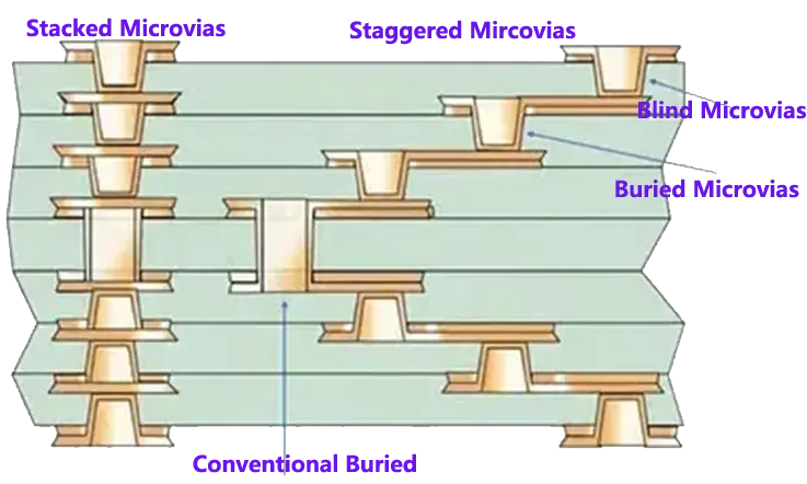
● Via In-Pad Microvias: These microvias are positioned directly onto the copper solder pad, enabling PCBs to be downsized.
● Staggered microvias: Staggered microvias are layers with numerous buried microvias arranged at staggered intervals. These microvias are offset from one another, rather than stacked side by side.
● Stacked microvia: Several blind or buried microvias are stacked on top of one another to connect the inner layers.
● Buried microvias: Microvias are holes buried in the inner layer of the printed circuit board (PCB) that do not reach the surface of the circuit board.
● Blind Microvias: These holes facilitate connections between the surface and an interior layer, but do not extend through the board’s thickness. Unlike through-holes, they only penetrate one side of the board.
Size of Microvia
In PCB design, the stack-up must be established prior to microvia size decisions in terms of both diameter and depth. The designer needs to determine the layer count suitable for accommodating the routing of fine-pitch BGAs and BGA fan-out. After the stack-up is established, the two parameters are the only ones needed to determine a compromise between routability and access to fine-pitch components: the microvia diameter and depth.
The IPC standard can be used to determine the diameter of the pad, which is dependent on the product class. Meanwhile, microvia depth is influenced by the layer stack and the required dielectric thickness for HDI routing.
Determining the number of thin outer dielectrics needed is commonly achieved by analyzing the ballout of the largest BGA component on the circuit board. The number of row and column groups offers an indication of the overall number of HDI layers required. Once the number of layers is found, comparison with a core/dielectric material pair is made to enable HDI routing.
These thinner dielectrics can provide regulated impedance needed to support dense, high-speed digital components.
After the layer thickness is established, it’s necessary to place an upper limit on the microvia aspect ratio for reliability assurance. The pad size should be chosen to form a reliable connection with a BGA component, which can be fitted between or beneath the solder balls of the finest pitch BGA. Selecting these dimensions places some restrictions on the microvia layer increments to maintain a specific aspect ratio. By choosing the smallest BGA pitch size to determine microvia dimensions, the microvia is guaranteed to fit beneath any larger pitched BGAs, and larger pad sizes can also be used for coarser BGAs to ensure reliability.
To ensure a dependable connection to a BGA component, proper pad size and placement are essential. The pad size should permit insertion of the pads between or beneath the solder balls on the board’s finest pitch BGA. This approach may restrict the thickness of the layers utilized for microvias with the finest pitch components to retain a specific aspect ratio. By using the BGA with the smallest pitch as a reference, the microvia size can be selected to fit beneath any BGAs with a larger pitch. In the case of coarser BGAs, employing larger pad sizes may be necessary to ensure reliable connections.
Advantages Of Microvias
● PCB designers may reap several benefits from incorporating microvias into their circuit board designs. The use of microvias enhances the board’s functionality and performance by delivering thermomechanical reliability. The ability to manufacture via-in-pad microvias results in circuit board miniaturization, which is critical for mobile devices. Moreover, microvias save space on the circuit board as they are smaller than conventional vias and plated-through holes. This space conservation enables the board to fit in smaller components.
● Since lasers are employed to drill microvias, PCB designers can minimize the risk of manufacturing issues. Reducing trace lengths decreases fabrication difficulties. Microvias have a significant impact on signal integrity when designing HDI circuit boards. The radiation amount produced by high-speed circuits decreases when smaller vias are implemented. The placement of microvias improves RF capabilities and EMC properties. Compared to other types of vias and through holes, microvias have superior reliability.
Disadvantages Of Microvias
Some possible disadvantages of microvia PCBs are:
● Higher cost: Microvias can be more expensive to manufacture than traditional vias, mainly because they require more advanced manufacturing techniques.
● Limited depth: Microvias are typically shallower than conventional through-holes, which can limit their use in some applications.
● Quality control: The small size of microvias can make it more challenging to ensure consistent quality during manufacturing, which can lead to reliability issues if not properly controlled.
● Plating limitations: The plating of microvias can be more challenging than that of conventional vias due to their smaller size, which can result in poor plating quality and reliability issues.
● Design complexity: The use of microvias can increase the complexity of PCB design, as care must be taken to ensure proper placement, routing, and via density to avoid signal integrity issues and manufacturing defects.
Reliability of Microvia
● The reliability of HDI structures is a primary challenge in achieving their successful integration into the PCB industry. High thermo-mechanical reliability in microvias is required to ensure satisfactory HDI reliability. Multiple researchers and professionals have probed the reliability of microvias in HDI boards by examining microvia geometry parameters, dielectric material properties, and processing parameters.
● Most research on microvia reliability has concentrated on experimental assessments of the dependability of single-level, unfilled microvias, as well as finite element analyses of stress/strain distributions in single-level microvias, which estimate microvia fatigue life. Interfacial separation (the separation between the base of the microvia and the target pad), barrel cracks, corner/knee cracks, and target pad fractures (also known as micro-via pull out) are the most common types of micro-via failures identified.
● Thermomechanical stresses resulting from a mismatch in the direction of the PCB thickness between the metallization in a microvia structure and the surrounding dielectric materials cause these failures. This mismatch is determined in terms of the coefficient of thermal expansion, or CTE.
Capabilities of Microvia in the Printed Circuit Board
Microvias in PCB design serve as a crucial means of establishing links between different board layers. Two common types of microvias are traditional microvias and via-in-pad microvias, which have minor differences.
Via-in-pad microvias are placed directly onto the solder pads, which has a significant impact on circuit board miniaturization. This downsizing is necessary for maintaining the functionality and integrity of the printed circuit board.
Using microvias, engineers and technicians can create circuit boards with smaller Ball Grid Array (BGA) pitches. During PCB component layout design, BGA pitches are a critical consideration. Larger BGA pitches must be accounted for in the layout, which can be challenging when installing larger holes. However, microvias do not require greater BGA pitches on other sides due to their small size.
Microvias enable the creation of high wiring density in PCBs, which is yet another outstanding ability they possess. Using microvias is also a cost-effective approach to boost the wiring density of a PCB. In addition, microvias are believed to be the simplest means of achieving this goal.
When Designing Microvias on Printed Circuit Boards
Drilling microvias is a complex process with various considerations in printed circuit board (PCB) design. While designing a circuit board, it is essential to keep the microvia’s aspect ratio at 1:1 or less if a reliably plated hole is desired. Although drilling microvias with a higher ratio is possible, it can result in plating errors, making it unreliable.
Furthermore, our PCB designers strictly abide by a minimum diameter of 4 mil for microvias. While using a laser drill for copper surface drilling, any copper over half an ounce in weight is unsuitable as thicker copper necessitates more effort from the laser to create and ablate the hole down to the subsequent layer.
Each layer with a microvia must undergo an additional lamination phase if placed in multiple layers. When unneeded holes are present, they can be filled with nonconductive material or plated shut. The small size of microvias may not require filling as they are typically plated with copper. The plating process for copper requires a specific bath and chemistry. Fabricating with this method allows for greater design flexibility.
In cases where a layer is skipped, such as in the case of blind microvias from the first to the third layer, clearances are necessary alongside the second pass-through layer. However, if the second layer needs to be connected to the third layer, stacked or staggered microvias can be applied. Staggered vias are a reliable and simpler option to construct.
Applications of Microvia PCBs
Microvia PCBs are widely used in various electronic applications, including:
● Smartphones and Tablets: These devices require high-density interconnects to accommodate multiple functionalities in a small space, making microvia PCBs an excellent choice.
● Wearable devices: These devices have size limitations and require PCBs with smaller footprints, making microvias an ideal solution.
● Aerospace & Defense: Microvia PCBs are used in advanced radar systems, satellite communications, and other aerospace and defense applications requiring high-frequency high-density interconnects with reduced weight and size.
● Medical devices: Microvia PCBs can be used in medical devices such as pacemakers, medical implants, and sensors that require high-density interconnects and biocompatible materials.
● Automotive: The increasing complexity of modern vehicles requires smaller and lightweight electronic components, which can be achieved using microvia PCBs.
● Industrial Automation: Microvia PCBs find applications in various industrial automation control circuits, such as motor control, sensors, and power management systems.
● Consumer Electronics: Microvia PCBs are used in various consumer electronics including televisions, cameras, MP3 players, and game consoles that require small size and high-density interconnects.
Overall, microvia technology is rapidly evolving and being adopted in various electronics applications, as it enables high-density interconnects and miniaturization of circuitry without compromising on performance and reliability.
Future trends in Microvia Technology
Some possible future trends in microvia technology include:
● Smaller Microvias: The trend towards miniaturization of electronic devices is driving the development of microvias that are smaller in diameter and depth. This may include the use of lasers to create microvias with greater precision and accuracy.
● High-density Interconnects: The use of microvias can enable the creation of complex high-density interconnects (HDI) with reduced layer count, smaller footprints, and improved signal integrity. This can lead to smaller, more reliable, and higher-performing electronic products.
● Embedded Passives: Microvias can also be used to embed passive components (resistors, capacitors, and inductors) directly into the PCB substrate, reducing the overall size and weight of the board while improving signal integrity and reliability.
● 5G and IoT Applications: As the demand for high-speed and high-bandwidth connectivity continues to grow, microvia technology can play a critical role in enabling the development of 5G and IoT devices that require high-frequency circuits and RF shielding.
● Sustainable Manufacturing: With increasing attention being paid to environmental concerns, the use of green and sustainable materials, such as recycled metals and biodegradable substrates, in microvia manufacturing can become more prevalent. This can further reduce the environmental impact of electronics production.
Summary
Microvias have become an increasingly important aspect of modern printed circuit board (PCB) manufacturing. Microvias enable high-density interconnects, reduced layer counts, and improved signal integrity in complex and miniaturized electronic devices. While there are some challenges associated with microvia technology, including higher manufacturing costs and quality control issues, the potential benefits outweigh the drawbacks. As a result, microvia technology is expected to continue to evolve and play an important role in the development of electronic products for a wide range of applications and industries.
In the manufacturing of printed circuit boards (PCBs), microvias offer a great deal of flexibility to PCB designers, providing increased reliability when connecting multiple layers for customers. When selecting materials for PCBs, it is important to consider materials that are suitable for the microvia drilling process.
It is advisable to engage with the PCB fabricator when selecting the material set to better understand the available options. The experts at JarnisTech have extensive industry experience, and they can offer valuable insights to help customers select materials that suit their respective applications while ensuring seamless connectivity for their electrical components.
Utilizing a variety of microvia drilling procedures can help reduce material costs. By incorporating vias, designers can acquire smaller circuit boards that conserve space. This approach can result in considerable cost reductions while also reducing the risk of manufacturing defects and problems.
It is important to avoid selecting a microvia PCB manufacturer solely based on the lowest price offered. Rather, trust experienced manufacturers with sufficient capabilities. With more than 20 years of experience in PCB assembly and manufacturing, JarnisTech may be the preferred PCB manufacturer in China for your needs. Contact us at JarnisTech to find out how we can help you.
Related Posts:
1. What Is PCB Etching and How to Make a perfect PCB Etching?
2. The Best PCB Panelization Guide
3. The Importance of 3D Printed PCBs in Modern Electronics Production
4. Understanding PCB Delamination: A Comprehensive Guide
5. The Best Backplane Printed Circuit Boards Factory
6. An Overview of Through-hole Technology (THT)
7. Detail Talk Surface Mount Technology
8. PCB Clone : Copy Your Printed Circuit Board
9. PCB Drilling: Definition, Technology Types and Process
10. Castellation PCB Fabrication: Castellated Hole (Plated Half Hole) Technologys Why So Important


