
In the future, high density, multiple functions, and mechanization will become the norm for the exponential rise of electronic gadgets. The board components advance in the form of geometric indexes, but the PCB sizes are getting smaller and smaller, so they have to relate to the board that is supporting them. Due to the presence of a plated PCB half hole, the volume of the round hole will be significantly increased when it is filled with soldering flow and poured into the motherboard. This will cause a cold solder to be produced, which will result in a weak electrical connection between the board and the motherboard.
What are Plated Half-Holes (Castellated Holes) ?
Castellated holes, or plated half holes, are formed by drilling through the edge of copper-plated circuit boards. Its primary application is board-on-board connections, when two printed circuit boards of different technologies are joined together. When compared to a similar connection using multi-pin connectors, the overall system is much more compact because to the direct connection of the PCBs. Therefore, the plated edges are excellent for manufacturing small PCB modules.
Plated half holes can be found on both standard and advanced printed circuit boards (PCB). The minimum diameter of castellated holes required for normal PCB servicing is 0.6 millimeters (mm). If you require castellated holes that are smaller, please speak with one of our overseas salesmen. They would be happy to provide you with professional PCB service.
Half-Holes: How to Design ?
The capabilities depicted in the picture below should be used as a guide in producing half-holes PCBs at JarnisTech. Remembering these rules will help you avoid common mistakes while designing your PCB layout.
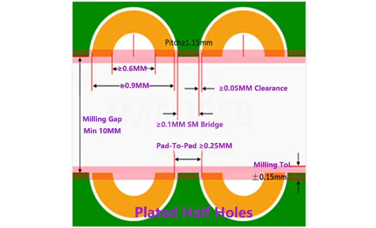
● Min hole pad diameter is 0.9mm.
● Min solder mask bridge is 0.1mm.
● Min Pad-to-Pad distance is 0.25mmm.
● Milling tolerance for holes halving is +/-0.15mm.
● Min drill diameter for forming half-holes is 0.6mm.
● Min solder mask clearance of half-holes is 0.05mm.
● Min feature pitch between two nearby holes is 1.15mm.
● Depending on the intended use of the board, ENIG may be the preferred surface finish.
● There is no limit to the number of half holes, but having a lot of holes makes putting together the PCB easier.
The use of half-holes is possible in both double-sided and multilayer printed circuit boards. If at all possible, you should use holes that are larger than 0.6 millimeters and hole pads that are larger than 0.9 millimeters. When designing plated half-holes on your multilayer PCB, you should try to connect the inner layer pads to the plated holes for halving if at all possible. This will add more stability to the design and will help you avoid burrs.
Castellated Holes: How to Manufacturing ?
After the design of these holes is complete, a one-of-a-kind technique is used to manufacture the product. Prior to the beginning of the manufacturing process, it is imperative that you, as a designer, communicate your requirements to the PCB fabricator. Normal milling tools are not suitable for the purpose of adding these characteristics. Because these half-holes are plated with copper, it is possible for the tools to become damaged while milling. As a result, this calls for millingbits with a higher duty rating. After the milling operation is finished, the holes are deburred, cleaned, and inspected for quality control. Castellated holes make the inspection of connections easier while also facilitating the straightforward installation of modules.
Process:
Drilling- plated through hole (PTH) – panel plating – image transfer – pattern plating – striping – etching – solder mask – surface coating – plated half holes.
When using plated half holes to stack one PCB directly on top of another PCB, there are two requirements that must be met as follows:
● Not only must it have a physical connection, but it also needs to have electrical contacts;
● There is either a gap or no space between the boards.
Plated half holes are an efficient and cost-effective connection technique that can transform a circuit board into a surface-mounted sub-assembly. In most cases, they are utilized in breakout circuits for fine-pitch SMD components or for small radio or RF assemblies. In addition, they are utilized in general. Due to the fact that the boards are concave and coated, they are able to provide a better landing for soldering. These are located on the edges of the PCB supports, which will allow the daughter board or surface mount components to install flush on the surface of the motherboard. If they are properly installed, there will be no room for moisture or dust to accumulate.
The plating half-hole method is not a straightforward drilling procedure; rather, it calls for superior procedures and advanced technological expertise. As a result, additional fees are typically required for plated half-holes. If you are unsure about the details of the plating or the cost of the fabrication, you should get in touch with the manufacturer. In addition, if you have other specifications for the plated half-hole, please get in touch with us through our online service or by sending us an email. You can rely on JarnisTech to supply you with the most effective solutions!
How JarnisTech Helps You Castellate ?
In order to reliably manufacture castellated holes, one must ensure that there is sufficient mechanical strength to prevent delamination and other errors during the manufacturing and assembly processes. We have outlined a set of recommendations regarding how to accomplish that objective in the most effective manner; but, we have left room for some leeway in the event that you, the designer, would choose to implement a different strategy.
● During manufacturing and assembly, we use break-tabs to attach the PCB to a panel. Each tab requires up to 5 mm of edge length, and two are typically placed per edge. As expected, however, the number and placement of tabs depend substantially on the size and shape of the board. If you have castellated holes on two of the four corners of a rectangular board, it is typically not difficult to locate space for these tabs on the other two edges. If these two edges are completely filled with castellated holes and the other edges are also castellated, the best course of action is to contact us for guidance.
● The board’s top and bottom surfaces are required to have a copper annular ring attached to them. The finished hole size + 0.70 millimeters is the minimum pad size that we recommend for use. For instance, if you define the completed hole size as 0.80 mm (our recommended minimum hole size), then the pad size should be a minimum of 1.50 mm. This will result in an annular ring that is 0.30 mm.
● We strongly urge that inner layers likewise keep the same size pad at the annular rings in the surface layers; doing so strengthens the mechanical strength of the castellated hole. This is something that should only be done if it is absolutely impossible to do otherwise. (You should be aware that some EDA tools can ‘optimize’ these away, so you’ll need to find a means to stop that from happening.) Again, get in touch with us if you find that installing inner-layer pads is impossible due to the presence of something that is blocking the way.
● We are capable of manufacturing castellated holes with a finished hole diameter of as little as 0.5 mm, but the diameter of 0.8 mm or bigger is what we propose. Although finished hole sizes more than 1 millimeter can be made with other finishes such as HAL. But, the ENIG surface finish is preferable for castellated holes of any size. In addition, as of the potential for an increase in the number of manufacturing errors, it is our recommendation that the exact half of the hole be left on the PCB. Any other split ratio should be avoided.
To help you digest all that information, we’ve provided a brief synopsis. Make sure there’s place for break tabs; big annular rings on the surface and inner layers strengthen the structure; ENIG surface treatment permits reduction of needed diameters; and it’s ideal to get in touch with us as early as possible to discuss your needs.
Plated Half-holes: Applications and Advantages
Plated half-hole is an economical connection technology that converts the PCB into a surface mount sub-assembly. This technology makes the PCB more reliable. During the process of PCB construction, for instance, a Wi-Fi module or a Bluetooth module might be utilized on its own as a standalone component in order to connect to another board. In most cases, plated half-hole connections are utilized in order to bring together two Boards that make use of distinct technologies. For example, the intricate microcontroller module is joined with a printed circuit board with a universal design. However, we need to be aware that in order for one board to stack on top of another board utilizing plated half-holes, there are two requirements that must be met: first, there must not be any space between the two boards; second, the boards must connect electrically rather than just being physically connected.
Plated half-holes allow for greater design flexibility in PCBs as well as the ability to reduce their size without sacrificing quality. In addition, precisely machined plated half-holes will improve the process dependability of printed circuit boards (PCBs). In addition to this, it can guard the electroplating layer against damage caused by mechanical stress. As a result, printed circuit boards (PCBs) with plated half-holes are utilized in a variety of industries, including high-end consumer electronics, computers, telecommunications, power, automobiles, and industrial controllers, amongst others.
Plated Half-holes: Why do You Require It ?
As stated previously, the major objective is to link the castellated circuit board to various modules. Board-to-board soldering is the technique of soldering a module to another PCB. In board-to-board soldering, castellated holes are required for the following reasons:
● Easy Access and Soldering: Since they are half-holes and are positioned on the side of the module, gaining access to them is relatively simple. Putting SMD pads near the bottom of a module will make it difficult to position components where they need to go. As a result, plated half-holes are included in the design. Because they are located on the edge, the soldering process is simplified.
● Proper Alignment: It is possible for misalignments to occur if the pads are placed underneath a module. However, the likelihood of alignment issues is decreased when the holes are located on the side of the printed circuit board (PCB).
● Easy measurements: It is much simpler to determine the distance between the holes and the solder when plated half-holes are utilized as the measuring tool. Even after the module has been placed, we can use calipers to measure the distance between the two points. If the solder pads are located beneath the module, then this cannot be accomplished.
● Cleaner Board Surfaces: The PCB modules with castellated holes are considered surface-mount sub-assemblies. So, they will fit directly on another circuit board just like an SMD component. Since the connection between the two boards is pretty tight, dust and dirt won’t be able to get in between them.
To Sum Up
At JarnisTech, we are a PCB manufacturing and assembly factory, and we provide from pcb fabricate to components sourcing and PCB assembly one-stop sevice. In the meantime, we have produced a huge number of printed circuit boards with half hole designs for a variety of module products. As a result of our extensive knowledge and ability to maintain excellent quality, the smallest size of half hole that we are able to construct is 0.5 mm. In the event that you require any assistance, please do not hesitate to get in touch with us at [email protected]. We will be more than pleased to assist you.
Related Posts:
1. What Is PCB Etching and How to Make a perfect PCB Etching?
2. The Best PCB Panelization Guide
3. The Importance of 3D Printed PCBs in Modern Electronics Production
4. Understanding PCB Delamination: A Comprehensive Guide
5. The Best Backplane Printed Circuit Boards Factory
6. An Overview of Through-hole Technology (THT)
7. Detail Talk Surface Mount Technology
8. PCB Clone : Copy Your Printed Circuit Board
9. PCB Drilling: Definition, Technology Types and Process
10. Castellation PCB Fabrication: Castellated Hole (Plated Half Hole) Technologys Why So Important


