Castellation PCB technology has become a prevalent assembly technique in the fabrication of PCBs. Its usage is steadily increasing due to the myriad advantages it offers. With the rapid advancement of modern technologies, the demand for Castellation PCB is also on the rise.
JarnisTech, a distinguished PCB manufacturing company, is renowned for its unwavering dedication to delivering products of the highest quality. Our PCBs are trusted and employed across more than 60 countries worldwide. We take pride in leveraging cutting-edge technologies to manufacture PCBs that consistently embody excellence.
Should you seek comprehensive knowledge on Castellation PCB, we invite you to explore our informative FAQ guide. It covers all aspects relevant to castellated PCB, serving as a valuable resource to address your inquiries. We encourage you to peruse its contents and gain a thorough understanding of the benefits and functionality of castellated PCB technology.
What Is A Castellation PCB ?
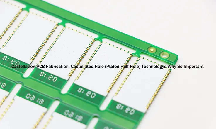
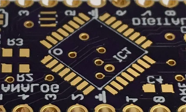
A castellated PCB, also known as a castellated module or castellation board, is a type of printed circuit board (PCB) that features small notches or cuts along the board’s edges, creating a pattern of interlocking teeth. These teeth make it easier to integrate the board with other components or boards, making it a popular choice for electronic devices and modules.
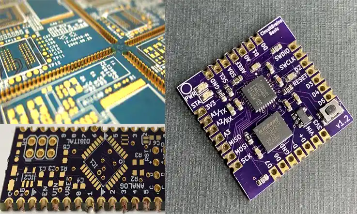
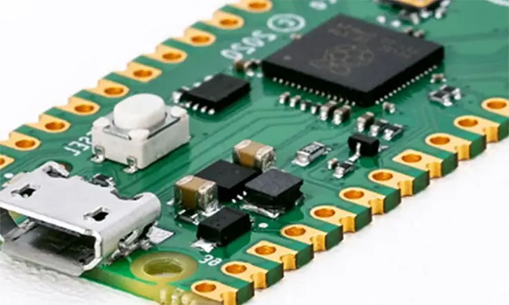
Castellated PCBs are commonly used in applications such as RF modules, Bluetooth modules, and Wi-Fi modules. They can also be used in sensors, cameras, GPS modules, and other electronic devices that require a compact design and easy integration.
Castellated PCBs are typically designed with surface-mount technology (SMT) components, which allow for a smaller footprint and more efficient use of space. They can be manufactured using standard PCB manufacturing techniques, but require additional care during assembly and testing to ensure that the interlocking teeth are properly aligned and secured.
Overall, castellated PCBs offer a versatile and efficient solution for electronic designers who need to integrate multiple components into a small space, while maintaining a secure and reliable connection.
Characteristics Of Castellation PCB
Castellation PCBs have several unique characteristics that make them a popular choice for electronic designers. Here are some of the key characteristics of castellation PCBs:
Interlocking teeth: Castellation PCBs feature small notches or cuts along the board’s edges, creating a pattern of interlocking teeth that allow the board to be easily integrated with other components or boards.
Compact design: Castellation PCBs are designed to be compact, making them ideal for applications where space is limited. They can be used in devices such as sensors, cameras, and GPS modules.
Surface-mount technology (SMT): Castellation PCBs are typically designed with surface-mount technology (SMT) components, which allow for a smaller footprint and more efficient use of space.
Multipurpose: Castellation PCBs can be used in a wide range of applications, including RF modules, Bluetooth modules, Wi-Fi modules, and other electronic devices that require a compact design and easy integration.
Manufacturing: Castellation PCBs can be manufactured using standard PCB manufacturing techniques, but require additional care during assembly and testing to ensure that the interlocking teeth are properly aligned and secured.
Easy integration: The interlocking teeth of castellation PCBs make it easy to integrate the board with other components or boards, reducing the need for additional connectors or cables.
Design Considerations for Castellation PCBs
When undertaking the design of a castellated board, it is imperative to prioritize both high yield and superior quality. The intricate process of designing a castellated circuit necessitates a thorough approach, particularly in relation to designing castellated pads. It is crucial to acknowledge that this process is complex and demands careful attention as even a single costly mistake has the potential to detrimentally impact the overall performance of the circuit board. Consequently, a comprehensive understanding of essential considerations is required for effective castellated pad design.
Half hole PCB
When designing a castellation for a half hole board, PCB designers must be mindful of certain crucial factors. Here are key considerations to bear in mind:
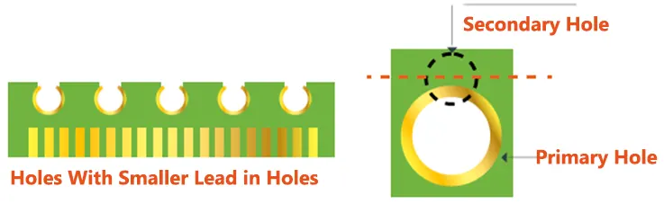
Holes with smaller lead-in holes:
● These holes are highly suitable for connector applications and can be created using a cutting tool. Additionally, they facilitate the creation of smaller castellations as necessary.
Utilize the bottom and top edge for hole placement:
● To ensure the circuit board remains firmly in place, it is recommended to avoid using the vertical edges as locations for the holes. These edges typically serve as bridges, and utilizing them could compromise the stability of the board.
It is important to note that there are various designs available for half holes, which can differ based on the software employed in the design process.
What is Castellated Hole (Plated Half Hole PCB) ?
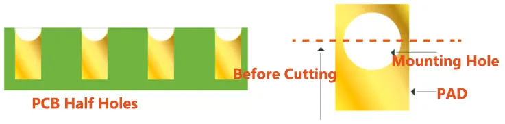
Castellated holes, also known as castellations, are semi-plated indentations located on the edges of a PCB board. They serve the purpose of facilitating the mounting of one PCB board onto another, streamlining the assembly process. Depending on the specific application, these holes may take on the form of partial circles, enabling precise alignment between the two boards.
The presence of castellated holes ensures proper soldering of the boards, particularly in board-to-board soldering processes. These castellations are commonly utilized in various PCB modules, such as Wi-Fi or Bluetooth modules. Despite being separate components, these modules can be mounted together through soldering, facilitated by the castellated holes. This direct connection between two PCBs results in a noticeably slim system, in contrast to bulkier multi-pin connectors.
During PCB assembly processes, Through-Hole Technology and Surface Mount Technology are widely employed. Board-to-board soldering is a common practice when there is a requirement to mount two PCB boards together. Castellated holes play a pivotal role in establishing the connection between the board and the module, bridging the gap between them.
How Many Method to Make Castellated Holes ?
Castellated holes or vias are formed through a standard via process involving the drilling of holes and subsequent copper plating. These holes, shaped like semi-circles, are strategically created on the edges of the PCB by cutting through the board to form partial or half holes. This process allows for openings to be established along the board edges, giving rise to the distinctive appearance of castellated holes. It is worth noting that there exist multiple methods to achieve the creation of castellated holes.
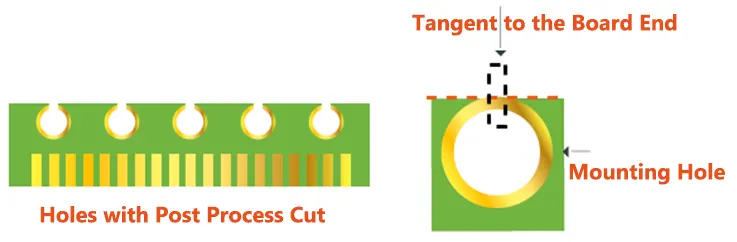
Half Holes
Holes with Smaller cut-in Half Holes
Holes with smaller lead-in holes for post-processing: They are designed for connector applications.
Castellated Holes Manufacturing Techniques – JarnisTech
In the production process of metalized castellated holes, there have been persistent challenges regarding manufacturing defects like copper plating peeling and warping. These defects can lead to unstable solder connections both physically and electrically. In extreme cases, they can also result in short circuits between adjacent pads.
The drilling and plating of castellated holes follow the same procedure as standard plated through holes (PTHs). However, the critical aspect lies in safely removing the opposite half of each hole without damaging the first half or leaving excess copper behind.
JarnisTech, a renowned PCB manufacturer, has developed a detailed process for castellated holes. We ensure that all drill and milling bits approach the board from the correct side while rotating in a clockwise direction. This careful approach guarantees that the copper plating remains pressed against the backing wall during the cutting process. As a result, the unwanted half of the copper ring is cleanly and accurately removed while leaving the other half intact. JarnisTech, the company behind the castellated hole process, has achieved a high level of refinement in our technique.
It is important to note that manufacturing castellated holes is more complex compared to standard PTHs, requiring precision and meticulous handling. Due to the additional drilling process and the often small nature of castellated boards, their production tends to be more expensive.
Stacking Conditions of Castellated Holes
In the realm of PCBs, the term “PCB stack-up” refers to the arrangement of insulating and copper layers that constitute a PCB. The chosen stack-up configuration significantly impacts the performance of the board.
Castellated holes play a crucial role in the process of PCB stack-up. Creating castellated mounting holes is an effective means of manufacturing PCBs intended to be stacked on top of one another. These holes contribute to achieving an excellent printed circuit board stack-up.
It is important to recognize that specific conditions must be met for successful PCB stack-up. Firstly, there should be no gaps or spacing between the two PCBs. The presence of gaps would hinder proper stacking conditions. Secondly, electrical connectivity is essential, going beyond mere physical attachment. Lastly, it is assumed that the size of the upper PCB is approximately one-third that of the bottom PCB.
The aforementioned conditions outline the requirements for castellated-hole-based stacking methods. They provide a foundation for realizing successful PCB stack-up.
Recommended Specifications for Castellated Holes
When incorporating castellated holes in PCB design, it is advisable to adhere to certain recommended specifications:
Size: Utilizing the largest available size for the castellated holes is beneficial as it facilitates proper PCB mounting, ensuring a secure fit.
Pad design: Opting for the largest pad size for each castellation is preferable as it allows for improved compatibility and alignment during assembly.
Distance and diameter: Half holes are suitable for both standard and advanced circuit boards. For standard circuit boards, a minimum hole diameter of 0.6mm is recommended, while for more advanced boards, a smaller diameter can be utilized. Furthermore, it is essential to maintain a minimum distance of 0.55mm between two castellations.
Surface finish: The choice of surface finish plays a significant role in achieving accurate PCB mounting. Electroless Nickel Immersion Gold (ENIG) finish is widely regarded as an excellent option for circuit boards. However, the specific application of the PCB should be considered when determining the most suitable surface finish.
Adhering to these design specifications for castellated holes contributes to the overall effectiveness and functionality of the PCB, ensuring successful mounting and optimal performance.
How to Fabricate a Circuit Board Castellated Pads ?
Here are the steps to fabricate a circuit board with castellated pads:
1. Design the circuit: Design the circuit schematic as per your requirement and choose the appropriate software for PCB design, such as Eagle, Altium, KiCad, or any other of your choice.
2. Define the board outline: Define the board outline with the castellations. This can be done by drawing a line across the board where you want the castellations to be.
3. Add castellations: Once the board outline is defined, add castellations to the board edges by creating small notches or cuts along the edge of the board.
4. Define the copper pour area: Define the copper pour area around the castellations. This will help to create a secure connection between the PCB and other components.
5. Place components: Place the components on the board as per the schematic. Make sure to keep the castellated edge in mind while placing components.
6. Generate Gerber files: Once the design is complete, generate the Gerber files for the PCB manufacturer.
7. PCB manufacturing: The manufacturer will use the Gerber files to manufacture the PCB with castellations.
8. Solder mask: Apply a solder mask over the entire board surface, including the castellations.
9. Copper plating: Apply copper plating on the castellations to make them conductive.
10. Remove the solder mask: Remove the solder mask from the castellations using a laser or chemical etching process.
11. Finish the board: Finish the board by adding components, testing for functionality, and applying a final coat of protective finish.
Overall, fabricating a circuit board with castellated pads requires additional care during the manufacturing process to ensure that the castellations are properly plated and secure. It’s recommended to consult with a manufacturer or expert in PCB design to ensure the board meets your specific requirements and standards.
So Why Castellated Hole (Plated Half Hole) Technology Is Important
Castellated holes on PCBs offer several advantageous features:
Surface mounting: Castellated holes provide a convenient mechanism for surface mounting the PCB onto another PCB or device. The exposed pins can be directly soldered to the required component, eliminating the need for connectors or extra hardware.
Space-saving: The compact and space-saving design of castellated holes is particularly useful in applications where space is limited or when a low-profile connection between PCB boards or components is desired.
Simplified assembly: Castellated holes streamline the assembly process by reducing the requirement for separate connectors or mounting hardware. This simplification can effectively reduce both assembly time and expenses.
Robust mechanical connection: Castellated holes offer a strong and reliable mechanical connection between the PCB and the component. The plated pins provide increased stability and durability compared to other surface-mounting techniques.
Electrical connectivity: The castellated pins establish a dependable electrical connection between the PCB and the components. This direct conductive path ensures proper signal transmission and reduces the risk of signal degradation or interference.
Design flexibility: Castellated holes grant designers greater flexibility, enabling the creation of unique PCB board form factors and supporting innovative product designs. The positioning of the castellated holes at specific locations along the board edge can be tailored to meet specific requirements.
Cost-effective solution: By reducing the need for connectors or additional mounting hardware, castellated holes can contribute to overall cost savings in manufacturing processes. The simplicity of the design and assembly processes can potentially provide a more cost-effective solution.
What Are The Ways To Achieve A Perfect Castellation PCB ?
To ensure optimal mechanical strength in a Castellation PCB, several factors should be carefully considered:
Break tabs: Incorporating break tabs is essential to enhance mechanical stability during the board’s manufacturing and assembly. Break tabs with an edge length of up to 5mm, positioned at two locations per edge, help secure the panel to the PCB. The specific positioning and quantity of break tabs depend on the board’s shape and size.
Copper annular rings: It is advisable to utilize copper annular rings on both the upper and back sides of the Castellation PCB. The minimum pad size should match the finished hole size, ensuring sufficient mechanical stability.
Consistent pad sizes: Maintaining consistent pad sizes on the inner layers and matching sizes in the surface layers at the annular rings is crucial. This uniformity in pad sizes contributes to increased mechanical stability throughout the Castellation PCB.
ENIG surface finish: Selecting Electroless Nickel Immersion Gold (ENIG) as a surface finish improves the functionality of the castellated PCB, regardless of its size. ENIG allows for a reduction in required diameters, optimizing the mechanical performance of the PCB.
Half-hole configuration: Ensuring that half of the hole remains on the castellated PCB is a prudent practice. Deviating from this ratio may increase the potential for manufacturing faults and compromise mechanical stability.
To sum up, allocating space for break tabs, utilizing generous annular rings, opting for ENIG surface finish, and maintaining the half-hole configuration all contribute to achieving superior mechanical stability and reliability in Castellation PCBs.
Conclusion
Having gone through the information presented, you have now gained a clear understanding of the significance of castellated holes in various industries, such as industrial control, automobiles, telecommunications, and computer applications. If you are considering projects involving castellated holes or seeking to leverage castellated hole technology in the production of castellation PCBs, we are here to assist you.
We possess comprehensive knowledge of the manufacturing process and stacking conditions associated with half-hole PCBs. Our expertise will ensure the delivery of high-quality castellated holes that align perfectly with your system requirements.
Furthermore, our products are manufactured to meet rigorous quality standards, including ISO9001, RoHS, and UL. If you are in need of exceptional castellated holes for your designs, we are eager to provide our assistance. Rest assured that we offer nothing short of the best quality castellated holes to enhance your system’s performance.
When the time is convenient for you, please don’t hesitate to reach out to us. We would be delighted to further discuss PCB technology and explore how our services can cater to your specific needs.