
PCB Milling, also known as isolation milling and seclusion milling, is an essential operation that must be carried out in order to guarantee the production of high-quality printed circuit boards (PCBs).
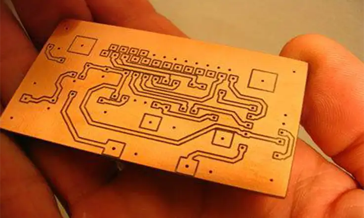
PCB milling is a technique that involves the removal of copper strands from the PCB material. This guarantees that pads are replicated and PCB designs are established. Milling is comparable to etching in that both are techniques that remove material, but unlike etching, milling does not entail the use of any hazardous chemicals. Those lacking a suitable lab setting for etching should consider this option. In addition, etching chemicals are typically caustic and generate toxic fumes when they react with copper traces.
JarnisTech is recognized as one of the most successful printed circuit board (PCB) manufacturers based in China. Because we have implemented cutting-edge processes and technologies, we are able to provide you with the highest quality PCB manufacturing services. We are in full compliance with the RoHS (Restrictions of Hazardous Substance) directives, which require that we adhere to stringent quality requirements.
Send us an email at [email protected] or give us a call at -0086-755-23034656 if you have any questions or concerns regarding the PCB manufacturing services we provide.
PCB Milling: Definition
Printed circuit board milling, also known as isolation milling, is the process of removing areas of copper from a sheet of printed circuit board material. This is done in order to recreate the pads, signal traces, and structures in accordance with the patterns from a digital circuit board plan that is known as a layout file.
PCB milling is a subtractive technique, in the same vein as the more widespread and well-known chemical PCB etching method. This means that material is removed in order to build the necessary electrical isolation and ground planes. PCB milling, on the other hand, is normally a non-chemical operation, and as such it may be carried out in an ordinary office or laboratory setting without the risk of being exposed to potentially harmful chemicals.
When it comes to PCB milling, the quality of a circuit board is primarily determined by the system’s true milling accuracy and control, also known as weighted milling accuracy, as well as the condition (sharpness, temper) of the milling bits and their respective feed/rotational speeds. Other factors that contribute to the quality of a circuit board include the temperature of the milling bits and the feed/rotational speeds. By using the chemical etch technique, on the other hand, the quality of a circuit board is dependent not only on the precision and/or quality of the mask that is used to protect the copper from the chemicals, but also on the state of the etching chemicals themselves.
Therefore, the above manufacturing method can result in the production of circuit boards of a high grade.
In addition, Milling is a type of routing that is performed on the interior of the printed circuit board (PCB), but it is not PCB design. It may be necessary to use mechanical milling in order to carve out the contour of a component, to make place for any mechanical connection, or to construct slots, either NPTH or PTH, in the PCB board. These are all examples of potential uses.
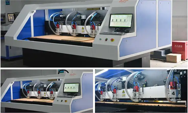
Milling Mechine Tool Types
You will be able to produce GCODE prepared files for the CNC Finder as long as you generate the required Gerber and drill files for your PCB development tools. This will ensure that you are prepared. This step can be easily completed by employing technology developed by a third party that serves a broad purpose and accepts normal Gerber photoplotter data as an interface. As you begin working within this application, you will be given the option to define various surface geometries for milling, cutting, or isolation milling. These operations can be performed simultaneously. Moreover, parameters are provided, which when used to calculate cutting heights and drill diameters, ultimately result in the generation of GCODE for the CNC machine.
As a PCB developer, one of your primary goals should be to ensure that the optimal PCB system design can be accessed in order to give CNC prototype management information for all conceivable established standards and configuration options. Allegro PCB Maker is a CAD solution that comes equipped with tools that flawlessly fulfill this requirement. You are able to fully handle all of the spacing criteria for your subsequent prototype board thanks to the comprehensive and large number of design rules and constraints that are provided by Allegro.
Milling Mechanical Layer in Gerber Files
Just the mechanical information for all layers that are required for the fabrication of your PCB board should be included in the mechanical layer date file. As a bare minimum, it needs to have the following information:
● The precise contours of the PCB board, preferably with dimensions included.
● Details on the precise locations and sizes of any internal machining, slots, or cuts, ideally with dimensions included.
It is best practice to design the outlines using a thin line, for example 0.5mm wide, where the center of the line indicates the exact contour of the PCB board, cut-out or slot, etc.
Notices:
● In the absence of any dimensions being provided, we will always consider the center of the contour lines to be the precise outline of the board.
● It is important to remember not to scale your mechanical layer; instead, it should be 1:1 and match the precise measurements of the PCB.
● In the event that your PCB contains cutouts or slots, it is necessary to include this layer in the fabrication process.
● Like with the other layers, the mechanical layer is viewed from the top to the bottom of the PCB.
● Do not mirror or rotate the mechanical layer.
● Provide only the necessary information in the mechanical layer.
Milling VS Etching
● The use of film or direct laser imaging is typically necessary for chemical grafting, despite the fact that the grafting process itself is quite inexpensive and common in the production of printed circuit board systems all over the world.
● Isolation milling is a process that does not require film art, but it does result in high tooling costs and problems with the application. Isolation milling is so much more crucial for prototypes in the beginning and on an individual basis because of this reason.
● Because the FR4 carrier is not etched, there are no complications associated with the etching process.
● When two systems of isolation are superimposed atop one another, a V-score is generated.
PCB Milling: Adavantages
It goes without saying that PCB milling offers benefits for both the prototyping of printed circuit boards (PCB) and certain specialized PCB designs. The fact that the circuit board does not need to be fabricated using chemicals is possibly the most significant advantage.
On one side, it requires to take time to outsource as constructing a prototype. The second option is to produce a circuit board within the company itself. Using the wet process for in-house production would, however, provide certain challenges with regard to the chemicals and the disposal of those chemicals. Even though it is challenging to manufacture high-resolution circuit boards using the wet method, the base material must first be drilled, and then the circuit board itself must be cut out from the base material.
On the other hand, CNC machine prototype may deliver a quick turn PCB fabrication together with a fast lead time without the requirement of any wet processing. If a CNC machine is already being used for drilling, then this same machine may also carry out the milling and cutting steps of the operation, completing the entire procedure with just one machine. In addition, a CNC machine can be used to do operations such as milling, drilling, and cutting.
Many circuit boards that are simple for milling will be difficult to complete by wet etching and manual drilling in a laboratory setting if you do not employ top-of-the-line technologies that typically cost multiple times as much as CNC milling machines.
However, since the use of CNC is already commonplace for drilling the circuit boards, milling is likely to displace etching in PCB mass production.
PCB Milling: Design Parameters
For PCB board contour or internal cutouts, do not supply actual routing or milling layers. Routing and milling information is product-specific and dependent on the route tools, tool compensations, routing sequence, and routing direction utilized by the PCB fabricator. This means that we cannot utilize routing or milling data supplied by the customer. We must recreate them from scratch, which might lead to confusion or misinterpretations that result in improperly routed PCBs. As PCB manufacturer, it is our responsibility to prepare the correct production routing and milling layers depending on the information in your mechanical layer.
A comprehensive guide to the design parameters that are involved in PCB Milling is provided below:
● The PCB milling equipment has a standard diameter of 2 millimeters, and its smallest diameter measures 0.8 millimeters.
● Milling can be done on either the internal or exterior silhouette of the PCB, according on the requirements.
● The rectangle must have round boundaries. It is crucial that each intersection in the connected milled area be pierced.
● The PCB’s skeleton and separations are machined because if they weren’t, the PCB board’s strength may suffer. Moreover, the PCB board’s internal and external silhouettes require a layer width of 1 micron.
Additional Milling Information
The following additional information should be included in your mechanical layer data if applicable.
● Drill Position Symbols: utilizing symbols to indicate each drill’s location. For every various drill size, utilize a different symbol from the drill map.
● Reference Hole: The distance between one drill hole in X and Y to the outline of the printed circuit board (PCB). This is of utmost significance in situations in which the only holes available are NTPHs and there are no copper pads.
● PTH/NPTH Indication: Please specify which holes and slots are PTH and which are NPTH in the diagram.
● Customer Panels: In the event that you supply panelized data, ensure that you include the appropriate indications for break routing and/or V scoring.
● Layer Sequence: For every copper, solder mask, and silkscreen layers, a clear layer sequence or buildup drawing. Include add any additional layers, such as carbon or peel-off. Provide the right order, seen from top to bottom, together with the right associated data file names.
PCB Milling Process
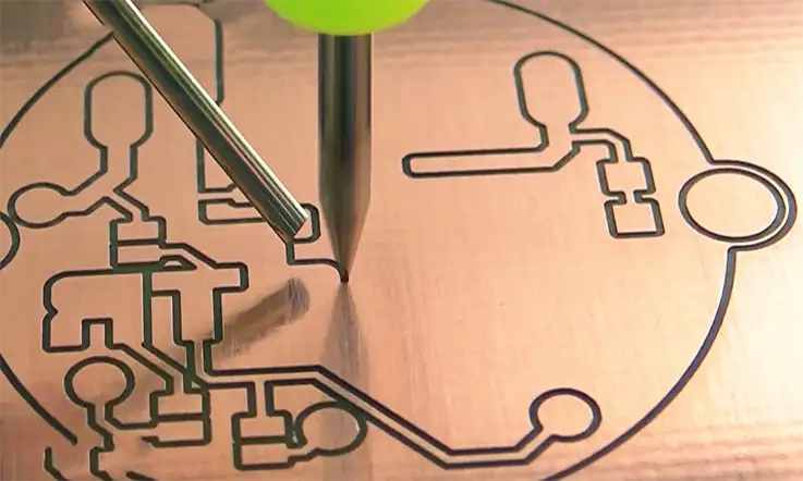
Profiling the printed circuit boards and cutting them off the production panel, either by V-scoring or routing, is the final phase of PCB fabrication. We employ a computer-controlled milling machine or “router” for profiling.
First, the machine begins by milling off any minor slots or internal cutouts. The cutter adheres to the stated routing path in the tool file.
Then, the milling head then automatically selects a 2mm cutter, determines the diameter, and mills around each Board. The brush surrounding the milling head guarantees that the vacuum system collects all of the generated dust. The circuit boards are held in place by tiny material bridges (routing-tab). We will drill through these and then remove each PCB from the production panel individually. Also V-scored is this section.
PCB Milling: Tips for CNC
PCB Milling provides a solution that is both cost-effective and efficient for the production of sturdy boards. Nonetheless, it is essential to adhere to these guidelines in order to guarantee that the method will be successful:
● Leveling: While removing the metal layer from the circuit board, it is vital that a uniform level is obtained. There are two methods for leveling: physical leveling and computer leveling. Physical Leveling is performed using a CNC machine with a floating head. A constant spacing is maintained between the milling tool and the board. Computer Leveling provides an additional method for obtaining a uniformly milled PCB. With this leveling, the distance between the board and the surface is controlled using software.
● Track Clearance: Significant consideration must be given to the track clearance. Normally, a track clearance of 0.5 mm is utilized.
● G-Code Files: It is essential to have a G-code file for each of the operations that can be performed by a machine that is capable of milling, drilling, and cutting.
● Coating: Because the milling process exposes the copper to the possibility of eroding, it is critical to apply a solder mask.
● Safety: When drilling fiberglass, dust will be produced. It is essential that the dust not be inhaled. To accomplish this, a vacuum cleaner should be utilized. You can also avoid this issue by utilizing FR1 and FR2 copper-clad boards that are not dusty.
To Sum Up
JarnisTech is one of the most experienced manufacturers of PCBs and PCB assemblies in China. We has been a market leader for more than 20 years. Not only are we highly specialized in quick-turn PCB prototype fabrication and PCB assembly, but we are also highly specialized in medium and small volume PCB fabrication. We are also committed to adhering to the highest standards in PCB fabrication and assembly, and we employ the most cutting-edge PCB milling equipment available to fabricate your circuit boards. This ensures that the boards will be of the finest quality possible to fulfill your requirements.
In the event that you require any assistance, please do not hesitate to get in touch with us at [email protected]. We will be more than pleased to assist you.
Related Posts:
1. Why Blank Printed Circuit Board Need to Milling?
2. What Is PCB Etching and How to Make a perfect PCB Etching?
3. The Best PCB Panelization Guide
4. The Importance of 3D Printed PCBs in Modern Electronics Production
5. Understanding PCB Delamination: A Comprehensive Guide
6. The Best Backplane Printed Circuit Boards Factory
7. An Overview of Through-hole Technology (THT)
8. Detail Talk Surface Mount Technology
9. PCB Clone : Copy Your Printed Circuit Board
10. PCB Drilling: Definition, Technology Types and Process
11. Castellation PCB Fabrication: Castellated Hole (Plated Half Hole) Technologys Why So Important


