
At various points in one’s life, one could have different opportunities or choices presented to them. This is something that is inherent in human nature. It has repercussions for things like products, designs, and applications, among other things. When conditions like this arise, it is absolutely necessary to conduct research on the various changes in order to satisfy demand.
The electronic and electrical industry is not exempt from the change drive being implemented. The widespread adoption of PCBs makes it unavoidable that the manufacturing process will undergo change. One of the essential needs is that the PCB edge plating be completed. It is a precaution that was taken to ensure the safety of powerful connections made through the PCB. The use of PCB Edge plating helps reduce the likelihood of problems that are difficult to fix.
Edge Plating & Border plating & Castellation & Sideplating
PCB edge plating is a strip of protective metal that is manufactured on the narrow side of the board. It is also known as border plating, side plating, castellation, side metal, and plated contour. Other names for this type of plating are plated contour and plated border. Depending on the requirements of the design, a circuit board may have only one side edge plated or it may have plating all around it. Due to the fact that it safeguards both the electrical performance and the physical integrity of a circuit board, the usage of this additional metal wasn’t quite as common in the past, but in recent years, its application has seen a rise in popularity. Continue reading if you are thinking about using PCB edge plating in your next layout so that you can learn more about what it is, how it is manufactured, and some of the design constraints that you need to be aware of.
How to Definition of Edge Plating for IPC standards ?
According to the rules of the IPC, the term “edge plating” does not have a definition. Notwithstanding this, edge plating is typically understood to refer to copper plating that extends from the top to the bottom surfaces of a PCB board as well as along at least one of the board’s perimeter edges. This definition is usually accepted. Electric conduction is enabled by the copper plating on the edge, and the space between the two boards offers an opening that can be used for mounting multiple boards or embedding edge connectors.
PCB Plated Edges: Design Rule
It is needed that the plating not only engulf the edge of the panel, but that the plating also wrap around to the surface of the panel. In other words, the plating must be wrapped around the panel. Figure 3 illustrates this concept, and the required minimum distance that the plating must wrap around to reach the surface is 0.015 inches. The wrap-around is essential for both the processing done on the inside and the adhesion of the plating to the edge. Furthermore described is the closest that a feature can be placed to the wrap around plating (0.010 inches), as well as the minimum space that must be maintained between adjacent routed features (0.100 inches).
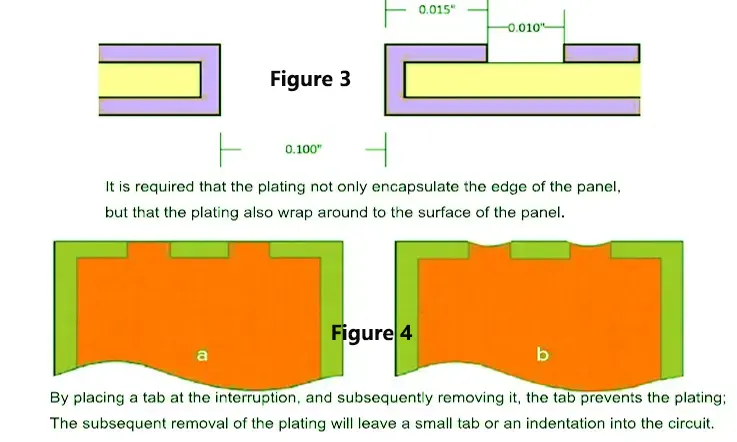
It is customary for the plating to be continuous over the entirety of the edge of the circuit; however, interruptions in the plating can be designed using either of two different approaches. Placing a tab at the interruption and then removing it stops the plating from happening (Figure 4a).
Instead, the plating interruptions can be eliminated at the last phases of the routing process. After the plating is removed, the circuit will have a little tab or an indentation in it (Figure 4b).
The indentation is produced when the router bit makes contact with the edge of the circuit where the plating is being removed and then continues forward into the circuit in order to completely remove the coating. When there will be an interruption in the plating process that is at least 0.200 inches long, using a tab to break up the plating process can be done. If it is less than 0.200 inches, the edge will be plated completely across, and then the routing procedure will be used to remove the plating.
In most cases, edge plating requires the joining of one or more of the internal planes that are contained within a board. The plating procedure ensures that these planes are electrically connected to one another and that they reach all the way to the board’s edge. When these layers are routed and removed from a panel, there is a risk of exposed copper, hence they are normally constructed with a polarity border (refer to 0.050″) to prevent this risk.
Figure 4: a) The plating can be prevented by placing a tab at the interruption and then subsequently removing the tab; b) the plating can be removed in a subsequent step, which will leave behind either a small tab or an indentation in the circuit.
It is essential to have a strong understanding of the cost drivers in PCB fabrication as well as early involvement between the designer and the fabricator in order to achieve success in designing a product that is cost-effective. The first step is to ensure that you are following the DFM requirements provided by your fabricator.
Circuit Board Edge Plating: How is Fabricated ?
The plating of the edges of circuit boards is a very routine operation that is typically performed as an extension of the standard plating methods that are utilized in the manufacture of circuit boards. It is necessary to mill the outer edges of the board that are going to be metalized prior to plating the surface and the thru-holes of the board. This will make it possible for the edges to be plated simultaneously.
Unfortunately, getting the metal plating to stick to the board edges might be difficult at times. In order to make certain that the plating procedure is successful and achieves the desired results, the board’s edges will need to be prepped by eliminating any defects and smoothing them out. It is also vital to incorporate a metal strip into the design of the top and bottom layers of the board so that it can function as an anchor for the edge plating to adhere to.
Copper electroplating is an option for the board’s metalized edges; doing so will reduce the overall cost of edge plating because the procedure will already be in use for the other areas of the board. Other fabricators may utilize electroplated nickel and gold, immersion gold or silver, or a combination of the two. Immersion silver or tin, hot air solder leveling (HASL), and electroless-nickel immersion gold are some of the surface finishes that can be applied to the plating after it has been completed. Another option is to use immersion gold (ENIG).
Therefore, Before committing to PCB edge plating, it’s crucial to understand its limits.
Issues That Need To Pay Attention to Edge Plating
● It is possible for the metal edge to peel if the surface of the board’s edges is not appropriately prepared for the plating process. This is because the adhesive strength will not be sufficient.
● It is not possible to remove circuit boards from their manufacturing panels using V-scoring if the boards are going to have edge plating put to them.
● When a manufacturing panel is utilized to process the circuit boards, there will be gaps in the metal plating at the locations where the breakout tabs are employed.
● The area that needs edge plating should be marked clearly in the mechanical layer before fabrication.
● Metallization cannot be performed at the location of the small bridge.
● No internal power planes get to the board edge.
● Ensure enough space on edge for side plating.
● Any burrs that are left over from the milling process can cause the plating procedure to fail, and they need to be thoroughly smoothed away before the metal edge is applied.
JarnisTech has been a market leader for more than 20 years, and as a result, we have a great deal of manufacturing expertise for PCB edge plating. As a result, we are able to control a high quality for edge plating that is free of burrs. We are committed to adhering to the most stringent standards in PCB fabrication and assembly. Our first objective is to ensure that the needs of our clients are met, thus we will do all in our power to ensure that the board we fabricate for you is of the highest possible quality.
Edge Plating PCB: Process
As you are aware, preparing the plated edges and ensuring the long-term adhesion of the plated material are major issues for PCB manufacturers. In addition, edge PCB soldering requires precise handling during PCB assembly. JarnisTech can guarantee that the PCB edge castellation has completely prepared edges surfaces, which then applies the plated copper for rapid adherence and processes the circuit board to make certain of the long-term adhesion between each layer.
During the fabrication of printed circuit boards, it goes without saying that we are able to control the possible danger posed by plated through hole and edge plating by utilizing a regulated procedure for edge soldering. Thus, the generation of burrs is the primary cause for concern. Burrs lead to discontinuities in the plated through hole walls and reduce the edge plating’s ability to adhere for an extended period of time.
PCB Edge Plating: Layout Suggestions
● Although designing a circuit board for edge plating is not difficult, the designer must be aware of a few aspects. First, a metal strip on the surface layers is needed for the plating to connect with. The designer must not only include the metal strips in the layout data but also remove the solder mask in order to expose the metal strips to plating.
● Planning the arrangement of the internal plane layers is another crucial design factor. Although the ground plane is often attached to the edge plating, it is crucial to pull the power plane’s boundary away from the board’s edge. The possibility that the power plane will make contact with the PCB edge plating during manufacturing and result in a direct power to ground short will be eliminated by pulling back the power plane boundaries.
● With the production drawings, PCB designers are required to convey their intentions for the edge plating. In the documentation, you need to define the sides of the board that are going to be plated, the overlap of the edge plating with the metal strips on the surface layers, as well as the type of plating and surface finishes that are needed. You can get assistance with these decisions from a reliable PCB contract manufacturer.
When it comes to resolving these and other layout challenges, the design and manufacturing experts here at JarnisTech frequently collaborate with clients. Therefore, On your upcoming circuit board project, please let us know how we can assist you with PCB edge plating as well as any other design and manufacturing considerations that may arise.
Edge Plating PCB: Application
Edge-plated boards are used in a variety of industries, particularly in applications that require improved support for connections, such as for boards that slide into metal casings. These types of boards are also required for certain circuits. Edge plating serves a number of purposes in addition to enhancing the current-carrying capacity of the circuit board. It also enables edge connection and protection, and it makes edge soldering possible, which helps to enhance manufacturing.
Even though edge plating on printed circuit boards is typically a straightforward addition, fabricators still require specialized equipment and skilled employees in order to carry out the procedure. Fabricators need to check that there is a gap before they begin edge plating, and designers need to make sure that internal power planes do not extend all the way to the edge of the board. Because the plating will link to the copper bands, the designers have a responsibility to ensure that there is a band of copper on both the top and bottom margins of the top and bottom side.
Today edge plating PCB is extensively utilized in a variety of industries, particularly in applications that require better support for connections, such as for circuit boards that slide into metal casings. This is especially true in applications that have been around for a long time. In addition, edge plating offers other benefits, which are as follows:
● Provide edge connection and protection;
● Improve the current-carrying capabilities of PCB circuit boards;
● Provide the possibility of edge soldering to improve fabrication.
PCB Edge Plating: Purpose
Printed circuit boards are susceptible to a variety of risks, some of which can be mitigated by applying PCB edge plating. The following are the four primary areas in which the edge plating can be of assistance:
1. Electromagnetic Compatibility
Electromagnetic interference, often known as EMI, can be caused around the edges of multilayer circuit boards by the current that is carried by the power and ground planes. This interference has the potential to radiate outside of the system, which would cause the circuit board to exceed the EMC criteria it is meant to satisfy. It is possible to stop the EMI from radiating by covering the board’s edges with a barrier made of metal plating.
2. Thermal Dissipation
Printed circuit boards have the potential to produce a significant amount of heat, particularly when signal speeds are increased. Typically, thermal vias are used to transfer this heat into an internal ground plane, where it is then spread uniformly over the board. Because the ground plane is connected to the edge plating, it is much simpler for heat to escape through the board’s metal edge and into the surrounding environment.
3. Structural Integrity
A circuit board can be made stronger and more robust by adding metal to its sides. The boards are less likely to suffer physical damage through their regular use. The PCB’s metal sides also give the board more support as it slides into the metal casings and frames of the intended electronic systems. The Board will be protected by edge plating from unintentional physical damage during handling or use.
4. Signal and Power Integrity
The board’s signal and power integrity will be improved by lowering the EMI. The edge plating’s extended grounding will increase current carrying capacity and give high-speed electronics greater shielding.
Summary
JarnisTech has extensive experience with PCB designs requiring edge plating. For technical information regarding the edge plating procedure and parameters, please contact our sales team and we will be able to assist you as needed.
In addition, we offer services such as PCB Prototype, Batch Manufacturing, the purchasing of components, and PCB Assembly (SMT). When it comes to quality, delivery, cost-effectiveness, and any other demanding requests in electronics, we are dedicated to satisfying the needs of worldwide makers in a variety of industries.
Related Posts:
1. What Is PCB Etching and How to Make a perfect PCB Etching?
2. The Best PCB Panelization Guide
3. The Importance of 3D Printed PCBs in Modern Electronics Production
4. Understanding PCB Delamination: A Comprehensive Guide
5. The Best Backplane Printed Circuit Boards Factory
6. An Overview of Through-hole Technology (THT)
7. Detail Talk Surface Mount Technology
8. PCB Clone : Copy Your Printed Circuit Board
9. PCB Drilling: Definition, Technology Types and Process
10. Castellation PCB Fabrication: Castellated Hole (Plated Half Hole) Technologys Why So Important


