
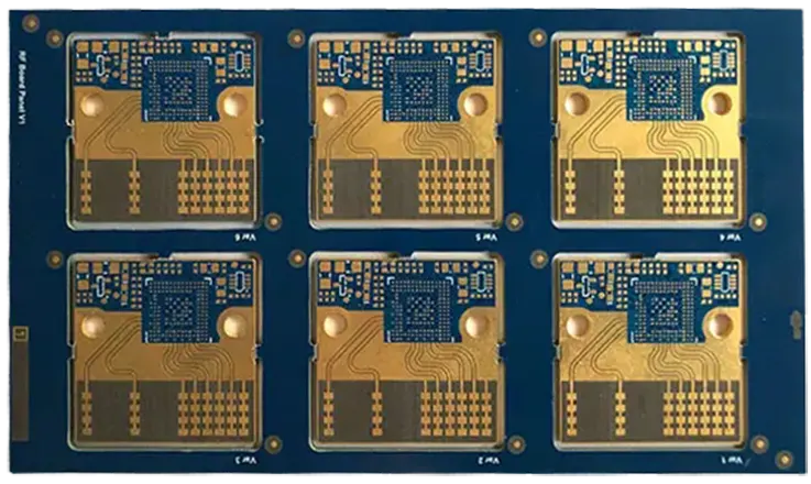
This guide delves deep into all aspects of RF PCB and microwave PCB design, covering everything from design principles and manufacturing techniques to assembly processes and performance optimization. By reading this guide, you’ll learn how to maintain signal integrity in high-frequency applications, optimize production processes to balance cost and delivery timelines, and tackle common design challenges like signal attenuation, reflection, and crosstalk in RF circuits.
Material Selection for RF and Microwave PCBs
The Backbone of High-Performance Designs
When it comes to RF and microwave PCB designs, the choice of material is everything. The materials used in these specialized circuit boards directly influence their performance, from signal speed to thermal management. With high-frequency circuits, the demands on the materials become more complex, and making the right selection becomes key. Let’s dive into the properties and types of materials that make RF and microwave PCBs a success in high-performance applications like 5G communications, military radar systems, and medical diagnostics.
In this section, we’ll dive into the core properties that materials must possess, review the best materials for different applications, and discuss material considerations based on the needs of specific industries.
Core Properties of Materials for RF and Microwave PCBs
Material selection for RF and microwave PCBs isn’t just about durability or cost—it’s about ensuring high-performance. Here’s a deeper look at the essential properties that make a material fit for high-frequency applications.
Dielectric Constant (Dk) and Its Impact on Signal Speed and Frequency Response-
The dielectric constant (Dk) of a material is a key factor when selecting the right substrate for an RF or microwave PCB. Dk influences how fast signals can travel through the material and impacts the frequency response of the circuit. High Dk materials can slow down the signal, making them ideal for specific applications that require low-loss transmission lines and reduced signal degradation. For instance, materials with low Dk values like PTFE (Teflon) are used in high-frequency designs because they help maintain signal integrity over long distances.
A low Dk value ensures that the signal travels at higher speeds and with minimal distortion. If you’re designing a 5G network PCB, you’ll want a material with a consistent and stable Dk across the operating frequency range.
| Material | Dielectric Constant (Dk) | Signal Speed Impact | Best Use Case |
| PTFE (Teflon) | 2.1 – 2.3 | Low Dk, faster signal speed | High-frequency RF, 5G |
| Rogers RO4350B | 3.48 | Moderate Dk, balanced speed | Aerospace, military systems |
| Ceramic-filled | 6.5 – 7.0 | High Dk, slower signal speed | Satellite communication |
Loss Tangent (Df): Minimizing Signal Degradation in High-Frequency Circuits-
Loss tangent (Df) refers to the amount of signal energy lost as it moves through a dielectric material. The higher the Df, the more degradation the signal experiences. This is a big deal when designing microwave PCBs, as keeping signal degradation low is necessary for high-frequency signal transmission. For industries like military and aerospace, where performance and reliability can’t be compromised, materials like ceramic-filled PTFE are often preferred to minimize losses and ensure top performance.
| Material | Loss Tangent (Df) | Signal Degradation | Best Use Case |
| PTFE (Teflon) | 0.002 – 0.003 | Low degradation, ideal for RF | 5G antenna systems |
| Rogers RT5880 | 0.003 – 0.004 | Slight degradation, reliable | Military radar systems |
| Ceramic-Filled | 0.0009 – 0.0015 | Very low degradation | High-frequency medical devices |
For designers, understanding the loss tangent helps in selecting materials that can handle high-frequency applications without reducing signal strength or efficiency. This is a top priority in satellite communications or 5G antenna systems, where precise signal transmission is a must.
Thermal Conductivity: Managing Heat Dissipation in High-Power Applications-
Managing heat is one of the biggest challenges in RF and microwave PCB designs. High-power systems tend to generate heat that can cause components to fail or degrade over time. Therefore, thermal conductivity is an important property of the material used in these designs. Materials with high thermal conductivity, like ceramic-based substrates, efficiently dissipate heat, keeping the system running smoothly and avoiding damage to sensitive components. This is especially true in high-power military systems and medical equipment where overheating can affect performance and lifespan.
| Material | Thermal Conductivity (W/m·K) | Heat Dissipation Efficiency | Best Use Case |
| Polyimide | 0.2 – 0.4 | Moderate heat dissipation | Aerospace, automotive |
| Rogers RT/Duroid | 0.6 – 1.0 | High heat dissipation | Military, satellite systems |
| Ceramic Substrates | 1.5 – 3.0 | Excellent heat dissipation | Medical equipment, high power RF |
Best Materials for RF and Microwave PCB Designs
When it comes to RF and microwave PCB designs, materials aren’t all created the same. To achieve top-notch speed and low loss performance, selecting the right material for your specific needs is the key. Whether you’re working on aerospace, medical, or military projects, the choice of material will have a direct impact on your design’s success. Below are some of the materials commonly used in RF and microwave PCBs to ensure optimal performance.
For high-frequency RF and microwave applications, Rogers laminates stand out as a reliable choice. Options like RO4350B and RT5880 are prized for their steady dielectric properties, low-loss performance, and consistent results in demanding environments. These materials are a natural fit for applications in aerospace, defense, and satellite communication, where every signal needs to stay clean and strong. By reducing signal degradation and ensuring dependable transmission, they help keep even the most challenging systems firing on all cylinders.
| Material | Dielectric Constant (Dk) | Loss Tangent (Df) | Best Use Case |
| Rogers RO4350B | 3.48 | 0.003 | Military radar systems, 5G |
| Rogers RT5880 | 3.66 | 0.003 | Aerospace, high-performance systems |
| Rogers RO3003 | 3.00 | 0.003 | High-speed communication |
For instance, RO4350B is often used in military communication systems where signal integrity and long-range performance are required. Engineers turn to these materials when designing microwave amplifiers, radar systems, or GPS devices.
PTFE (Teflon) and Ceramic-Filled Substrates for Ultra-Low Loss and High-Frequency Stability-
PTFE (Teflon) and ceramic-filled substrates are widely used in high-frequency RF/microwave PCB designs for their low loss and excellent frequency stability. These materials are typically used in applications requiring minimal signal attenuation and high reliability under extreme environmental conditions. For example, Teflon-based PCBs are preferred for 5G antennas because of their low dielectric loss at microwave frequencies.
| Material | Loss Tangent (Df) | Thermal Conductivity (W/m·K) | Best Use Case |
| PTFE | 0.002 – 0.003 | 0.2 | 5G, high-frequency circuits |
| Ceramic-Filled PTFE | 0.0009 – 0.0015 | 1.0 | Satellite communications |
| PTFE-Glass Composite | 0.003 | 0.4 | Medical imaging equipment |
Hybrid Materials: Combining Different Substrates for Enhanced Performance-
Hybrid materials are becoming more popular in RF and microwave PCB design because they combine the strengths of multiple substrates, leading to superior performance. For example, a combination of PTFE with a ceramic filler can provide a PCB that has low signal loss while also maintaining high structural integrity. This hybrid approach is beneficial for high-power, high-frequency systems, especially in telecommunications, aerospace, and automotive radar systems. The combination of materials also allows engineers to fine-tune the thermal conductivity, dielectric properties, and mechanical strength of the PCB.
| Hybrid Material | Advantages | Best Use Case | Performance Benefit |
| PTFE + Ceramic | Low loss, high-frequency stability | Military, aerospace | Improved signal transmission |
| Polyimide + Glass | Flexible, heat resistant | Wearable electronics | Compact, reliable performance |
| PTFE + FR4 | Cost-effective, good insulation | Consumer electronics, 5G | Balance of cost and performance |
Material Considerations for Specific Applications
The material choice often depends on the specific requirements of the application, such as temperature tolerance, mechanical stress, or flexibility. Let’s explore how materials are selected for different RF and microwave PCB applications.
Choosing High-Temperature Laminates for Aerospace and Military Systems-
For systems like aerospace and military radars, the material needs to perform well at high temperatures and in harsh environments. High-temperature laminates such as Polyimide or high-performance PTFE composites can withstand extreme conditions while maintaining the performance of the RF/microwave PCB. These materials are engineered to prevent signal degradation even under high thermal stress, making them ideal for aircraft communication systems and military-grade satellites.
| Material | Max. Operating Temperature | Thermal Stability | Best Use Case |
| Polyimide | 250°C | Excellent | Military systems, aerospace |
| Ceramic-Based | 300°C | Superior | Satellite communications |
| PTFE | 260°C | High stability | Radar and microwave systems |
The Role of Flexible Materials in Compact Designs and Wearable Technologies-
In industries like medical technology and consumer electronics, the trend is shifting toward more compact designs. Flexible PCBs made from polyimide or flexible PTFE offer flexibility without compromising signal integrity. These materials allow for the development of compact, lightweight, and wearable technologies such as wireless heart monitors or smart medical patches that need to be thin and flexible yet still provide reliable high-frequency signal transmission.
Therefore, materials like Kapton and polyimide are widely used due to their flexibility and durability.
| Material | Flexibility Rating | Signal Loss | Best Use Case |
| Polyimide | Very flexible | Low signal loss | Wearable medical devices |
| Kapton | Flexible, highly stretchable | Moderate signal loss | Flexible antennas, sensors |
| PTFE + Flex | Moderate flexibility | Low signal degradation | Compact wireless systems |
Selecting the Right Substrate Thickness and Layer Count Based on Signal Integrity Needs-
Choosing the substrate thickness and layer count for RF and microwave PCBs directly impacts signal integrity. Thicker substrates can reduce signal attenuation, but they also increase material cost and complexity. On the other hand, thinner substrates are often preferred for low-cost applications but require careful impedance control. For high-performance systems, multi-layer designs are used to improve signal isolation and ground plane integrity while keeping the overall size manageable.
| Material | Layer Count | Thickness (mil) | Signal Integrity | Best Use Case |
| Rogers RO4350B | 6-12 layers | 20-80 mil | Excellent | Military, aerospace |
| PTFE | 4-8 layers | 10-60 mil | Very stable | 5G, high-speed comms |
| Ceramic-Filled | 2-6 layers | 50-100 mil | Excellent for high-frequency | Medical and satellite systems |
RF and Microwave PCB Design Guidelines
Designing RF and Microwave PCBs involves much more than simply connecting components. It’s about making sure every line, every material, and every specification aligns perfectly to ensure peak performance, low signal loss, and reliability over time. Let’s dive deeper into the technical aspects of impedance control, thermal management, and design for manufacturability to make sure your PCB is up to snuff.
Impedance Control in RF and Microwave PCB Design
Getting impedance control right in RF and microwave PCBs is the secret sauce for smooth signal flow. If it’s off, you’ll be wrestling with issues like signal reflection and loss that can throw a wrench in the whole system. To keep everything on the straight and narrow, you need a rock-solid approach. Here’s how to fine-tune your design for seamless signal transmission and avoid those pesky disruptions.
Consistent Impedance for Signal Integrity-
In RF PCB design, keeping the impedance steady across the board is like hitting the sweet spot in a high-stakes game. If there’s a mismatch, it’s a one-way ticket to signal reflection and performance hiccups. The aim is to align the characteristic impedance of the trace with the load impedance of the connected components. While 50 ohms is often the gold standard, certain designs might call for tweaks to other values, such as 75 ohms, depending on the specific requirements. Fine-tuning this balance ensures your signals don’t go haywire, keeping everything in sync.
Techniques for Impedance Control-
●Microstrip Line: This is one of the most commonly used transmission line structures. It’s made by routing traces on the surface of the PCB, and the key to controlling impedance here is adjusting the width of the trace and the distance to the ground plane.
●Stripline: This structure provides better isolation for signals as it sandwiches traces between two ground planes. It’s an excellent choice when you need controlled impedance with high reliability and minimal noise.
●Coplanar Waveguide: Similar to microstrip, but with the trace and ground plane placed on the same layer, making it ideal for specific applications requiring tight control over the field distribution.
By carefully choosing between these techniques, you can optimize the impedance for signal integrity and prevent degradation in signal transmission. Here’s a quick comparison in the table below:
| Transmission Line | Impedance Control | Common Use Case |
| Microstrip | Single-sided, simple to manufacture | High-frequency, low loss |
| Stripline | Symmetric, better isolation | High reliability, complex designs |
| Coplanar Waveguide | Compact, high performance | Advanced, tight tolerance applications |
Thermal Management and Signal Integrity
The temperature of your RF PCB can be a deal-breaker for performance. As your circuit heats up, signal integrity starts to suffer, especially in high-power and high-frequency designs. Thermal management is all about keeping the system cool, which not only prevents component failure but also ensures signal stability.
Heat Dissipation Strategies-
Managing heat effectively can make all the difference. Here are some strategies for reducing heat buildup and maintaining performance:
●Thermal Vias: Small vias that connect hot areas of the PCB to other layers with copper pours help dissipate heat efficiently.
●Heat Sinks: Adding heat sinks to high-power components is one of the easiest and most effective ways to manage thermal challenges.
●Substrate Materials: Some materials, like ceramic-filled laminates, have superior thermal conductivity and help in quicker heat dissipation.
EMI Shielding-
Electromagnetic Interference (EMI) can wreak havoc on signal quality in high-frequency designs. This is where shielding comes in:
●Ground Planes: Proper grounding reduces noise and minimizes EMI by providing a return path for signals.
●Shielding Boxes: For ultra-sensitive applications, you might need to encase parts of the PCB in metal shielding boxes.
●PCB Layout Techniques: Avoid running sensitive traces next to high-power traces to minimize crosstalk and signal degradation.
Here’s a quick glance at how different methods can help manage thermal and EMI issues:
| Technique | Purpose | Best Used For |
| Thermal Vias | Heat dissipation | High-power components |
| Heat Sinks | Passive cooling | Power-hungry devices |
| Shielding | Minimize EMI interference | Sensitive RF and microwave systems |
| PCB Ground Planes | Prevent signal interference | High-frequency, noise-sensitive designs |
Design for Manufacturability
When designing RF and Microwave PCBs, you have to consider more than just functionality; the design needs to be manufacturable. Mass production is often the final step, so design for manufacturability (DFM) helps prevent bottlenecks, costly reworks, or even failure to produce your PCB correctly.
Simplifying Complex Designs-
Complex designs can be difficult to manufacture, especially when tight tolerances and controlled impedance are involved. Here are some ways to ensure that your design stays within manufacturable limits:
●Layer Counts: Keep the number of layers manageable. While multi-layer designs are necessary for certain high-density applications, too many layers can complicate manufacturing.
●Trace Widths: Narrow traces can be difficult to fabricate. Ensure your trace width is large enough to be processed by standard manufacturing equipment.
●Via Sizes: Small via holes are challenging and expensive to produce. Using larger vias can simplify the process without compromising performance.
Design Rules for High-Quality Results-
Following design rules ensures the end product meets your expectations:
●Controlled Impedance: Design traces that maintain a consistent impedance across all layers.
●Tolerance Limits: Work with manufacturers to define the tolerance limits for trace width and spacing.
●Test Pads: Include test pads on the PCB to check performance during the manufacturing process, ensuring the signal integrity is maintained.
Here’s a quick checklist for manufacturability:
| Design Element | Considerations | Best Practice |
| Layer Count | Limit to necessary layers | Reduce layers for simplicity |
| Trace Widths | Must align with manufacturing equipment | Use industry-standard width |
| Via Sizes | Smaller vias can increase cost and complexity | Use standard via sizes when possible |
| Controlled Impedance | Ensure consistency for signal integrity | Work closely with manufacturers to define impedance tolerances |
Advanced Manufacturing Techniques for RF and Microwave PCBs
In the world of RF and Microwave PCBs, manufacturing involves precise techniques that require a high level of expertise. These advanced techniques are designed to ensure that every aspect of the PCB, from material choice to testing, meets the stringent demands of high-frequency applications. Below, we’ll cover high-precision fabrication methods, quality assurance, and key considerations that must be taken into account to achieve the best possible outcome in your designs.
High-Precision Fabrication Methods
When it comes to RF and Microwave PCB manufacturing, high-precision fabrication methods are non-negotiable. The complexity of high-frequency signals demands that every trace, via, and layer is crafted to exact specifications. Let’s take a closer look at some of these cutting-edge techniques.
Laser Drilling for Microvias and Fine Traces-
Laser drilling is one of the leading methods for creating microvias—tiny holes used for signal routing on high-density PCBs. For RF designs, microvias allow for better signal integrity by reducing signal loss caused by the longer trace lengths. Laser drilling delivers high precision and can achieve drill hole sizes that are often smaller than 50 microns, making it ideal for compact designs requiring high-density interconnects (HDI).
Automated Optical Inspection (AOI) and X-Ray Inspection-
Ensuring top-notch quality throughout the production process is non-negotiable, particularly in RF PCB manufacturing, where even the tiniest hiccup can throw performance out of whack. Automated Optical Inspection (AOI) leverages cameras and light to comb through PCBs, spotting defects and confirming that every component is sitting pretty where it belongs. Taking it up a notch, X-ray inspection dives beneath the surface to reveal hidden issues—voids, solder joint irregularities, and bonding flaws in internal layers. These checks act like a double layer of insurance, catching potential headaches before they snowball into costly problems.
Here’s a quick look at these methods:
| Fabrication Method | Purpose | Advantages |
| Laser Drilling | Creates microvias and fine traces | High precision, ideal for small, high-density designs |
| Automated Optical Inspection | Scans PCB for defects | Fast, reliable, ensures high-quality production |
| X-Ray Inspection | Examines internal layers and solder joints | Detects internal faults and ensures layer integrity |
Quality Assurance and Testing in RF PCB Manufacturing
To achieve reliable RF and Microwave PCBs, PCB manufacturers rely on advanced testing methodologies. Testing is performed to verify that the board will function as expected under high-frequency conditions and adhere to specifications. The two main testing techniques used are Vector Network Analyzers (VNA) and Time-Domain Reflectometry (TDR).
Use of Vector Network Analyzers (VNA)-
In RF PCB manufacturing, the Vector Network Analyzer (VNA) serves as a go-to instrument for fine-tuning performance. By measuring S-parameters (scattering parameters), it provides a detailed view of how signals behave as they travel through the board—highlighting reflection, transmission, and potential hiccups along the way. This level of analysis ensures that the PCB can keep up with high-frequency demands without breaking a sweat. Whether it’s for 5G networks, military communication systems, or precision-driven medical devices, the VNA helps confirm that the board delivers top-notch performance without unwanted signal loss or distortion.
Time-Domain Reflectometry (TDR)-
TDR is used to measure and verify impedance matching across the PCB. By sending a signal down the transmission line and observing the reflected signal, engineers can determine whether there are any impedance mismatches that could cause signal degradation. Impedance control is especially crucial in RF PCB design, as even slight variations can lead to issues like signal reflection, loss, or distortion.
Here’s how these testing methods stack up:
| Testing Method | Purpose | Best Application |
| Vector Network Analyzers (VNA) | Measures S-parameters to analyze signal integrity | High-frequency testing in communications, aerospace |
| Time-Domain Reflectometry (TDR) | Measures impedance matching and reflections | Ensures signal quality in RF PCB designs |
Key Considerations for RF PCB Manufacturing
Manufacturing RF and Microwave PCBs requires attention to detail and a thorough understanding of the design’s material and structural integrity. There are several considerations that need to be accounted for to ensure a reliable, high-performance end product.
Precision Tolerances for Line Width and Spacing-
In high-frequency circuits, tolerance management becomes a challenge. Narrow line widths and tight spacing between traces are necessary to maintain signal integrity and reduce parasitic effects. Even the slightest misalignment in trace width or spacing can cause signal loss or affect the overall impedance of the circuit, leading to poor performance. Ensuring tight tolerances during manufacturing is essential to keep everything within specification.
Material Uniformity and Layer Bonding-
Material consistency plays a major role in achieving reliable signal integrity. Variations in dielectric materials or substrate thickness can cause significant shifts in impedance or signal propagation speed. Likewise, layer bonding is a key consideration—if layers are not properly bonded, it can lead to delamination or other structural failures, compromising the board’s reliability and performance.
Managing these factors is necessary to create a reliable RF PCB that performs well over time. Below is a breakdown of these considerations:
| Consideration | What to Focus On | Impact on PCB Performance |
| Precision Tolerances | Trace width, spacing, layer alignment | Affects impedance control, signal reflection |
| Material Uniformity | Consistency in dielectric materials and thickness | Ensures consistent signal propagation, reduces noise |
| Layer Bonding | Proper bonding of PCB layers | Prevents structural issues, ensures long-term performance |
How Optimizing Performance for RF and Microwave PCBs: Design to Manufacturing?
Optimizing the performance of RF and Microwave PCBs is no small feat. Achieving top-notch performance involves a detailed process of design refinement and manufacturing precision. Signal loss, reliability, and signal integrity need to be carefully managed at every stage—from design to production. In this section, we will cover strategies to reduce signal loss, enhance durability, and minimize signal interference to ensure your PCB performs like a charm in high-frequency applications.
Signal Loss Reduction Strategies
Signal loss is one of the top concerns when designing RF and Microwave PCBs. As signals travel through traces, they lose strength due to various factors, including material properties, trace geometry, and the frequency of operation. However, by using low-loss materials and optimizing trace routing, signal degradation can be minimized, ensuring higher performance at the desired frequency.
Minimizing Signal Degradation with Low-Loss Materials-
The choice of material is a major factor in controlling signal loss. For example, using materials like Rogers 4350B or RT5880 offers low-loss tangent (Df), which helps in reducing signal attenuation. High-frequency laminates like PTFE (Teflon) also offer low dielectric loss, ensuring that high-speed signals pass through the PCB with minimal degradation.
Optimized Trace Routing for Signal Integrity-
Trace width and spacing are directly related to the signal attenuation. Narrow traces can introduce greater resistance, leading to signal loss. On the other hand, excessively wide traces might result in higher capacitance, affecting signal transmission. By maintaining optimal trace width and spacing, signal attenuation can be minimized. This is especially important for microwave frequencies, where every bit of loss can impact overall system performance.
| Factor | Impact on Signal Loss | Optimized Strategies |
| Material Selection | Low-loss materials minimize degradation | Use Rogers laminates, PTFE, or ceramic-filled PTFE |
| Trace Width and Spacing | Incorrect sizing increases resistance | Follow IPC-2221 standards for optimal trace width and spacing |
| Layer Count and Complexity | More layers can increase signal degradation | Simplify layout and use appropriate signal routing strategiesc |
By choosing the right material and maintaining proper trace design, you can significantly reduce signal loss and ensure your RF PCB delivers exceptional performance at high frequencies.
Enhancing Durability and Reliability
RF and Microwave PCBs face demanding conditions, especially in military, aerospace, and communications systems, where they need to perform reliably in harsh environments. Vibration, thermal cycling, and humidity can compromise their durability and reliability over time.
Using High-Performance Materials for Environmental Stress Resistance-
Selecting high-performance materials is key to ensuring that your RF PCB can withstand environmental stressors. Ceramic-filled PTFE and Rogers laminates not only offer excellent electrical properties but are also resistant to high temperatures and humidity. These materials provide the necessary thermal stability to avoid deformation or failure during thermal cycling and vibration.
Reliability Testing for Long-Term Performance-
Testing thermal stress, humidity, and vibration is crucial to verify the PCB’s reliability over time. Thermal cycling tests simulate extreme temperature fluctuations, which can lead to delamination or component fatigue. Humidity testing ensures that the PCB does not degrade due to moisture exposure, and vibration testing checks the stability of the assembly under physical movement or shock.
| Factor | Impact on Durability | Testing Methods |
| Material Performance | High-temperature and humidity resistance | Use ceramic-filled PTFE or Rogers laminates |
| Thermal Cycling | Repeated heating and cooling cycles cause damage | Conduct thermal cycling tests to simulate real-world conditions |
| Vibration Resistance | Mechanical stress leads to failure | Test for vibration resistance under simulated operational conditions |
These reliability testing methods ensure that RF and Microwave PCBs will continue to function effectively in the long term, even under demanding conditions.
Minimizing Signal Reflection and Crosstalk
Signal reflection and crosstalk are two common issues in high-frequency PCB designs. Reflection occurs when the signal encounters an impedance mismatch, causing part of the signal to bounce back, reducing overall efficiency. Crosstalk, on the other hand, happens when signals from adjacent traces interfere with one another, leading to noise and performance degradation. Let’s explore some ways to minimize these issues.
Proper Impedance Matching to Prevent Signal Reflection-
To prevent signal reflection, it’s crucial to maintain proper impedance matching between the signal trace and the transmission line. The characteristic impedance of the PCB must match that of the connected components, such as microstrip lines or coaxial cables. Controlled impedance design ensures the signal flows efficiently, reducing reflection and signal degradation.
Ground Planes and Shielding Techniques to Reduce Crosstalk and EMI-
To minimize crosstalk and electromagnetic interference (EMI), ground planes should be used to isolate signal traces and provide a path for return currents. Shielding techniques, such as adding a shielding layer or using via fences, can also reduce the effects of EMI and crosstalk, especially in densely packed designs.
| Factor | Impact on Signal Reflection/Crosstalk | Design Strategies |
| Impedance Matching | Mismatch causes signal reflection | Use controlled impedance techniques for consistency |
| Ground Planes | Insufficient grounding leads to noise | Use continuous ground planes to reduce noise |
| Shielding | EMI and crosstalk degrade signal quality | Implement shielding or via fences for isolation |
By implementing impedance matching, using ground planes, and applying shielding techniques, signal reflection and crosstalk can be significantly reduced, ensuring a cleaner, more reliable signal.
Assembly and Integration of RF and Microwave PCBs
The assembly and integration of RF and microwave PCBs is a meticulous process that requires a high level of precision. This phase involves ensuring that all components, from soldering to testing, meet the necessary performance standards for high-frequency applications. In this section, we’ll delve into the process, covering PCB assembly, integration with other components, and the rigorous quality control required to maintain signal integrity.
PCB Assembly for High-Frequency Applications
When assembling RF and Microwave PCBs, there are several considerations that go beyond standard PCB assembly. Surface-Mount Technology (SMT) and through-hole mounting are two primary methods used in these applications. Each has its advantages and is selected based on the specific requirements of the design.
Surface-Mount Technology (SMT) vs Through-Hole Mounting-
SMT is commonly used for high-frequency applications due to its ability to handle fine-pitch components and its compact nature, which is necessary for minimizing signal path length and maintaining signal integrity. It also allows for automated assembly, making it more efficient for mass production.
Through-hole mounting is still used in some cases, especially when the component requires higher mechanical strength, but it is less ideal for RF designs as it introduces additional inductance and can create longer signal paths, increasing the chance of signal degradation.
High-Precision Soldering and Signal Path Integrity-
For RF PCB assembly, the soldering process must be precise. The most common soldering techniques include wave soldering and reflow soldering. In high-frequency applications, any irregularities in the solder joints can cause signal loss and interference, resulting in poor performance. Ensuring proper solder joint formation and avoiding the introduction of parasitic elements such as inductance and capacitance is key. This requires precise control of the soldering process and the use of high-quality materials.
Below is a comparison of SMT and through-hole mounting:
| Method | Advantages | Disadvantages |
| Surface-Mount Technology (SMT) | Smaller footprint, faster, precise, automated | Can be challenging for high-power components |
| Through-Hole Mounting | Stronger mechanical connections, better for large components | Larger footprint, less suitable for high-frequency designs |
Integration with Other Components
The integration of RF and Microwave PCBs with other components such as amplifiers, filters, and oscillators requires precise coordination to ensure that the final product functions as a cohesive system. The goal is to create an RF system that delivers optimal performance while minimizing noise and interference.
Combining RF PCBs with Amplifiers, Filters, and Oscillators-
For an RF system to perform efficiently, each component must be carefully selected and integrated. Amplifiers are used to boost weak signals, filters ensure that only the desired frequencies pass through, and oscillators generate the required signal frequencies. The integration of these components onto a single PCB needs to be done in a way that avoids signal loss and minimizes electromagnetic interference (EMI).
Packaging Considerations-
Proper packaging is a cornerstone of successful RF system integration. It ensures the system remains compact, handles thermal challenges effectively, and stays shielded from unwanted electromagnetic interference (EMI). For high-frequency designs, using thermally conductive materials and those that excel at blocking EMI is a smart move to keep things running like clockwork. Additionally, focusing on efficient heat management across the assembly prevents hiccups in performance caused by excessive heat. A well-thought-out packaging solution ties it all together, helping the system maintain its edge even under demanding conditions.
Here’s how these components come together:
| Component | Purpose | Integration Challenge |
| Amplifiers | Boost weak signals | Must be placed carefully to avoid interference |
| Filters | Remove unwanted frequencies | Must be tuned to avoid signal distortion |
| Oscillators | Generate required signal frequencies | Placement and shielding are critical |
Quality Control and Testing in PCB Assembly
Quality control (QC) is a fundamental aspect of RF and Microwave PCB assembly, as even the smallest defect can affect performance. Various techniques are employed to ensure the assembly meets the required standards.
Visual Inspection for Soldering Defects and Functional Testing-
Visual inspection is the first line of defense against defects in the PCB assembly. Using magnification tools, technicians check for improper solder joints, misplaced components, or any signs of damage. Beyond visual inspection, functional testing is performed to verify that the RF PCB is performing according to specifications. This typically involves testing the signal paths, ensuring that there are no interruptions or distortions.
X-ray Inspection to Detect Internal Layer Faults-
X-ray inspection is an advanced method used to check for faults in the internal layers of RF PCBs, such as soldering voids or delamination. This is particularly important for high-frequency applications where even the smallest imperfection can result in signal degradation. X-ray inspection allows for a thorough examination without damaging the PCB, ensuring that any internal issues are identified and corrected.
Long-Term Reliability Testing-
Once the PCB assembly is complete, it undergoes several stress tests to ensure long-term reliability. These tests typically include thermal cycling and vibration testing. Thermal cycling exposes the PCB to extreme temperature variations to simulate real-world conditions, while vibration testing ensures that the PCB can withstand mechanical stress without performance degradation.
Here’s a summary of these testing methods:
| Testing Method | Purpose | Best Application |
| Visual Inspection | Identifies soldering defects and component misplacement | Ensures assembly integrity at the component level |
| X-ray Inspection | Detects internal faults, like voids or delamination | Critical for high-frequency PCB applications |
| Thermal Cycling & Vibration Testing | Simulates real-world environmental stress on the PCB | Ensures long-term reliability in demanding environments |
Comparing RF and Microwave PCBs with Conventional PCBs
RF and Microwave PCBs and conventional PCBs may appear similar at first glance, but there are substantial differences when it comes to performance, design complexity, and manufacturing challenges. In this section, we’ll dive into how these two types of PCBs differ in key areas, exploring specific use cases, and addressing design and manufacturing hurdles that engineers must navigate.
Performance Differences
RF and Microwave PCBs operate in a very different environment compared to conventional PCBs. While conventional PCBs are designed for a broad range of applications, RF and Microwave PCBs require specialized signal integrity, impedance control, and material properties to perform effectively at high frequencies.
Signal Integrity and Impedance Control-
When working with high frequencies in RF and microwave PCBs, maintaining signal integrity is everything. A small amount of signal loss can quickly lead to issues like reflections or total signal failure. Impedance control helps to keep things on track, ensuring that the signals flow correctly without interference. Unlike regular PCBs, where impedance mismatches might be overlooked, RF PCBs require precise alignment. Microstrip, stripline, and coaxial structures are commonly used to keep impedance consistent throughout the signal path, making sure the data stays accurate from start to finish.
Material Properties-
Materials used in RF and Microwave PCBs differ significantly from conventional PCB materials. For example, FR4, which is widely used in conventional PCBs, is not suitable for high-frequency applications. Instead, high-frequency laminates like Rogers, PTFE, and ceramic-filled PTFE are used for RF and microwave PCBs to minimize signal loss and maintain consistent dielectric properties at high frequencies.
| Factor | RF/Microwave PCBs | Conventional PCBs |
| Signal Integrity | Strict impedance control is a must. Signal loss and reflections need to be minimized. | Less critical. Lower frequencies have more tolerance. |
| Materials | Use of high-frequency laminates (e.g., PTFE, ceramic-filled). | Typically FR4 or other standard materials. |
| Frequency Range | Designed for GHz frequencies and beyond. | Typically designed for MHz ranges. |
Case Study: RF PCB vs. Conventional PCB in Telecom and Medical Applications
Consider the telecommunications industry, where RF PCBs are responsible for handling high-frequency signals in equipment like antennas, base stations, and mobile devices. In these systems, even the slightest impedance mismatch or signal degradation can cause dropped calls, data transmission errors, or range issues. Conversely, conventional PCBs are used in digital signal processing or power supply boards, where high-frequency integrity isn’t as critical.
In devices like MRI machines, RF PCBs are the real heavy-hitters, transmitting those high-frequency signals without breaking a sweat. Regular PCBs? They’d struggle to keep up and would totally mess with the signal quality. RF PCBs are designed to handle the pressure, ensuring that critical data gets through loud and clear. It’s like comparing a sports car to an old sedan — RF PCBs are built to perform at top speed, no hiccups, no distortion, just pure precision.
Design Complexity and Challenges
Designing RF and microwave PCBs involves more than just traces and vias. The demands of high-frequency signal routing make these designs more complex compared to traditional PCB designs.
Multilayer and High-Precision Designs-
RF and microwave PCBs often require multilayer designs to handle the complexity of signal routing and to ensure proper impedance matching. In conventional PCBs, a two-layer design might be sufficient, but for high-frequency applications, multilayer designs with dedicated ground planes and power planes are necessary to maintain signal integrity.
Why Conventional PCBs Can’t Meet High-Frequency Demands-
In RF designs, the layout must account for factors such as trace width, spacing, dielectric constant, and signal reflections—variables that don’t play a major role in traditional PCB designs. Standard PCBs aren’t designed to accommodate the fine impedance control or signal integrity that RF and microwave circuits require.
| Design Factor | RF/Microwave PCBs | Conventional PCBs |
| Trace Width & Spacing | Needs precise control for signal integrity. | Less critical; more flexible. |
| Multilayer Design | Common to ensure effective routing. | Often single-layer or two-layer designs. |
| Signal Routing | Needs careful routing to prevent loss. | Less sensitive to routing accuracy. |
RF PCBs often incorporate techniques like controlled impedance traces, via-in-pad configurations, and stack-up design to ensure optimal performance. These techniques require high-precision manufacturing to avoid issues like signal distortion or cross-talk.
Manufacturing and Assembly Challenges
Manufacturing RF and microwave PCBs comes with its own set of challenges due to the need for tight tolerances, precise materials, and complex assembly processes.
Tight Tolerance Requirements-
In RF and microwave PCBs, even small variations in trace width, spacing, or impedance can result in performance degradation. For example, signal reflections can occur if the impedance is mismatched by as little as a fraction of an ohm. Conventional PCBs, on the other hand, have more flexibility in terms of tolerances since they don’t deal with high-frequency signals.
Challenges in Automated Assembly and Manual Intervention-
While automated assembly works well for conventional PCBs, RF and microwave PCBs often require manual intervention for high-precision tasks, such as placing high-frequency components or fine-pitch parts. This manual work ensures that sensitive signal paths and components are correctly placed to maintain the integrity of the signal.
| Manufacturing Challenge | RF/Microwave PCBs | Conventional PCBs |
| Tolerance Precision | Requires tight control of trace widths and impedance. | Tolerances can be more relaxed. |
| Assembly Complexity | Manual intervention for fine-pitch components and high-frequency components. | Fully automated assembly is common. |
| Signal Path Maintenance | Careful placement of components to avoid signal degradation. | Less critical signal routing. |
Cost, Lead Time, and Procurement of RF and Microwave PCBs
When dealing with RF and Microwave PCBs, juggling costs, lead time, and procurement can be like walking a tightrope. You want to make sure you’re not overpaying while still getting top-notch performance and quick turnarounds. In this section, we’ll dive into how to keep your costs low, hit those deadlines without breaking a sweat, and streamline your sourcing process to keep things moving smoothly. With the right strategies and a solid network of suppliers, you can hit all the right notes and keep your RF and Microwave PCB project on track.
Balancing Performance with Cost Efficiency
When designing RF and Microwave PCBs, there’s often a delicate balance between performance and cost. High-frequency applications demand top-tier materials, sophisticated designs, and precision manufacturing, all of which can drive up the costs. However, it’s possible to achieve cost efficiency without sacrificing performance, especially in military and aerospace applications, where cost is a significant consideration, but the performance still needs to meet exacting standards.
Evaluating Material Costs, Design Complexity, and Manufacturing Techniques-
The material selection for RF PCBs can significantly impact the overall cost. High-performance laminates such as Rogers or PTFE (Teflon) are often more expensive than standard PCB materials but are necessary for low-loss performance at high frequencies. Similarly, the complexity of the design can drive up the cost, especially if it involves multilayer PCBs or specialized microwave components like amplifiers and filters.
Manufacturing methods like laser drilling for microvias or automated optical inspection (AOI) for defect detection also add to the cost. However, choosing the right manufacturing techniques can help optimize the production process without compromising the performance of the final product.
| Factors | Impact on Cost | Cost-Reduction Strategies |
| Material Choice | High-performance materials drive up costs | Choose cost-effective substitutes without sacrificing performance (e.g., hybrid materials) |
| Design Complexity | More layers, tighter tolerances increase cost | Simplify design without losing functionality |
| Manufacturing Techniques | High-precision techniques (laser drilling, AOI) increase costs | Leverage more automated techniques or choose more cost-efficient inspection methods |
Reducing Costs Without Compromising Performance-
For military or aerospace applications, reducing costs without compromising performance requires a strategic approach. You can reduce the material cost by using hybrid materials like ceramic-filled PTFE or RO4000 laminates instead of the more expensive RO5880. Additionally, optimizing designs by reducing the number of layers or simplifying trace routing can lower manufacturing costs. However, it’s essential to balance these changes to avoid undermining signal quality or thermal performance.
Managing Lead Time and Delivery Schedules
In the high-pressure field of RF and Microwave PCBs, lead time is often the deciding factor between success and failure. For high-stakes projects like military systems or aerospace communications, precise delivery schedules are a must. To meet these tight timelines, efficient planning and a smart procurement approach are key. This means coordinating closely with suppliers, ensuring that all parts arrive on time, and staying ahead of any potential hiccups that could delay production.
Importance of Rapid Prototyping and On-Time Delivery-
Fast prototyping helps keep projects on track by allowing designs to be tested and adjusted early in the process. This approach speeds up iterations and enables quicker changes. This is particularly useful in high-frequency designs, where small modifications to impedance or material choices can have a major impact on performance. To ensure timely deliveries, companies need to maintain strong communication with suppliers, especially when dealing with the complexities and high costs of RF PCBs.
Streamlining Procurement for Large-Scale Production Runs-
When it comes to mass production, working with reliable, long-term suppliers is the way to go for smooth procurement. These suppliers can help drive down costs with volume orders, speed up turnaround times, and make sure the materials stay consistent. It’s a big win when you can count on them to hit those tight deadlines and keep the quality on point, so everything stays on track without any hiccups.
| Aspect | Challenges | Solutions |
| Rapid Prototyping | Delays in prototyping can cause project setbacks | Use trusted prototyping partners for quicker turnaround |
| On-Time Delivery | Long lead times for specialized materials | Build strong supplier relationships for reliable delivery |
| Large-Scale Procurement | Higher volume can increase costs | Negotiate long-term contracts for better pricing and reliability |
Sourcing and Procuring RF and Microwave PCBs
For procurement managers, selecting the right PCB manufacturers is one of the most crucial decisions in ensuring the project’s success. Choosing a manufacturer based on their design capabilities, production quality, and timely delivery can make all the difference in the long run.
Tips for Procurement Managers-
When sourcing RF PCBs, look for manufacturers who specialize in high-frequency designs and understand the unique challenges that come with them. This includes familiarity with signal integrity, thermal performance, and impedance control. Additionally, working with a PCB supplier that offers both low minimum order quantities (MOQs) for prototyping and the ability to scale up to large production runs ensures flexibility in meeting both short-term and long-term needs.
Ensuring Low MOQ for Prototyping While Maintaining Quality in Mass Production-
Prototyping RF and microwave PCBs can get pretty pricey, especially when you’re dealing with high MOQs. But you can find manufacturers that offer lower MOQs for prototypes, which lets you test and refine faster. These manufacturers need to be able to deliver the same high-quality results when it’s time to scale up, which is key in high-frequency applications where even a small dip in signal integrity can mess up the whole deal.
Here are some tips to keep in mind when sourcing RF PCBs:
| Factor | What to Look For | How to Address It |
| Design Capabilities | Expertise in high-frequency and microwave design | Ensure the manufacturer has experience with impedance control, microvias, and low-loss materials |
| Production Quality | Consistent quality across prototypes and large runs | Choose manufacturers with certifications like ISO 9001 and IPC standards |
| MOQ Flexibility | Ability to handle both low-volume prototypes and large-scale production | Find a supplier who can scale as your needs grow without sacrificing quality |
Why Choose Us for Your RF & Microwave PCBs?
China Trusted RF and Microwave PCB Manufacturer – JarnisTech!
When it comes to RF and microwave PCBs, the complexity goes beyond what you’d typically expect from regular PCBs. These circuits demand precise design, superior materials, and rigorous quality control to ensure top-tier performance. As a trusted and experienced RF and microwave PCB manufacturer, JarnisTech has mastered the nuances involved in these high-frequency designs, and we understand exactly what it takes to deliver outstanding results.
●JarnisTech stands out as a global leader in PCB manufacturing. We’re not just another name in the industry; our track record of producing high-quality products speaks for itself. But it’s not only about the end product—it’s the entire customer experience. We are committed to making sure that your product performs as expected from start to finish, making your journey with us hassle-free and efficient.
●Choosing the right PCB manufacturer can be tricky, but with JarnisTech, you’re not in it alone. Our team is here to provide hands-on support throughout the design and manufacturing phases. We don’t just hand over the finished PCB; we ensure that it matches your specific needs and requirements. Our expert team thoroughly reviews your designs before production, identifying any potential issues or opportunities for improvement. We also actively take your feedback into account, ensuring that the final PCB exceeds your expectations.
●If any design doesn’t align with the necessary specifications, we’ll be right there with you, discussing potential changes and offering alternative solutions. On top of that, we handle all testing, from performance checks to verifying compatibility, so you don’t have to worry about testing it yourself. This means you get a high-performing, reliable PCB right off the bat, saving you time and effort.
Our Fabrication Capabilities-
Here is the capabilities table based on the provided information:
| Feature | Capabilities |
| Layer Count | 2-60 layers |
| Drill Aspect Ratio | 12:1 |
| Vias | Blind / Buried Vias, Micro Vias, Via In Pad with Fill Options (Conductive, Non-Conductive, Copper Plug) |
| Characteristic Impedance of a Transmission Line | Controlled Impedance |
| Minimum Track and Gaps | 0.75mm / 0.075mm |
| Metal Core Thickness | 58mm * 1010mm |
| Surface Finish | HASL (Lead-free), OSP, ENIG, Immersion Tin, Immersion Silver, etc. |
With JarnisTech, you’re not just getting a manufacturer—you’re gaining a partner who is committed to your success. We’ll work with you every step of the way to make sure your RF and microwave PCB performs exactly as needed.
FAQ & RF and Microwave PCBs
1. What is the difference between RF and microwave PCBs?
RF PCBs are designed to handle frequencies typically ranging from 30 MHz to 300 GHz, while microwave PCBs focus on even higher frequencies, typically above 1 GHz. Both require specific material properties and design considerations to maintain signal integrity.
2. Why is impedance control important in RF and microwave PCBs?
Impedance control ensures that signals travel without reflection or loss. In RF and microwave circuits, maintaining a consistent impedance (usually 50Ω or 75Ω) is essential to prevent signal degradation, especially at high frequencies.
3. What are the common challenges when manufacturing RF and microwave PCBs?
Manufacturing challenges include maintaining tight tolerances, handling high-frequency materials, and achieving precise layer bonding. The need for specialized equipment like laser drilling and automated inspection further complicates the process.
4. What is the importance of thermal management in RF and microwave PCBs?
High-frequency components generate heat, which can degrade performance. Effective thermal management through heat sinks, thermal vias, and using materials with high thermal conductivity helps maintain reliable operation and prolongs PCB life.
Related Posts:
●.Guide to RF PCB Design and Microwave Material Selection
●. As a PCB Electronics Manufacturer: You Need to know Everything About RF Amplifier
●. RF Multiplexer: Design, Types, Functions and Applications
●. Let Us Talk About HDMI PCB RF Modulator Detail


