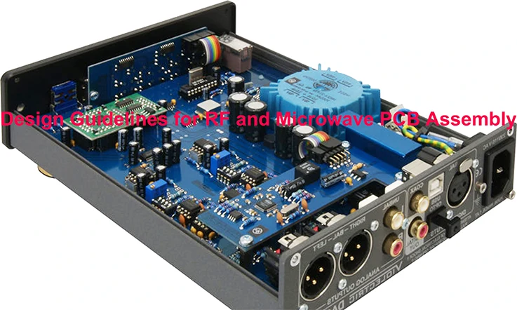
Creating RF and microwave printed circuit boards (PCBs) involves planning. Following specific rules to ensure they can efficiently handle higher frequencies reduce noise and perform effectively. This article delves into design factors. Recommended approaches, for assembling RF and microwave PCBs.
Design Considerations for RF and Microwave PCB Assembly
RF and microwave printed circuit board (PCB) assemblies are components, in electronic devices, such as communication systems, radar systems and test and measurement equipment. Due, to the frequencies and demanding performance requirements of RF and microwave applications careful attention is necessary when designing and assembling PCBs to achieve performance and reliability.
Key Considerations in PCB Design:
Material Selection and Properties: Optimal PCB materials should exhibit low dielectric loss, low moisture absorption, and high thermal conductivity. These characteristics minimize signal degradation and ensure stable performance.
Layer Stackup and Signal Routing: Careful optimization of the layer stackup enables control of impedance and minimization of crosstalk. Dedicated layers for signal routing prevent interference and maintain signal integrity.
Power Distribution and Grounding: A robust power distribution network with low impedance paths is essential to minimize noise and voltage fluctuations. Establishing a solid and continuous ground plane provides a reference potential and reduces electromagnetic interference (EMI).
Trace Width and Spacing: Accurate calculation of trace widths and spacings is necessary to achieve the desired impedance and minimize signal loss. Maintaining proper clearance between traces prevents crosstalk and arcing.
Via Design and Placement: By employing vias with appropriate diameters and aspect ratios, inductance and signal distortion can be minimized. Strategic via placement avoids signal reflections and disruptions.
RF-Specific Considerations:
Matching and Impedance Control: Achieving proper impedance matching between components and transmission lines minimizes signal reflections and maximizes power transfer.
Transmission Line Analysis: Thorough analysis of transmission lines helps determine characteristic impedance, propagation delay, and other parameters. Employing suitable line types and terminations ensures desired signal integrity.
Switching Behavior and Noise Minimization: Considering component switching behavior allows for PCB layout designs that minimize noise generation and propagation. Proper decoupling techniques effectively suppress unwanted signals.
Electromagnetic Interference (EMI) Mitigation: To reduce Electromagnetic Interference (EMI) various methods such, as shielding, filtering and grounding are employed to minimize its impact and adhere to standards.
Microwave-Specific Considerations:
High-Frequency Phenomena and Effects: Proficiency in identifying high-frequency occurrences such as dispersion, skin effect, and dielectric loss is imperative. The optimization of PCB design offsets their influence on signal performance.
Dispersion, Skin Effect, and Dielectric Loss: Apprehending the frequency-dependent attributes of materials is substantial in the engineering of PCBs that curtail signal distortion and degradation.
Advanced Transmission Line Structures: Utilizing advanced transmission line structures like microstrip, stripline, and coplanar waveguide helps achieve desired impedance and signal propagation characteristics.
Microwave Packaging Techniques: Employing microwave packaging techniques, including cavity filters, waveguide transitions, and impedance matching networks, enhances performance and reduces parasitic effects.
Best Practices for Assembly:
Component Selection and Placement: Thoughtful selection of components with appropriate RF/microwave characteristics and careful placement minimize parasitics and optimize performance.
Soldering and Reflow Techniques: Employing controlled soldering and reflow techniques ensures reliable connections and minimizes thermal stress on components.
Testing and Verification: Thorough testing and verification procedures guarantee that the PCB assembly meets performance specifications and industry standards.
By adhering to these design considerations and best practices, engineers can create high-performing and reliable RF and microwave PCB assemblies that meet the stringent requirements of modern electronic devices.
Selecting Substrate Materials for RF/Microwave PCB Assembly
Choosing the substrate material is crucial when designing RF and microwave PCBs as it significantly affects the performance and reliability of the PCB. Hence it’s important to pay attention to selecting the appropriate substrate materials during the design phase. Here are some important factors to consider when evaluating substrate materials:
High Relative Permittivity:
The best materials, for RF and microwave PCBs need to have a permittivity. This feature is crucial because it directly impacts the dimensions and spacing needed for the PCB. Relative permittivity refers to the ratio, between the materials constant and the vacuum permittivity.
Environmental Considerations:
When choosing substrate materials it’s important to consider the conditions. Ensuring temperature stability and determining the lower temperature limits are factors. Opting for substrate materials, with humidity absorption can help uphold the circuit boards performance in high humidity settings.
Thickness of Substrate Materials:
The thickness of the materials used for the substrate plays a role, in avoiding issues like bending of circuit boards, distortion, production delays, higher expenses or electrical breakdown. It’s worth mentioning that materials with thickness per unit area may come at a cost, than thinner alternatives.
Dielectric Loss and Conductor Loss:
The relative permittivity and loss tangent of the substrate materials contribute to the dielectric loss. In high-frequency scenarios, shorter transmission lines can help offset the dielectric loss per unit length, thereby reducing conductor loss. This consideration is crucial for maintaining signal integrity during high-frequency operations.
By carefully considering these factors and selecting appropriate substrate materials, engineers can ensure the reliability and optimal performance of RF and microwave PCBs in various applications.
Summary
Designing and assembling RF and microwave PCBs require meticulous attention to detail and adherence to specific guidelines. By carefully selecting suitable substrate materials, optimizing layer stackup and signal routing, ensuring proper component placement and impedance matching, and implementing effective EMI mitigation techniques, engineers can achieve high-performing and reliable PCB assemblies. Following these design guidelines is crucial for capturing higher frequencies, minimizing noise, and maximizing the overall performance of RF and microwave electronic systems.
At JarnisTech we’re experts, in offering top notch PCB Assembly services backed by than two decades of experience. Our careful PCB assembly procedure follows quality guidelines, such, as ISO 9001;2015 and RoHS compliance. Utilizing PCB design software we assure the delivery of PCB assemblies. Our team of engineers has skills to customize each board accurately according to your unique needs and technical standards.
If you have any inquiries or particular needs concerning PCB assembly services please don’t hesitate to contact us. You can send us an email at [email protected]. Reach out to us by phone at 755/23034656. Our aim is to deliver PCB assembly solutions that go above and beyond what you anticipate.

