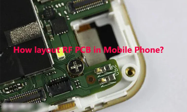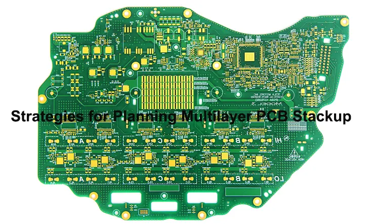
The arrangement of radio frequency printed circuit boards (RF PCBs) is essential, for maintaining notch functionality in smartphones. With the advancements and incorporation of cutting edge technologies like 5G, Wi Fi and Bluetooth in mobile devices the design and setup of RF PCBs have gained more importance. This piece explores the factors and methods used to lay out RF PCBs, in mobile phones to ensure excellent wireless connectivity and performance.
Importance of RF PCB layout in mobile phones
The RF PCB layout holds tremendous significance in mobile phones due to various key reasons:
Signal integrity:
Maintaining optimum signal integrity is paramount in the RF PCB layout to ensure the transmission and reception of high-frequency signals with minimal distortion and loss. Precise implementation of layout techniques such as impedance control and grounding plays a vital role in preserving signal integrity.
Performance:
The effectiveness and operation of a cell phones RF circuitry greatly depend on how the PCB’s arranged. Careful positioning of components and routing of traces can help decrease losses and improve the systems performance.
Battery longevity; The RF circuitry plays a role, in consuming power, in cell phones. By tuning the layout of the RF PCB power usage can be lowered by minimizing losses and increasing efficiency resulting in battery life.
Size and form factor:
The compact size and sleek form factor of mobile phones necessitate efficient utilization of PCB space. Adhering to proper RF PCB layout techniques enables the reduction of RF circuitry’s size and complexity, facilitating more compact and visually appealing designs.
Cost:
A well-designed RF PCB layout contributes to cost reduction in manufacturing by minimizing the required number of layers and components. Furthermore, employing appropriate layout techniques enhances yield rates, thereby mitigating the cost of defective boards.
Regulatory compliance:
Mobile phones need to follow rules that control radio frequency emissions and electromagnetic compatibility (EMC). Having a good RF PCB layout is crucial, for meeting these rules and making sure the device works safely and dependably.
Additionally the RF PCB layout plays a role, in affecting the following areas of phones:
Antenna performance:
The placement and design of the antenna on the PCB exert a substantial influence on its performance, including factors like gain, bandwidth, and efficiency.
Thermal management:
RF components generate heat, necessitating the implementation of proper layout techniques to dissipate heat effectively and prevent thermal damage.
Interference mitigation:
The arrangement of the RF circuit board is essential, for reducing disturbances among parts and systems, within the cellphone.
Because of the importance of RF circuit board layout it is usually assigned to engineers who focus on high frequency design. These experts have a knowledge of RF concepts and mobile phone technology allowing them to carry out the layout accurately and skillfully.
Challenges involved in RF PCB layout
RF PCB layout in mobile phones presents a set of distinctive challenges due to the involvement of high frequencies and the compact size of the devices:
Impedance control:
Ensuring proper impedance matching throughout the RF circuitry is crucial to minimize signal reflections and losses. However, accomplishing this task becomes challenging due to the small size and intricate geometry of mobile phone PCBs.
Grounding and shielding:
Effective grounding and shielding are vital to prevent noise and interference. Nevertheless, achieving optimal grounding and shielding in the context of compact mobile phone designs can be demanding.
Antenna placement:
The exact positioning of the antenna, on the PCB plays a role in how signals are received and sent. Yet locating the spot, for the antenna that meets both visual needs can be quite tricky.
Component placement:
Arranging RF components like power amplifiers and low noise amplifiers with precision is crucial to reduce interference and enhance signal transmission. This becomes challenging because of the space, on mobile phone circuit boards.
Routing:
Meticulous planning of RF trace routing is necessary to minimize losses and preserve signal integrity. The utilization of high frequencies in mobile phones introduces additional complexity to this process.
Simulation and verification:
Thorough simulation and verification of RF PCB layouts are indispensable to ensure compliance with specifications. However, accurately simulating high-frequency RF circuits can be computationally intensive and time-consuming.
Manufacturing constraints:
The compact size and intricate geometry of mobile phone PCBs pose manufacturing challenges. These difficulties can lead to yield issues and increased costs.
Compliance with regulations:
Mobile phone RF PCBs must conform to various regulatory standards, including those governing radio frequency emissions and electromagnetic compatibility (EMC). Meeting these standards adds complexity to the layout process.
Despite these challenges, experienced RF PCB layout engineers can overcome them by leveraging advanced design tools and techniques. By meticulously considering the aforementioned factors, these professionals can develop RF PCBs that meet the stringent requirements of mobile phone applications.
Practices for RF PCB Layout in Mobile Fhone
The skills and methods employed in high-frequency PCB design are as follows:
1. Implementing 45° angles at transmission line corners: This technique reduces back reflection and signal loss, enhancing signal integrity in high-frequency applications.
2. Utilizing high-performance insulation circuit boards: It is essential to select circuit boards with strict control over the dielectric constant. This ensures effective management of the electromagnetic field between insulation materials and adjacent traces, minimizing interference.
3. Enhancing PCB design specifications for high-precision etching: Specifications should include managing total line width errors within a tight tolerance, controlling undercut and cross-sections of traces, and specifying plating conditions for sidewall coating. These measures address the skin effect issue associated with microwave frequencies and enable the achievement of high-performance specifications.
4. Minimizing lead inductance: In high-frequency environments, it is advisable to avoid components with lead wires. Surface mount components are preferred to mitigate the tap inductance caused by protruding leads.
5. Careful consideration of signal vias: It is important to avoid using plated through-hole (PTH) vias on sensitive boards, as they introduce additional lead inductance. Alternative via methods should be employed to maintain signal integrity.
6. Incorporating an extensive ground plane: Multiple ground planes should be included and connected using stitched vias to minimize the impact of three-dimensional electromagnetic fields on the PCB. This facilitates effective grounding and reduces noise.
7. Selecting appropriate plating processes: Non-electrolytic nickel plating or gold immersion plating is preferred over the hot air solder leveling (HASL) method. These plating processes improve high-frequency current distribution and provide better skin effect. Additionally, the use of high solderability coatings reduces the number of leads, contributing to reduced environmental pollution.
8. Managing solder mask application: Solder mask prevents solder paste from flowing, but its application across the entire board surface can introduce changes in electromagnetic energy in microstrip designs due to thickness variations and unknown insulating properties. Instead, solder dams are commonly used in high-frequency designs to manage the transition from microstrip to coaxial cable. This approach considers the edge effects in microstrip designs, minimizes back reflections, and reduces noise and signal interference.
By applying these skills and methods, high-frequency PCB designers can optimize signal integrity, reduce noise, and enhance the overall performance of circuits operating at microwave frequencies.
Tools and Techniques for RF PCB Layout
Tools for RF PCB Layout:
1. Computer-Aided Design (CAD) Software: Specialized software such as Altium Designer, Cadence Allegro, and Mentor Graphics Xpedition are commonly used for designing and simulating RF PCBs.
2. Electromagnetic (EM) Simulation Software: Tools like Ansys HFSS, CST Microwave Studio, and Sonnet Suites enable engineers to simulate the electrical and electromagnetic behavior of RF PCBs, helping optimize performance and identify potential issues.
3. Vector Network Analyzers (VNAs): VNAs are essential instruments for measuring and characterizing RF circuits. They allow engineers to measure impedance, gain, return loss, and other important parameters.
4. Spectrum Analyzers: Commonly utilized for examining the frequency spectrum of RF signals aiding engineers in detecting and resolving interference, noise and various signal integrity challenges.
5. Signal Generators: Signal generators produce RF signals for testing and characterization purposes, enabling engineers to verify circuit behavior and performance.
Techniques for RF PCB Layout:
1. Impedance Control: Maintaining consistent impedance throughout RF traces is crucial. Engineers use impedance calculators, simulation tools, and matching techniques to achieve proper impedance control.
2. Grounding and Shielding: Establishing a solid ground plane, employing multiple ground layers, and incorporating shielding enclosures help minimize noise, interference, and signal degradation.
3. Component Placement: Optimizing the placement of RF components is important for minimizing signal loss, interference, and thermal issues. Strategic component positioning can enhance overall performance.
4. Routing: RF traces should be routed with smooth bends, proper spacing, and differential routing techniques to ensure signal integrity, minimize crosstalk, and reduce losses.
5. Simulation and Verification: EM simulation tools are used to verify the performance of the layout before fabrication. Measurements and testing are conducted to ensure compliance with specifications and desired performance.
6. Optimization: Various layout techniques are employed to minimize losses, improve signal integrity, and enhance overall RF circuit performance.
7. Manufacturing Considerations: Designing for manufacturability is crucial. Engineers consider trace width and spacing limitations, fabrication tolerances, and other manufacturing constraints during the layout process.
8. Ensuring adherence, to industry standards and regulations is crucial for RF PCB layouts, including compliance with guidelines established by organizations, like the FCC and ETSI.
Advanced Techniques:
1. Using layers, in PCB design, known as multilayer stackups is beneficial for optimizing signal routing and controlling impedance effectively.
2. The inclusion of components like capacitors and inductors within PCB layers referred to as embedded passives helps save space and boosts performance.
3. Differential signaling techniques enhance noise immunity and signal integrity in high speed applications.
4. Designing transmission lines with impedance values ensures proper matching with connected components. A process known as controlled impedance transmission lines.
5. Techniques such as impedance matching, skew control and crosstalk mitigation play a role, in facilitating high speed digital signal routing for performance.
By utilizing these strategies and methods RF PCB layout engineers can craft notch dependable RF PCBs capable of delivering high performance across a variety of applications.
Conclusion
The arrangement of RF PCBs, in smartphones is an crucial procedure that significantly affects functionality. Through positioning of components routing high frequency traces isolating ground planes implementing RF shielding and employing impedance matching methods smartphone makers can improve RF performance boost signal integrity and provide users with wireless connectivity. As wireless technologies advance the significance of RF PCB layout, in smartphones rises, facilitating communication and an improved mobile user experience.


