
Signal integrity has become an increasingly critical aspect to consider when developing circuits and PCBs, especially for high-speed processor designs. With frequencies inside digital circuits increasing, even short connections can function as transmission lines, which can potentially impact signal integrity.
Even digital signals can be affected by analog phenomena that can ultimately disrupt circuit functionality. Therefore, it is imperative to prioritize maintaining signal integrity during the circuit design phase by incorporating design simulations and tests. Without proper signal integrity engineering during the design process, it can be challenging to make modifications once the board has been finalized.
To address this issue, top-notch PCB design software packages offer signal integrity engineering and checking capabilities. Utilizing such tools can ensure that designers can conduct timely and effective checks during the development of the design. As a result, designers can optimize PCB layout to achieve correct signal integrity engineering while minimizing issues that may arise once the PCB is constructed. The optimization of PCB layout is crucial to ensure the effective operation of the circuit.
What Is Signal Integrity In a PCB ?
Signal integrity refers to a set of crucial activities performed during the design, analysis, and verification of a PCB to maintain the integrity of the electrical signals that flow along its traces. This includes ensuring the voltage and current values, as well as their trends over time, are preserved. With the prevalence of high-frequency digital circuits utilizing transmission lines, noise and interference easily disrupt signal integrity, making it a critical aspect of circuit design.
To prevent signal distortion in digital circuits with fast rising or falling edges on the order of tens of picoseconds, the PCB traces must be appropriately designed to ensure high bandwidth and avoid modifying spectral components of the signal. Rapid edge transitions in signals are among the major sources of crosstalk and demand careful consideration.
While signal integrity was previously only vital to specific applications like military, aviation, telco, and medical systems, it is now standard for electronic circuits using highly integrated digital components such as microprocessors, FPGAs, SoCs, high-speed buses, and DDR memory. PCB design engineers must prioritize signal integrity in their design process to ensure the circuits operate as intended at high speeds and under the influence of external noise.
Introduction to PCB Signal Integrity
PCB signal integrity refers to the ability of a printed circuit board (PCB) to reliably and accurately transfer electrical signals between different components and devices. Signal integrity issues can arise due to factors such as high-frequency switching, signal reflection, crosstalk, and electromagnetic interference (EMI). Ensuring good signal integrity is crucial in high-speed digital and analog circuits to avoid signal distortions and errors. This requires careful consideration of PCB design and layout techniques, use of high-quality components, and proper testing and validation procedures.
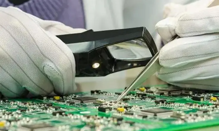
Signal Integrity Testing and Validation
Signal integrity testing and validation involve measuring and verifying the performance of a PCB or system to ensure that it meets the required specifications. Here are some common signal integrity testing and validation techniques:
● Time-domain analysis: Time-domain analysis, such as eye diagram measurements, can help identify timing errors, jitter, and other problems. The quality of the signal can be analyzed by measuring the rise and fall times, important for maintaining good signal integrity at high speeds.
● Frequency-domain analysis: Frequency-domain analysis, such as spectrum analysis or Fourier transform, can verify the frequency content of the signal and check for unwanted harmonics.
● Return loss and impedance measurements: These measurements can help identify impedance mismatches and signal reflection at various points in the circuit.
● Crosstalk analysis: Crosstalk analysis can identify the level of crosstalk generated between traces and signal integrity degradation caused by them.
● Electromagnetic interference (EMI) testing: EMI testing can determine the level of electromagnetic radiation emitted by the system, and comply with regulatory agency standards.
● Signal integrity simulation verification: Comparing the results of signal integrity simulation with actual measurements helps verify the simulation accuracy, and optimize the design for performance.
By performing these signal integrity testing and validation techniques, designers can verify the performance and functionality of their PCB or system, and identify any shortcomings they need to correct.
Design Guidelines and Best Practices for PCB Signal Integrity
Design guidelines and best practices for PCB signal integrity focus on maintaining good signal quality and reducing the impact of parasitic effects. Below are some common guidelines and best practices:
● Proper layer stackup: Use an appropriate layer stackup that includes ground and power planes, signal layers, and adequate insulation to achieve controlled impedance, minimize crosstalk and EMI.
● Keep signal paths short and direct: Keep the lengths of signal paths as short and direct as possible, to reduce the chances of distortion, loss, and crosstalk. The length of differential pairs should be matched to maintain the characteristic impedance.
● Proper grounding techniques: Use effective grounding techniques and dedicated return paths to achieve a low impedance and reduce the ground bounce and EMI. Consider using a split ground plane to help isolate noisy circuitry from the ground reference.
● Proper Power distribution: Ensure an adequate power distribution network with minimal inductance and resistance to avoid voltage fluctuations and noise.
● Use decoupling capacitors correctly: Strategically place decoupling capacitors as close as possible to active components to reduce the power supply noise.
● Proper termination: Use proper termination techniques such as a series resistor or parallel termination at the receiving end of signals, to prevent reflections and avoid signal distortion.
● Signal integrity simulation: Perform signal integrity simulations to optimize the PCB performance and identify issues with electronic design automation (EDA) tools.
By following these guidelines and best practices, PCB designers can reduce the impact of parasitics on signal quality, reduce the likelihood of errors during signal propagation, and optimize the circuitry for good signal integrity.
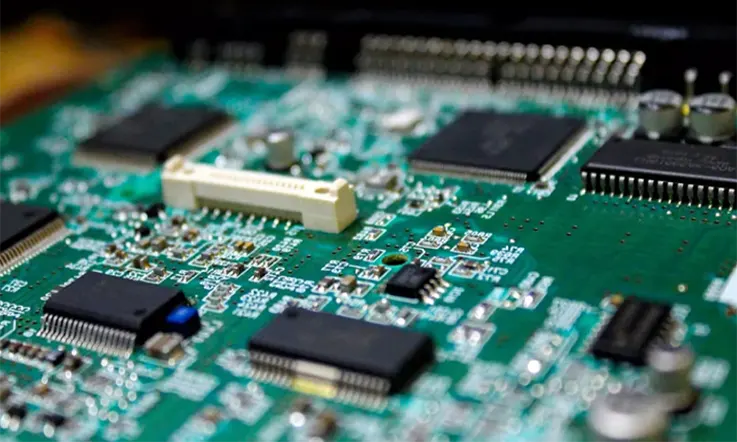
Parasitic Effects and PCB Design Considerations
Parasitic effects refer to the unintended and undesirable behavior of certain electrical components or structures on a printed circuit board (PCB). These effects can cause signal degradation, noise, and even complete failure of a high-speed circuit. Some common parasitic effects include capacitance, inductance, resistance, and electromagnetic interference (EMI).
To minimize the impact of parasitic effects, PCB designers must consider certain design practices and techniques. Here are some considerations:
● Proper PCB layout: Circuit layout can significantly impact the parasitic effects on a PCB. This includes careful consideration of component placement, signal routing, and power routing.
● Ground planes: Proper grounding techniques such as the use of ground planes can help minimize EMI and other parasitic effects and distribute power evenly across the PCB.
● Decoupling capacitors: Proper use of decoupling capacitors helps to reduce voltage fluctuations in the power supply network, which can cause noise and signal distortions.
● Controlled impedance routing: Controlled impedance routing helps maintain consistent signal integrity by matching the impedance of traces to components.
● Crosstalk prevention: There are several techniques to prevent crosstalk, such as minimizing the distance between tracks, using shielded traces, and avoiding parallel runs.
By considering these factors and other design best practices, designers can minimize parasitic effects and improve the signal integrity of their high-speed circuits.
Use Signal integrity Simulation Tools and Techniques in PCB Design
Signal integrity simulation tools and techniques can help engineers analyze and optimize a PCB design to ensure good signal quality and performance. Here are some common signal integrity simulation tools and techniques:
● Time-domain simulations: Tools such as SPICE (Simulation Program with Integrated Circuit Emphasis) can simulate the behavior of electrical signals over time to identify possible signal degradation or distortions. It can also analyze noise, crosstalk, and other effects on signal quality.
● Frequency-domain simulations: Frequency-domain simulations, such as those done using a network analyzer, can identify unwanted harmonics, resonances, and other frequency-related issues in the circuit.
● Electromagnetic field simulators: Simulators, such as ANSYS HFSS (High-Frequency Structural Simulator), provide a more detailed simulation of signal propagation and electromagnetic interference. These tools can help predict the characteristics of a signal as it travels through a circuit and analyze the effects of parasitics, electromagnetic interference, and other factors on signal quality.
● Eye diagram analysis: Eye diagram analysis can provide a visual display of signal quality and help identify timing errors, jitter, and other problems. Tools like MATLAB and Python can be used for eye diagram analysis.
● Time-domain reflectometry (TDR): TDR can help diagnose transmission line issues such as impedance mismatch, reflection, and propagation delay.
By leveraging these simulation tools and techniques, designers can quickly and effectively analyze and optimize their PCB design for signal integrity.
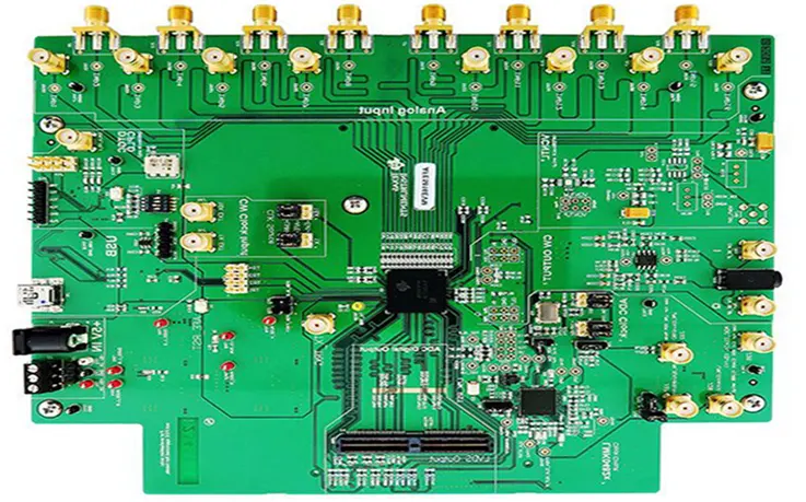
Factors Affecting Circuit Board Signal Integrity
In PCB design, faster signal rise times are likely the most significant factor that leads to signal integrity issues. While low to moderate frequency circuits and devices with modest signal rise and fall times may not experience problems caused by PCB design, working with high frequencies, such as RF and beyond, results in significantly shorter signal rise times. This makes signal integrity degradation owing to PCB design a critical issue that demands attention.
Various factors contribute to signal integrity degradation, and PCB design engineers need to consider them carefully. These contributing factors include:
● Transmission Line Effects: As the length of traces on the PCB approaches or exceeds the wavelength of signals being transmitted, they begin to function as transmission lines.
● Reflections: When signals encounter discontinuities in the transmission line (such as open or shorted stubs), they reflect back down the line, causing signal degradation.
● Cross-Talk: When two traces run in close proximity, they can cause electromagnetic interference that degrades signal quality.
● Ground Bounce: The switching of digital signals causes transient currents to flow through the ground network, creating spikes and noise.
● Power Integrity: Insufficient power and ground distribution on the PCB can cause voltage variations that result in signal degradation.
Designers must carefully consider each of these factors when designing PCBs for circuits that demand optimal signal integrity and high frequencies to ensure circuits operate as intended with effective signal integrity.
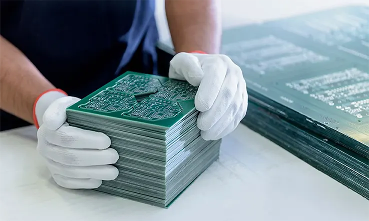
Signal Integrity in PCB Manufacturing
Signal integrity in high-speed transmission strongly depends on how designers route transmission lines, beginning with careful placement of components. To achieve this, the circuit board’s functional sections should be identified and components arranged in a way that provides the quickest and most direct signal routes possible for high-speed circuits. An effective approach to this process involves establishing an optimal board layer stackup to facilitate impedance routing effectively.
PCB designers must work closely with manufacturers to determine the board layer count and configuration, ensuring that the circuit board is not only optimized for signal integrity but also manufacturability and its working environment. At JarnisTech, we collaborate with clients to create circuit boards that not only offer superior high-speed performance but are also cost-effective to produce. Our expertise lies in guiding clients through the design and manufacturing process, resulting in PCBs with optimal signal integrity, durability, and reliability.
Signal Integrity: How to Achieve ?
Signal integrity is a crucial aspect that PCB designers must keep in mind from the outset of drafting the schematic until the final test of the board. To ensure signal integrity is retained, designers must consider restrictions on trace length and carefully select connectors.
After finishing the schematic, the designer moves on to PCB layout, adhering to limitations set by standards for different types of connectivity. For example, the USB2.0 standard necessitates 90-ohm differential impedance for traces. The layout designer selects an appropriate stack-up and sets up rules specifying allowed layers for particular traces and their geometry, among other factors.
Upon completing the layout, it is advisable to run computer simulations that verify whether the circuit board is compliant with standards. Despite many existing standards, they do not offer guidance on competing signals, ground plane breaks or other issues that arise in practical PCB design. Hence, simulating the routed board is imperative to verify that crucial high-speed traces conform to the standard. This simulation technique is known as Signal Integrity Analysis, where designers can examine critical issues affecting signal degradation, crosstalk, and other factors that can impact overall signal quality.
Signal integrity: How to Improve ?
● Stack-up Definition: In PCB design, the selection and arrangement of layers must balance cost, size, and signal integrity. To achieve good impedance control, it is crucial to insert power and ground planes that offer a return path to ground for every signal, optimally evenly spread in the stackup. This approach guarantees close proximity between each signal layer and one of the planes, ensuring an uninterrupted signal flow.
Moreover, employing the right materials is equally important. The thickness of the copper, dielectric, and their respective constants all significantly impact circuit performance. Designing high-speed circuits with common FR-4 materials may not be optimal. Instead, choosing materials with low dielectric constants (Dk) can help mitigate signal distortions and phase changes. One such example is Rogers laminates, particularly Rogers RO4350, which offer unique properties for high frequencies. Although more expensive than FR-4, materials like these hold a clear advantage for high-speed PCB design.
PCB design engineers must carefully assess material choices, balancing cost, performance, and long-term circuit reliability to deliver high-quality, effective PCB designs.
● Impedance Control: Impedance control is crucial in PCB design, and achieving optimal coupling between the size and position of PCB traces and substrate characteristics is key to maintaining signal strength within predetermined parameters. Good coupling ensures signal strength increases, while poor coupling results in power losses and signal degradation.
To ensure a good impedance coupling, PCB traces must have uniform shape to guarantee a constant dielectric constant along the trace. Designers can adjust track width and consult specialized calculators available online to check the impedance value. Poor enforcement of these criteria can result in signal reflections and wave interference, reducing the signal strength and affecting its transmission.
In multilayer PCBs, it is crucial to pay attention to impedance changes, especially when a trace on one layer with a different impedance must continue on an adjacent layer with a different impedance, resulting in signal reflections. Maintaining impedance control requires designers to ensure that the impedance remains constant along the entire trace, even as they move across multiple layers. This attention to detail ensures effective impedance control, mitigating power losses and signal degradation, resulting in high-quality, reliable PCB designs.
● PCB Layout: Ensuring sufficient signal integrity is crucial, mainly for traces carrying high-speed signals in PCB design. Designers need to pay particular attention to the signal paths between the origin and destination, as well as the paths back to ground. Certain guidelines help achieve efficient signal routing:
● Avoid right angles on traces, as they increase parasitic capacitance and result in impedance fluctuations and signal reflections. Instead, choose a gentle angle of 45 degrees or curved parts for better signal integrity.
● Via holes should be used cautiously as they increase traces’ length and induce parasitic inductance and capacitance.
● Separate high-speed signals from low-speed signals or routing them perpendicular on neighboring layers to reduce crosstalk.
● Separate digital signals from analog, as digital signals produce harsh square waves, inducing noise in the analog signals and causing lower signal integrity.
By following these guidelines, designers can optimize signal integrity while reducing noise levels and interference, ultimately leading to high-quality, reliable PCB designs.
● Crosstalk: Crosstalk is an unwanted coupling between adjacent traces on a PCB, resulting from either inductance or capacitance. In high-speed transmissions, crosstalk can severely degrade signal quality and is often challenging to predict or replicate. This difficulty arises due to high-speed signals traveling at very high frequencies.
Designers can address the issue by ensuring adequate spacing between high-frequency or high-speed traces, perhaps utilizing any excess space for less critical traces. This approach offers an immediate benefit because the coupling effects decrease inversely proportional to the square of the distance between the tracks, making it a suitable method to mitigate crosstalk.
By increasing the spacing between high-speed signals, designers can minimize the adverse effects of crosstalk and maintain signal integrity. This technique is an essential component of PCB design and can ultimately optimize circuit performance.
Future Trends and Challenges in PCB Signal Integrity
As electronic systems continue to advance and evolve, there will be several future trends and challenges in PCB signal integrity. Here are some of them:
● Increasing use of high-speed serial interfaces: With the increasing demand for data transmission, high-speed serial interfaces such as PCIe, USB, and Ethernet are becoming more prevalent, driving higher data rates and requiring more rigorous signal integrity design.
● Increasing complexity of systems: The complexity of electronic systems is increasing due to the integration of multiple functions on a single PCB. This complexity makes it more challenging to maintain good signal integrity.
● Incorporation of digital signal processing techniques: The incorporation of digital signal processing techniques such as filtering and equalization expects to correct signal distortions and improve signal quality, leading to an improved signal-to-noise ratio.
● Shrinking form factors: The trend toward smaller form factors and higher pin densities puts additional demands on signal integrity, including increased crosstalk and noise.
● Increasing use of wireless connectivity: The proliferation of wireless communication in electronic systems, such as Bluetooth and Wi-Fi, raises new challenges for signal integrity, as the design must account for both the wired and wireless aspects of the system.
● Higher frequency operation: To meet the bandwidth requirements, PCB designers must design for higher frequencies, making it difficult to manage the signal integrity.
To address these challenges, PCB designers must continue to follow best practices, such as circuit simulation, research of new materials with more predictable performance, and constant adaptation with EDA tools to meet new signal integrity issues. They must also stay up-to-date with emerging technologies and standards.
Summary
Our company is a leading PCB manufacturer based in China, offering comprehensive PCB production and assembly services. We specialize in delivering high-speed and high-frequency PCBs and possess the technical knowledge and experience to utilize advanced signal integrity simulation tools that help develop PCBs that meet the highest standards of quality.
At JarnisTech, we are committed to providing our clients with exceptional service and products, and our engineering expertise is unmatched. We are dedicated to working alongside our clients, ensuring that their high-speed PCB assembly meets their unique specifications and requirements. As a leading PCB manufacturer, we prioritize staying up-to-date with industry advancements and invest in cutting-edge solutions to enhance our production process and deliver optimal outcomes.
If you are looking for a contract manufacturer with the expertise to deliver the highest quality high-speed PCB assembly, look no further than JarnisTech. Our team is eager to collaborate with you on your next project and provide you with comprehensive information on our capabilities and services. Please reach out to us today to learn more.


