The Electronic Design Automation (EDA) market segment encompasses specialized software, hardware, and services geared towards supporting the complete lifecycle of semiconductor device manufacturing. This includes aiding in the definition, planning, design, implementation, verification, and final manufacturing of these devices, also referred to as “chips.”
The primary service providers in the semiconductor manufacturing space are semiconductor foundries, also known as fabs. These facilities are highly intricate and demand significant investment, and may be owned and operated by large vertically integrated semiconductor companies or independent “pure-play” manufacturing service providers. The independent model has emerged as the dominant business approach in the semiconductor manufacturing space in recent years.
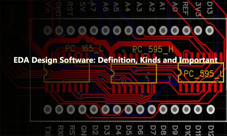
What Is EDA?
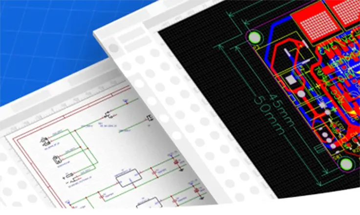
EDA stands for Electronic Design Automation, which is a process of using computer and professional software tools to design, develop, analyze, verify, and produce electronic systems at the chip and circuit board levels. EDA uses automation technology to improve design efficiency and reliability, and help engineers to quickly complete the design, verification, and production of electronic products. EDA encompasses a variety of tools and techniques, including circuit simulation, layout design, timing analysis, logic synthesis, and FPGA design.
An EDA involves a group of software tools and programming systems that enhance the efficiency, accuracy, and ease of the design process for electronic systems. Beyond integrated circuits, EDA can be applied in the design of PCBs and other electronic components.
In a word, EDA is a critical tool for modern electronic design, serving as a powerful electronic computer-aided design (ECAD) resource for designers looking to create complex electronic systems using cutting-edge software tools.
How Does EDA Work?
Electronic Design Automation (EDA) is primarily a software business that enables the design and manufacture of chips through the use of sophisticated and complex software programs. These software programs function in three primary ways:
1.Simulation tools
Simulation tools that predict the behavior of proposed circuits, design tools that assemble and connect circuit elements, and verification tools that examine the logical or physical representation of the chip to check for correct connections and required performance.
2.Design Tools
Design tools are utilized to create a collection of circuit elements that implement a proposed circuit function, by both a logical and physical process. The logical process involves assembling and connecting said circuit elements while the physical process pertains to the development of interconnected geometric shapes that will construct the circuit during manufacturing. These tools are provided through a blend of fully automated and interactively guided features.
3.Verification Tools
Verification tools are essential software applications used in Electronic Design Automation (EDA) to examine the logical or physical representation of semiconductor chips to confirm that the design is connected correctly and delivers the required performance.
While EDA products are mostly software-based, in some situations, physical hardware is also used to deliver capabilities. This occurs when extremely high performance is necessary, such as during simulation and verification of large amounts of data. Dedicated hardware models of the circuit typically perform far faster than software programs that simulate the same model, making hardware delivery critical for completing various tasks within reasonable time frames (hours to days versus weeks to months). Emulation and rapid prototyping are the two main delivery mechanisms for EDA hardware.
The Development History of EDA
EDA has a history dating back to the 1950s when programmers used low-level programming languages to design digital computer systems. In the 1960s, the first tools specifically for digital circuit design appeared, such as bit-width analysis, logic synthesis, and simulation tools. In the 1970s, EDA began to enter the field of analog circuit design, including PCB and integrated circuit design.
In the 1980s, EDA became increasingly popular, and users from various fields, such as computer and communication systems, embedded systems, automotive and medical devices started to widely use it. Subsequently, EDA began to develop towards computer cloud technology, and many EDA tools were ported to cloud platforms, allowing users to use them through cloud services. Currently, EDA technology has become the core of electronic system design and has made important contributions to the development of modern high-tech industries.
The Role and Significance of EDA
EDA(Electronic Design Automation)technology forms the basis for the comprehensive development of electronic system design tools. Its significance and role include:
●Shortened development time: EDA tools accelerate the design process, reducing the time required for product development, allowing companies to bring products to market more quickly.
●Improved design efficiency: The automation features of EDA tools reduce errors, minimize repeated tasks, reduce manual workloads, and provide real-time error checking during the design process, thereby improving design efficiency.
●Improved design quality: EDA tools reduce human error and improve the accuracy of circuit routing, thereby improving the quality and reliability of the design.
●Cost reduction: EDA tools and technology can lower development costs, reduce failure rates on the production line, and lower material costs.
●Promotion of innovation: EDA tools provide numerous analysis and simulation tools, enabling designers to experiment with multiple designs and explore multiple solutions more quickly, promoting innovation in new technologies, products, and markets.
In a word, EDA technology plays a crucial role in modern electronic system design, serving as a necessary tool to enhance productivity and innovation capabilities.
Classification of EDA Software
EDA software can typically be classified into the following:
●Circuit Simulation Software: Used for analyzing and verifying circuit behavior and performance, including voltage, current, and signal transmission.
●Layout Design Software: Used for creating and editing physical layouts of PCBs, ICs, and other circuit designs.
●Logic Synthesis Software: Converts logic code in high-level hardware description languages (HDL) into circuits.
●Timing Analysis Software: Analyzes timing requirements to identify timing conflicts or optimize timing paths.
●Low Power Design Software: Used for analyzing and optimizing circuit power consumption in systems.
●FPGA Design Software: Supports the design of programmable logic devices (FPGA), including system-level design, IP cores, synthesis, layout, and routing.
●Physical Verification Software: Used for verifying physical characteristics of circuits, such as compliance of layout with specifications and signal integrity.
In addition, some EDA software implements multiple functions, such as software that integrates layout design and physical verification, as well as software that supports both FPGA and ASIC design.
Comparison of Common EDA Software
There are many common EDA software options available, and here are some of the comparisons of their features and characteristics:
●Cadence: Primarily focused on IC design, supports a variety of SIP design and test flows, including IC design, layout design, silicon validation, and system-level design.
●Mentor Graphics: Offers a variety of EDA tools, including widely-used tools in simulation, RTL synthesis, layout design, and ultimate source automatic routing (UGC).
●Synopsys: Synopsys products include integrated circuit and system-level design, silicon validation and design optimization, as well as software security and quality testing. Additionally, it also covers tools for automation, layout, and physical verification.
●Altium Designer: Provides a comprehensive one-stop solution for PCB and electronic product design, supporting the entire process from prototype design to production manufacturing.
●Proteus: Mainly used for simulation and circuit design of modular electronic circuits, with the characteristic of being easy to use.
●KiCAD: It is a highly recommended EDA tool for PCB design and circuit simulation, boasting several advantageous features. As open-source software, it is available for free, including the code, and offers a comprehensive range of capabilities typically found in proprietary tools. One example is its 3D viewer, which enables interactive canvas inspection of PCB board layouts, along with a Gerber file generator, artworks, an extensive library, and a bill-of-materials generation system. Another substantial benefit of KiCAD is that there are no limitations in terms of size or layers.
●Autodesk Eagle represents an inexpensive option in PCB design software that is tailor-made for beginners. The acronym stands for “Easily Applicable Graphical Layout Editor.” With Fusion 360 software from Autodesk, the tool provides additional electrical and mechanical features to enable a detailed analysis and verification of designs. Eagle has a multi-window GUI with several automation features that simplify the design process, including auto-routing, task scripting, design check, electrical rule checking, and more.
●Pulsonix, a product by UK-based company WestDev, is an advanced PCB design tool exclusively available for the Windows platform. Its intuitive interface and diverse range of capabilities are particularly noteworthy. Among its advanced PCB design features are flexi-rigid design, chip-on-board, embeddable components on PCB layers, definable snapping tolerance for accurate component placement, advanced selection mask browser, and dynamic copper pour to automatically repair damaged copper areas.
●EasyEDA is a web-based PCB design platform that eliminates the need for offline setup or installation. The online platform offers a complete range of capabilities that can be found in paid PCB design tools. These capabilities include instant schematic capture from various file formats, layout design, circuit routing, auto-routing, library creation and management, and cloud-based team collaboration and project management tools.
●DipTrace PCB Designer is a software solution intended primarily for those who need to create schematic diagrams and PCB layouts. The application consists of four sub-modules, namely the Schematic Capture Editor, Component Editor, Pattern Editor, and PCB Layout Editor.
●SolidWorks PCB is a highly productive tool that efficiently combines ECAD (electronic computer-aided design) and MCAD (mechanical computer-aided design) for seamless integration of electro-mechanical components with PCB layout. The software’s advanced capabilities enable designers to work with electronic, mechanical, and embedded software designs in a single environment, thereby optimizing the design process and reducing time to market.
It is necessary to choose the appropriate EDA tool according to specific needs or projects. These tools have their unique functions, suitable for different circuit design and development tasks, and can significantly improve the efficiency and quality of electronic product development.
EDA Tool Tips That Will Make You a Successful PCB Designer
Conducting thorough research on EDA tool vendors and selecting a vendor with a track record of success is a worthwhile practice. This may allow for efficient initiation of work processes with the provision of dependable tools. To clarify doubts or inquiries, one should not hesitate to contact the support line or participate in user groups. These available resources can aid in understanding the tools thoroughly, thus optimizing system performance.
Numerous EDA tool vendors are available; however, Cadence is a reputable and established option. With extensive experience in providing the highest level of technology in PCB design systems, Cadence has a comprehensive understanding of the requisites of PCB designers such as yourself. Their high-level OrCAD PCB Designer features diverse and advanced design tools that are essential in producing optimal results.
Applications of EDA
(Electronic Design Automation) technology is widely used in the design, validation, and production of various circuit boards and chips, as well as the development and testing of electronic systems and devices. Here are some applications of EDA:
●Integrated Circuit Design (IC Design): Designing and manufacturing integrated circuits, including digital and analog ICs, microprocessors, memories, and microcontrollers.
●Printed Circuit Board Design (PCB Design): Designing and manufacturing PCB boards, including analog and digital signal boards, high-frequency, and RF boards, high-speed transmission boards, etc.
●Internet of Things (IoT): Developing and designing embedded systems, embedded sensor IoT nodes, embedded wireless communications, IoT cloud services, etc.
●Automotive electronics: Designing vehicle electronic systems, including vehicle electrical, control systems, in-vehicle entertainment, and autonomous driving, etc.
●Communication systems: Designing and developing communication system components, including wireless gateways, modems, digital signal processing, and optical transmission components.
●Medical devices: Designing and developing various medical devices, including medical image and signal recognition systems, medical electronic therapy devices, electroencephalography (EEG), electrocardiography (ECG), and X-rays, etc.
In short, EDA technology plays an important role in the design, manufacturing, and testing of modern electronic systems and devices, and supports the development of numerous application areas with its advanced functions and performance.
Roles of EDA in IC design
In chip design, EDA plays an instrumental role in mitigating risks and minimizing costs associated with trial and error. Since most chip products cannot be altered after manufacturing, and their designs are both complex and costly, EDA serves at least three fundamental purposes in the design process.
●Firstly, EDA tools are capable of converting complicated physical problems into quantitative models, simulate circuit processes in virtual software, and replicate various effects during chip development, thereby allowing designers to quickly identify potential design defects and mitigate risks.
●Secondly, EDA tools enable designers to simulate and analyze optimal solutions for various performance, power consumption, cost, and other conditions while ensuring proper logic functionality. Solving multi-objective constraint problems is critical for designing chips that meet various operational requirements and reducing trial and error costs.
●Thirdly, EDA tools enable the verification of model consistency, ensuring that the logic functions of the chip remain consistent throughout multiple design stages. Overall, EDA serves as a fundamental underpinning in chip design, enabling rapid identification and resolution of design risks while promoting optimal chip performance, lower costs, and higher design efficiency.
Therefore, Why EDA is so Important In Integrated Circuit design and Manufacturing?
Semiconductor chips have evolved to become incredibly intricate structures that are composed of a vast number of circuit elements, and interactions between these elements can be subtle or complex. Furthermore, the manufacturing process variations can result in even more complicated interactions and behavioral changes. Without sophisticated automation, managing this level of complexity would be nearly impossible. EDA tools are essential to address this issue by providing advanced technology that manages the entire chip design and manufacturing process, enabling efficient design workflows and addressing the inherent complexity of chip development.
It should also be emphasized that errors in a manufactured chip can be catastrophic, leading to an entire project’s failure. Unlike software, which can be updated or patched, chips are permanent, and any error in design or manufacturing will have permanent consequences. Therefore, it is essential to design and manufacture chips with the utmost accuracy and precision, which can only be achieved through the use of EDA tools.
Overall, EDA technology plays a vital role in the modern chip industry, enabling efficient management of chip complexity and eliminating the cost, time, and resource drain incurred by frequent errors and shortcomings that inevitably arise in the absence of automation. By providing powerful EDA capability, design accuracy and reliability are optimized, and a company’s risk profile is minimized, ensuring business success and maximizing customer satisfaction.
Final Words
EDA tools serve as the backbone of the integrated circuit design and manufacturing process, as well as the vehicle for integrated circuit design methodologies. They act as the linkage and bridge between the design and manufacturing phases. To complete the design process and manufacture integrated circuits, PCB Layout designers need to leverage EDA tools. Given the escalating complexity of chip design, integrated circuits leveraging advanced process nodes can host billions of semiconductor devices. As the design complexity scales up, chip design without utilizing EDA is no longer feasible.
Now, the domain of chip design has shifted to cover system design, which entails that the complexity of these devices encompasses an entire system that requires substantial software components. To meet the needs of this broader definition of EDA, several EDA vendors now offer world-class products that cater to the development of secure, high-quality, and highly compliant software. These software solutions aim to address the increased complexity of integrated software systems, providing a comprehensive toolkit for efficient and effective software development in the broader context of integrated system design.
Related Posts:
1. Everything You Should to Know on Altium PCB Design Software
2. Which One Are the Best Auto-route PCB Software?
3. PCB Traces: The Critical Role of Traces in PCB Design and Manufacturing
4. ExpressPCB Design Tool: A Comprehensive Guide to Using ExpressPCB
5. Avoid These 5 Common PCB Design Mistakes
6. You Need to know the PCB Design Software: Eagle PCB
7. Kicad PCB: How to Understand It?
8. What Is the Difference Between Altium and Eagle?
9. How to Make a Arduino PCB – You Must to know Everything About It
10. PCB Design Tips