
The routing of traces on a printed circuit board (PCB) is a critical step in the layout process, enabling the required functionality and connectivity for the board. Manual routing can be extremely time-consuming, underscoring the importance of advanced autorouting capabilities in PCB design software. For complex PCBs, it is essential to leverage routing tools and algorithms that automate portions of the routing process while still allowing the designer precise control over the results.
Advanced PCB design software offer intelligent autorouters utilizing sophisticated pattern matching and trace negotiation abilities to significantly reduce routing time. Constraint management and design rule checks further automate the process by guiding the autorouter based on the unique requirements of the design. However, human oversight remains important, as the designer must define routing priorities, review results, and manually route critical nets. Leveraging both advanced autorouting capabilities and human insight allows for an optimal PCB routing workflow that balances automation with precision, ensuring maximum efficiency in creating a high-quality routed layout.
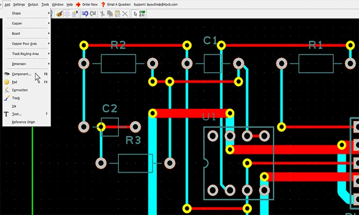
What is PCB Routing?
PCB routing refers to the process of designing the copper traces on a printed circuit board (PCB) that will electrically connect the various components on the board. The main goals of PCB routing are:
Connect components according to the schematic – All components that are connected on the schematic need traces between them on the PCB.
Minimize trace length – Shorter traces mean better performance by reducing resistance and inductance. This improves speed and power efficiency.
Avoid collisions – Traces must not overlap or run into components and other traces. Proper clearances must be maintained.
Meet trace width requirements – Traces must be wide enough to carry the required amount of current. Thicker traces are needed for higher currents.
Maintain impedance control – For high speed signals, trace widths and distances from ground planes must be controlled to match impedance requirements.
Follow board constraints – Traces must be routed within the board layers and comply with manufacturability rules.
Routing is done with PCB design software that provides automated routing tools. But human PCB designers are still needed to follow design rules, handle complex constraints, route high-speed signals, and tweak the final layout. Good routing practices require knowledge of electronics, PCB design principles, and the capabilities of routing software.
Working with a PCB Routing Strategy
Plan ahead – Think through your routing strategy before starting. Identify high priority nets, tricky areas, impedance requirements, etc.
Route power and ground first – Get power connected early since everything else depends on it. Do ground planes next.
Route high speed traces first – Critical signals like clocks, buses, etc. should be routed next. Plan for controlled impedance.
Work from center outward – Route components/connectors in the center of the board first, then work outward. This maximizes routing flexibility.
Route similar net types together – Group related signals like power, ground, clocks, buses, etc. This makes routing easier.
Use grid – Enable grid snapping in your PCB tool. It helps align traces and maintain clearances.
Minimize vias – Vias interrupt ground/power planes so use sparingly, especially for high speed nets.
Maintain neatness – Use perpendicular traces, avoid acute angles. This promotes orderliness and readability.
Check design rules – Regularly run design rule checks as you route to avoid fix-ups later.
Plan test points – Add test points to validate circuits. Consider adding extra headers for easy access.
Review before finalizing – Do a final review of the routing to catch any issues before manufacturing.
Definition of Auto-interactive Routing
Auto-interactive routing provides critical advantages over a pure autorouter by enabling much greater designer control and flexibility during the PCB layout process. While autorouters can rapidly generate an initial routing, the results often require extensive manual cleanup due to suboptimal trace paths, failure to adhere to preferred routing strategies, and violations of electrical or design constraints. This negates any time-savings over manual routing.
In contrast, auto-interactive routers allow the designer to guide the routing interactively, executing any routing approach desired rather than being limited by predefined autorouter settings. For example, the AutoRoute tool in Altium Designer integrates advanced routing algorithms while still permitting the user complete control over tracing paths, routing order, net priorities, and following preferred strategies. The designer can route critical nets manually while leveraging automation to accelerate the rest of the layout process.
This user-guided auto-routing approach provides the best of both worlds – automating repetitive trace layout tasks while adhering to constraints and allowing the designer to dictate the routing strategy. The efficiency of automation is combined with human insight and control over the routing process. Auto-interactive routing thus enables high-quality PCB layout solutions to be achieved rapidly even for complex designs, marking a significant improvement over traditional autorouters.
Working Principle of Automatic Interactive Routing
● The PCB designer first sets up the design rules, net classes, routing layers, preferred traces, and other parameters to guide the auto-router.
● The auto-routing algorithm then makes an initial routing pass following these rules to create connections between components. It aims to route as many traces as possible automatically.
● The designer reviews the initial routing results. They can edit, delete, or manually route any traces that need modification to meet design constraints.
● Keep-out areas are defined by the designer around manually routed traces or components to lock them in place. This prevents the auto-router from changing them in the next passes.
● With the keep-outs set, the auto-router makes another routing pass. It avoids the keep-outs and restricted areas while trying to route the remaining unrouted connections.
● The designer again reviews the results, makes tweaks, sets new keep-outs, and launches the next auto-routing pass. This iterative process continues.
● Each pass incrementally approaches full routing completion. The auto-router handles simpler traces while the designer focuses on critical nets.
● The final routing is reviewed to ensure there are no violations of electrical or design rules before manufacturing. Final clean-up is done if needed.
The key principles are the iterative passes and the designer guiding the algorithm by defining keep-outs and editing traces. This balances automation with human control over the routing process.
Which One Are the Best Auto-route PCB Software?
Here are some of the top auto-route PCB software tools:
Altium Designer – Its auto-interactive router allowsPlacement and routing constraints to guide auto-routing. Powerful for complex designs.
Cadence Allegro – Offers a push-and-shove router with rip-up and retry capabilities for efficient routing. Rules can be specified.
Mentor Graphics Xpedition – Integrates shape-based auto-routing with interactive tools for optimizing the layout.
Zuken CR-8000 – Uses a grid-based router with a rip-up and retry algorithm. Constraints can be assigned.
Pads (by Mentor) – Features shape-based auto-routing with options like follow-me trace tuning and push aside.
Eagle – Provides a basic autorouter to generate an initial routing automatically. Limited constraint options.
DipTrace – An affordable option with a grid-based maze routing algorithm and some routing strategy controls.
OrCAD – Includes an auto-interactive router with simple routing rules and strategy definition capabilities.
Key factors when evaluating auto-routers are the routing algorithms used, how interactive and configurable the tool is, and the level of control it provides over trace paths and layout strategies. The top options allow constraints and provide powerful interactive features.
How to Efficiently Achieve PCB Automated Routing
Determining the number of layers and board size is crucial in the early stages of PCB design, particularly when utilizing high-density ball grid array components. By considering these factors, one can establish the optimal number of routing layers required to accommodate the devices and meet the design specifications. Careful planning is essential to minimize potential issues in routing and achieve optimal efficiency during fabrication.
Designing a PCB involves adhering to specific rules and constraints that govern the routing process. Different signal lines possess varying routing requirements, with each signal class assigned a priority and associated strict rules. Adhering to these rules significantly impacts the performance of the routing tool.
The layout of components must adhere to design for manufacturability regulations to optimize the assembly process. Allowing flexibility for component movement facilitates automated routing optimization. During layout, it is important to consider routing channels and via areas, as automatic routing tools can only process one signal at a time.
During the fan-out design phase, each pin of the surface-mount device should be connected to at least one via to enable circuit reprocessing, inner layer connectivity, and online testing. Using larger via sizes and setting the printed routing interval to 50 mils enhances the efficiency of the routing tool while considering circuit online testing.
The circuit online test design can be performed early in the design process and executed during production. The choice of via fan-out is determined through the circuit online test and routing path analysis.
When routing critical signals, it is essential to consider specific electrical parameters such as minimized distributed inductance and electromagnetic compatibility (EMC). Understanding the input parameters of the automatic routing tool and their impact on routing is crucial to ensure high-quality routing results provided by PCB manufacturers.
Automatic routing of signals typically follows generic rules. By imposing constraints and defining routing areas that specify the layers and number of vias used for each signal, the routing tool can automatically route signals according to the engineer’s design philosophy. Without restrictions, automatic routing can utilize all available layers, resulting in multiple vias. Additional refinement may be necessary to address routing conflicts and optimize network and signal routing space. Once a certain portion of the design is completed, the routing process is typically finalized to prevent unnecessary modifications.
Conclusion
High-quality PCB design software incorporates sophisticated autorouting capabilities to automate portions of the routing process, while still permitting the designer to guide the algorithms interactively. Effective integration of autorouting into the overall layout workflow is crucial, as is adopting an auto-interactive approach that balances automation with human control.
Auto-interactive routing enables the designer to leverage autorouting to accelerate trace layout, while retaining the flexibility to dictate preferred routing strategies and edit trace paths as needed. This avoids forcing the design to conform to predefined autorouter limitations, as the user can route any net manually and set routing constraints on a net-by-net basis. With a powerful auto-interactive router, designers can execute virtually any routing plan required for a successful PCB layout, combining automation and interactivity for maximum efficiency.
The key is striking the right balance between automated routing functions and interactive tuning. By using auto-interactive routing intelligently, integrating it into the overall layout workflow, and leveraging both algorithmic power and human insight, PCB designers can produce high-quality routed layouts rapidly and efficiently.
Related Posts:
1. Everything You Should to Know on Altium PCB Design Software
3. PCB Traces: The Critical Role of Traces in PCB Design and Manufacturing
4. ExpressPCB Design Tool: A Comprehensive Guide to Using ExpressPCB
5. Avoid These 5 Common PCB Design Mistakes
6. You Need to know the PCB Design Software: Eagle PCB
7. Kicad PCB: How to Understand It?
8. What Is the Difference Between Altium and Eagle?
9. How to Make a Arduino PCB – You Must to know Everything About It
10. EDA Design Software: Definition, Kinds and Important