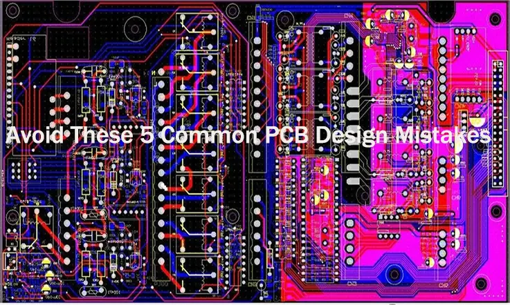
As technology advances, the demand for high-performance electronics continues to grow, and with it, the need for successful PCB design. A well-designed PCB ensures the reliable operation of electronic devices and prevents issues such as signal interference, power loss, and component failure. However, there are common mistakes that can occur during PCB design that can result in these issues. In this article, we will discuss the five most common PCB design mistakes and provide tips for avoiding them. By following these guidelines, you can ensure that your PCB designs are successful and reliable.
1.Inadequate Component Placement
Inadequate component placement is one of the most common PCB design mistakes. Poorly placed components can cause signal interference, power loss, and even component failure. To avoid this mistake, it’s important to consider the placement of each component carefully.
Here are some tips for proper component placement:
● Follow datasheet recommendations: Each component has its own datasheet, which provides guidelines for placement and orientation. Make sure to follow these recommendations to ensure optimal performance.
● Group components logically: Group related components together to minimize the length of traces and reduce the potential for interference.
● Consider thermal management: Components that generate heat, such as power transistors, must be placed in areas with adequate airflow or heat sinking.
By taking the time to carefully consider component placement, you can avoid this common PCB design mistake and ensure optimal performance.
2.Improper Trace Routing
Improper trace routing is another common PCB design mistake that can cause signal interference and power loss. Trace routing refers to the layout of electrical connections between components on a PCB. Poor routing can lead to problems such as signal reflections, crosstalk, and electromagnetic interference.
Here are some tips for proper trace routing:
● Use the shortest route possible: Minimizing the length of traces reduces the potential for signal loss and interference.
● Avoid sharp angles and corners: Smooth, flowing curves are better for signal transmission and reduce the risk of EMI.
● Follow design rules: PCB design software typically includes design rules to ensure proper trace spacing and clearance. Follow these rules to avoid issues such as short circuits.
By following these tips, you can ensure proper trace routing and avoid common PCB design mistakes.
3.Insufficient Clearances
Insufficient clearances between components and traces is another common PCB design mistake that can cause issues such as short circuits and signal interference. Clearances refer to the space between components, traces, and other elements on a PCB.
Here are some tips for proper clearance design:
● Consider minimum clearance recommendations: PCB design software and component datasheets typically provide recommendations for minimum clearances. Make sure to follow these guidelines to avoid issues.
● Allow for tolerances: Components and traces can shift slightly during manufacturing, so it’s important to allow for tolerances in your design.
● Consider high-voltage components: High-voltage components require larger clearances to prevent arcing and other issues.
By paying attention to clearance design, you can avoid common PCB design mistakes and ensure the reliable operation of your electronic devices.
4.Inadequate Power and Ground Planes
Inadequate power and ground planes are a common PCB design mistake that can cause power loss, signal interference, and even component failure. Power and ground planes are large areas of copper that provide a low-impedance path for power and ground signals.
Here are some tips for proper power and ground plane design:
● Use multiple planes: Multiple power and ground planes can reduce the potential for interference and provide a more stable power supply.
● Place planes close to signal layers: Placing power and ground planes close to signal layers reduces the length of vias and minimizes the potential for interference.
● Use a solid plane instead of a split plane: A solid plane provides better shielding and reduces the potential for EMI and other issues.
By following these tips, you can ensure proper power and ground plane design and avoid common PCB design mistakes.
5.Lack of DFM Considerations
Lack of DFM (Design for Manufacturability) considerations is a common PCB design mistake that can result in issues during the manufacturing process. DFM refers to designing a PCB with the manufacturing process in mind, to ensure that the final product is easily and efficiently produced.
Here are some tips for proper DFM considerations:
Use standard components: Using standard components reduces the risk of supply chain issues and ensures that the components are readily available for manufacturing.
Consider the manufacturing process: PCB design should take into account the limitations of the manufacturing process, such as the minimum size of drill holes and the maximum number of layers.
Test the design: Before sending the design to manufacturing, perform a design review and test the prototype to ensure that it can be manufactured efficiently.
By keeping DFM considerations in mind during the design process, you can reduce the risk of manufacturing issues and ensure that your PCB is produced efficiently and cost-effectively.
Conclusion
Designing a printed circuit board (PCB) requires a high level of technical expertise and precision. Even small mistakes made during the design process can result in significant losses. Therefore, it is critical to double-check the design to prevent low-quality products from being produced and reaching the market. In today’s market, consumers are increasingly demanding high-quality products, and PCBs are no exception. If you plan to manufacture a PCB, it is essential to consult an experienced industry expert first.
At JarnisTech, we are a reputable PCB manufacturer that offers a wide range of PCB solutions. Our clients have relied on us for decades to provide the best PCB solutions, designed by industry-tested professionals. By choosing our PCBs, you can ensure that your product will meet the highest quality standards.
There are several common mistakes to avoid during the PCB design stage, including inadequate component placement, improper trace routing, insufficient clearances, inadequate power and ground planes, and lack of DFM considerations. By paying close attention to these factors and working with experienced professionals, you can avoid these mistakes and produce a high-quality PCB that meets the needs of your customers.
Related Posts:
1. Everything You Should to Know on Altium PCB Design Software
2. Which One Are the Best Auto-route PCB Software?
3. PCB Traces: The Critical Role of Traces in PCB Design and Manufacturing
4. ExpressPCB Design Tool: A Comprehensive Guide to Using ExpressPCB
6. You Need to know the PCB Design Software: Eagle PCB
7. Kicad PCB: How to Understand It?
8. What Is the Difference Between Altium and Eagle?
9. How to Make a Arduino PCB – You Must to know Everything About It
10. EDA Design Software: Definition, Kinds and Important