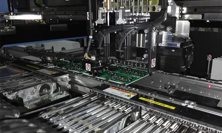
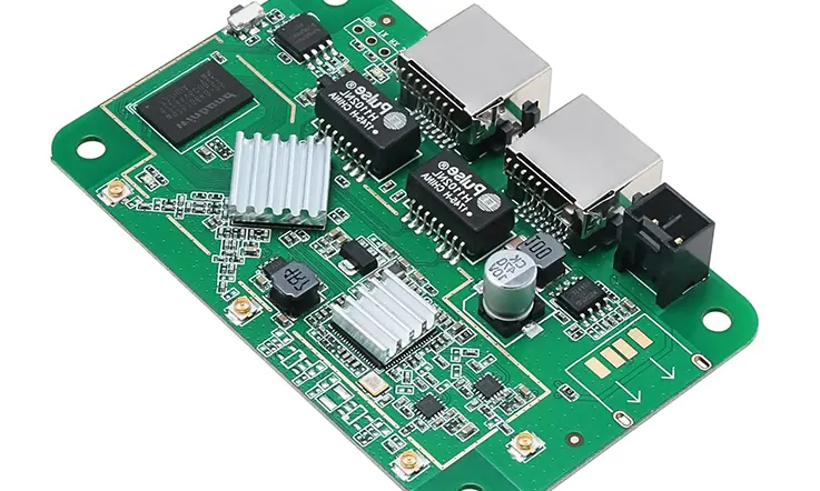
The assembly of electronic circuits via Surface Mount Technology (SMT) demands a profound understanding of materials science and process control. This text provides a systematic framework for professionals seeking to achieve high-yield, high-reliability solder connections. It moves from foundational principles to advanced process optimization, establishing a comprehensive guide to modern SMD soldering.
The Unchanging Foundation: Physics and Chemistry of the Solder Joint
A dependable solder joint originates from the application of fundamental physical and chemical laws. A command of these principles is a prerequisite for effective process control and troubleshooting, moving beyond procedural execution to achieve predictable, high-caliber results.
Wetting and Surface Tension
The formation of a solder joint relies on the principle of wetting: the ability of molten solder to spread across a solid surface, such as a PCB pad or component lead. This behavior stems from the interplay between the solder’s internal cohesive forces and the adhesive forces between the solder and the metallic surface. For a sound connection, adhesive forces must prevail, enabling the solder to flow and form a broad, smooth contact area.
●Contact Angle: This measurement gauges wetting effectiveness. A low contact angle signifies thorough wetting and a strong bond, whereas a high contact angle points to poor wetting and a probable joint defect.
●Surface Tension: An inherent property of liquids, surface tension causes molten solder to pull inward into a spherical shape. The soldering process, particularly the chemical action of flux, is engineered to reduce this tension, promoting the required spread and flow.
Formation of the Intermetallic Compound (IMC) Layer
A solder joint is a metallurgical connection created by an Intermetallic Compound (IMC) layer. This distinct alloy forms at the interface when molten solder reacts chemically with the copper (Cu) of the PCB pad and the component termination. This layer, typically just a few microns thick, provides the joint’s structural integrity and electrical continuity.
●Proper IMC Formation: A thin, uniform IMC layer (such as Cu₆Sn₅ and Cu₃Sn) is the objective for a durable, long-lasting connection.
●Risks of Excessive Growth: Extended soldering time or elevated temperatures can cause this layer to thicken. An overly thick IMC layer becomes brittle, making the joint susceptible to fracture under mechanical or thermal stress. Managing IMC growth is a primary goal of thermal profile optimization.
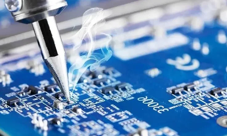
The Function of Flux in Oxide Removal
Metallic surfaces, particularly copper, naturally develop a thin oxide layer when exposed to air. This non-wettable film obstructs the molten solder, preventing a proper metallurgical bond. Flux is formulated to chemically remove these oxides immediately before and during soldering.
●Surface Cleaning: Flux contains activators, such as mild organic acids, that become reactive at soldering temperatures. As the assembly heats, the flux melts and its activators cleanse the metal oxides from the surfaces.
●Oxidation Prevention: After cleaning, the liquid flux covers the pristine metal. This temporary shield prevents re-oxidation in the hot, oxygen-filled environment of the reflow oven, leaving a clean surface available for the solder to bond with.
Precise management of these chemical and physical interactions is what separates a standard assembly from a high-reliability electronic product.
Process Control in the SMT Workflow
The Surface-Mount Technology (SMT) production line is a sequence of interdependent stages. A deviation in an early stage propagates through the workflow, affecting the final assembly’s quality. Effective process control, therefore, extends beyond task execution to include the monitoring and verification of each stage’s output with quantitative data.
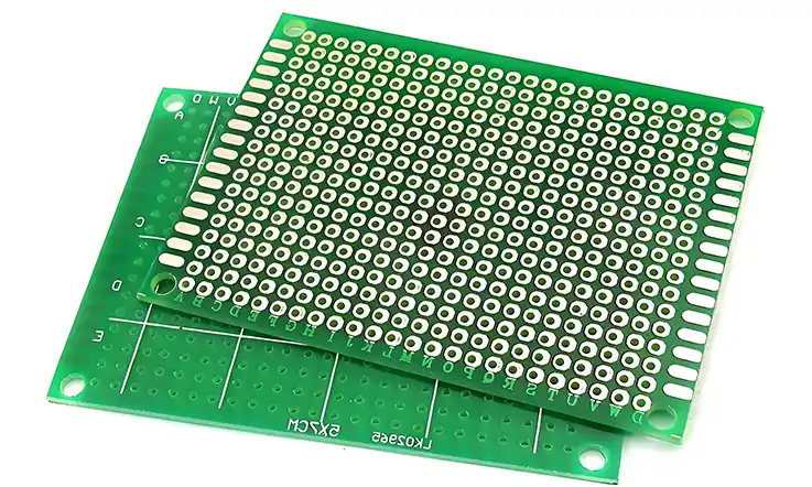
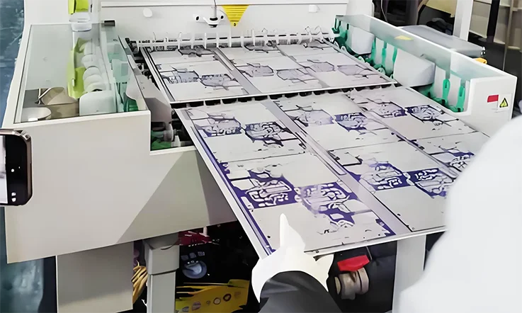
Stencil Printing: Accurate Paste Deposition
The stencil printing stage establishes the groundwork for the final solder joints. The objective here is the deposition of a precise and repeatable volume of solder paste onto every land pattern. The accuracy of this deposit directly influences defect rates for conditions such as bridging, opens, and insufficient solder.
●Stencil Fabrication: The stencil’s aperture design (dimensions and shape) and foil thickness collectively define the theoretical print volume. For fine-pitch components, stencils are fabricated using laser cutting and electropolishing to enhance paste transfer efficiency.
●Squeegee Mechanics: The squeegee’s pressure, speed, and angle of attack are calibrated to fill apertures completely without causing paste to scoop or smear, ensuring a clean print.
●3D SPI Verification: A 3D Solder Paste Inspection (SPI) system is integrated immediately after printing. This apparatus measures the volume, area, and height of every paste deposit, supplying immediate process feedback and preventing boards with printing defects from proceeding.
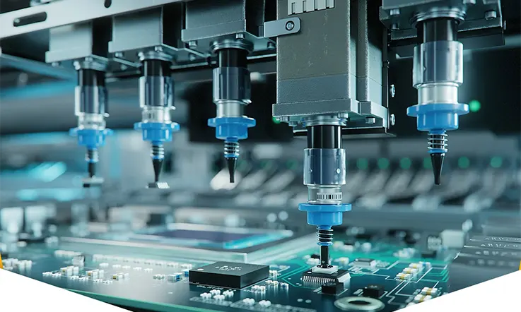
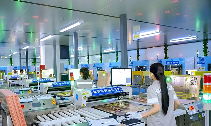
Component Placement: Positional and Force Precision
Following paste deposition, the assembly moves to automated component placement. Machines pick individual components, use vision systems to check identity and orientation, and then place them onto the corresponding pads.
●Placement Accuracy: The system must achieve high repeatable accuracy, often within ±25 µm, to correctly position fine-pitch packages like BGAs and 0201 components.
●Placement Force: The machine’s Z-axis applies a calibrated force to set the component securely into the paste without squeezing paste out from under the component body, which would cause bridging.
●Vision System: The integrated vision system serves a dual purpose: it aligns the component for placement and can identify parts with bent leads or other physical defects before they are mounted.
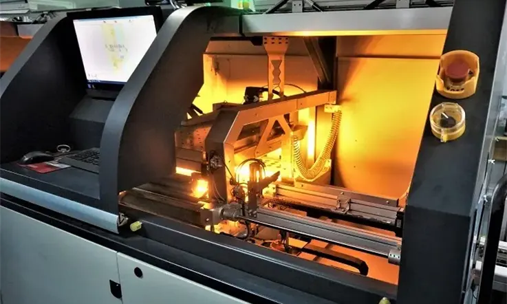
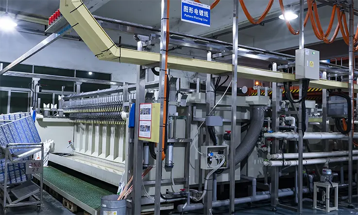
Reflow Oven Thermal Profiling
Once components are placed, the assembly enters the reflow oven where the solder joints are formed. This is not a passive heating step; it is a tightly controlled thermal process. A specific temperature-versus-time profile is developed for each assembly. This profile guides the PCB through several zones—preheat, soak, reflow, and cooling—to melt the solder paste and create a sound metallurgical bond without subjecting the components or the board to excessive thermal stress.
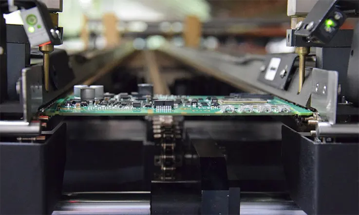
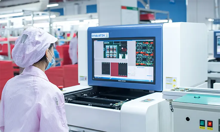
Post-Reflow Inspection: Automated Verification
After the assembly exits the reflow oven, a verification step confirms the process quality. This procedure is designed not merely to find defects, but to gather data that helps keep the manufacturing process centered and stable.
●Automated Optical Inspection (AOI): This high-speed, non-contact method employs cameras to examine the PCB surface. It is highly effective at detecting visible anomalies like missing components, incorrect polarity, solder bridging, and insufficient solder.
●Automated X-ray Inspection (AXI): This method is applied to components with hidden solder joints, such as Ball Grid Arrays (BGAs). X-rays penetrate the component, generating an image of the underlying connections to check for shorts, opens, voids, and other concealed defects.
Thermal Profile Optimization in Reflow Soldering
The reflow oven facilitates the transformation of solder paste into a solid metallurgical connection. This transformation is governed by the thermal profile—the precise temperature sequence an assembly experiences over time. Engineering a correct profile is a demanding aspect of SMT assembly, requiring a balance between the thermal needs of diverse components and materials on a single board.
The Four Zones of a Reflow Profile
A standard reflow profile is segmented into four distinct zones, each with a specific thermodynamic function. Successful passage through each zone prepares the assembly for the next.
1. Preheat Zone: The assembly undergoes a controlled, linear temperature rise (typically 1–3°C per second). This gradual ramp prevents thermal shock to components and allows volatile solvents in the solder paste to outgas safely.
2. Soak Zone: The temperature is held at a constant plateau (e.g., 150–200°C) for 60–120 seconds. This stage allows the temperature to equalize across the entire board, minimizing temperature differentials (ΔT) and ensuring the flux is fully activated before reflow.
3. Reflow Zone: The temperature is rapidly increased past the solder’s liquidus point. The duration that the assembly spends above this point, or Time Above Liquidus (TAL), is typically 30–90 seconds. This allows the solder to melt, wet the component and pad surfaces, and form the intermetallic (IMC) layer.
4. Cooling Zone: The final stage is a controlled cooling ramp (e.g., -2 to -4°C per second). A carefully managed cooling rate promotes the formation of a fine-grain microstructure in the solder, which yields superior mechanical strength and prevents the growth of thick, brittle IMC layers.
Zone
Function
Typical Temperature / Rate
Typical Duration
Preheat Zone
Controlled temperature ramp to avoid thermal shock, allow solvent outgassing
1–3 °C/sec ramp to ~150°C
60–120 sec
Soak Zone
Equalize board temperature, activate flux
150–200°C plateau
60–120 sec
Reflow Zone
Melt solder, wet surfaces, form IMC
Peak 235–250°C, TAL 30–90 sec
30–90 sec above liquidus
Cooling Zone
Control cooling to refine solder microstructure, prevent brittle IMC growth
-2 to -4 °C/sec cooling rate
Until < 100°C
Profiling Strategies for Complex Assemblies
A generic profile is inadequate for complex circuit boards. Assemblies with a high mix of component sizes, large copper planes, or high overall thermal mass present a challenge to achieving temperature uniformity.
●Profile Adjustment: For such boards, a profile with a pronounced soak plateau is generally selected. This provides the necessary time for large components to reach the same temperature as smaller parts. Thermocouples are attached to the board at various locations to measure the actual temperature profile as it passes through the oven. The oven’s zone setpoints are then iteratively adjusted until the measured profile falls within the desired process window.
●Process Window Index (PWI): To quantify the profile’s robustness, the Process Window Index (PWI) is calculated. This metric statistically measures how well the profile fits within the specifications of the solder paste and components. A PWI below 100% indicates a capable and centered process.
Parameter
Typical Range / Example
Purpose
Soak Plateau Temperature
150–200°C
Equalizes large & small component temperature
Soak Duration
60–120 sec
Allows flux activation & ΔT reduction
Number of Thermocouples
3–5+ (varied board positions)
Measure actual temperature at critical points
PWI Target
< 100%
Ensures process is within solder/component limits
The Utility of Vacuum Reflow Technology
Void formation within solder joints is a persistent defect that can compromise a product’s thermal and mechanical durability. Vacuum reflow soldering is an advanced process engineered to address this issue.
●Process: In a vacuum reflow system, after the solder becomes molten, the process chamber is subjected to a partial vacuum.
●Mechanism: This reduction in ambient pressure allows any trapped gas bubbles—originating from flux volatiles—to expand and escape from the liquid solder.
●Result: This technology substantially reduces void percentages in solder joints. This level of performance is frequently a requirement for high-reliability assemblies in the automotive, aerospace, and medical fields.
Assembly Methodologies for Advanced Component Packages
The progression toward smaller and more powerful electronics relies on the adoption of advanced component packages. These packages, while enabling superior density and performance, have specific design characteristics that demand specialized knowledge and refined assembly techniques.
Soldering Considerations for BGA and CSP
Ball Grid Array (BGA) and Chip Scale Packages (CSP) feature connections on the component’s underside, making both assembly and inspection complex. A successful outcome depends on precise solder paste deposition and diligent warpage control.
●Paste Volume Control: The stencil printing process is engineered to deposit a precise volume of solder paste onto each pad, with the accuracy of every deposit verified by 3D Solder Paste Inspection (SPI).
●Warpage Mitigation: A carefully developed thermal profile, often featuring a slow ramp rate and an extended soak phase, minimizes the thermal gradients across the board and package that can induce warpage.
●Post-Reflow Inspection: After assembly, 3D Automated X-ray Inspection (AXI) is the definitive method for examining internal features, including voids, shorts, and the subtle Head-in-Pillow (HiP) defect.
●Underfill Application: For applications requiring enhanced mechanical durability, an underfill epoxy can be dispensed beneath the component after reflow. This process reinforces the solder joints, improving their resilience to shock and vibration.
Managing the Thermal Pad on QFN and DFN Packages
Quad Flat No-lead (QFN) and Dual Flat No-lead (DFN) packages are selected for their excellent thermal dissipation, facilitated by a large, exposed pad on their underside. This feature, however, introduces a common soldering challenge.
●The Defect Mechanism: Applying a single, large solder paste deposit to the thermal pad can trap significant voiding. It can also cause the lightweight component to float on the surface of the molten solder, preventing its perimeter I/O pads from making proper contact with the PCB.
●The Stencil Solution: A “window-pane” or “checkerboard” aperture design is implemented in the stencil. This strategy divides the single large deposit into multiple smaller ones. This approach provides outgassing channels for flux volatiles to escape and reduces the net surface tension, allowing the component to seat correctly.
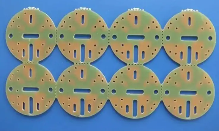
Assembly of 0201 and 01005 Passive Components
The assembly of ultra-small passive components, such as those in the 0201 and 01005 footprints, requires process control at its most stringent. At this scale, minute process variations can result in defects.
●Printing Materials: A thin stencil foil (e.g., 75-100 microns) combined with a fine-particle solder powder (Type 5 or smaller) is used to accurately print the minuscule solder deposits.
●Placement Mechanics: The placement equipment must offer exceptional positional accuracy and apply a minimal placement force to avoid disturbing the paste or damaging these fragile components.
●Defect Prevention: The “tombstoning” defect, where a component stands on one end, is a frequent issue. It is effectively prevented through symmetrical PCB pad design and a highly uniform thermal process during reflow.
Techniques for Package-on-Package (PoP) Assembly
Package-on-Package (PoP) technology, which involves stacking components like a processor on top of a memory module, represents a further step in three-dimensional integration. This assembly process requires managing the complexities of two separate reflow interfaces and controlling warpage across both the top and bottom packages to ensure a reliable final connection.
Systematic Defect Analysis and Root Cause Elimination
A mature manufacturing operation is defined by its methodical approach to quality control. This involves not only identifying production anomalies but also employing formal Root Cause Analysis (RCA) to eliminate their source. By using Statistical Process Control (SPC) to monitor production data, process deviations can be addressed before they result in defects, moving from reactive inspection to proactive quality assurance.
Defects Related to Solder Paste Deposition
A large portion of all SMT defects can be traced to the stencil printing stage. An understanding of these common issues allows for targeted corrective action.
●Insufficient Solder: This defect, appearing as open circuits or weak joints, is often caused by clogged stencil apertures or poor paste release from the foil.
●Solder Bridging: The creation of unintended short circuits between adjacent pads is typically the result of excessive solder paste, stemming from oversized apertures or paste smearing during the print cycle.
●Solder Balling: Small, unwanted spheres of solder on the board surface are frequently caused by excessive moisture in the solder paste or miscalibrated component placement pressure.
Defects Originating from the Reflow Process
The thermal profile represents a delicate balance of heat and time. Deviations from the target profile manifest as distinct types of manufacturing defects.
●Tombstoning: This effect, where a chip component lifts on one end, is caused by an imbalance in wetting forces. This imbalance usually results from a significant temperature differential (ΔT) between the component’s two terminal pads during reflow.
●Cold Solder Joints: Characterized by a dull and grainy appearance, these unreliable joints are the product of insufficient heat, either due to a low peak temperature or an inadequate Time Above Liquidus (TAL).
●Overheated Assemblies: Charred sections of the PCB or visibly damaged components are unambiguous signs of excessive heat exposure, necessitating a downward adjustment of the oven’s thermal profile.
Hidden Defects and Their Detection
Some of the most challenging defects are those that cannot be seen with optical inspection. These require Automated X-ray Inspection (AXI) for detection and are often linked to complex interactions between the circuit design, materials, and process variables.
●Voiding: Diagnosed with AXI, voids are trapped gas bubbles that originate from flux volatiles. This is addressed by optimizing the thermal profile’s outgassing phases and refining the stencil aperture design for large pads.
●Head-in-Pillow (HiP): This is a non-wetted interface under a BGA, often caused by component warpage during reflow or premature exhaustion of the flux’s activity. Its reliable detection requires the capabilities of 3D AXI.
Proactive Prevention Through Design for Manufacturability (DFM)
The most effective form of defect prevention occurs before production begins. A comprehensive Design for Manufacturability (DFM) analysis examines the PCB layout data to identify and rectify potential issues. By correcting problematic features—such as asymmetrical pad designs that can lead to tombstoning or poor thermal reliefs that affect heat distribution—many of the defects discussed above can be eliminated at the design stage. This approach embodies a foundational principle of high-reliability manufacturing: quality is engineered, not just inspected.
Solder Joint Reliability and Long-Term Performance Verification
Initial post-assembly functionality is a baseline expectation; the more demanding objective for many electronic products is ensuring the solder joints survive years of service in their intended environment. This requires an understanding of long-term failure mechanisms and validation through rigorous reliability testing.
Thermomechanical Fatigue and Failure Mechanisms
Most electronic assemblies are subjected to temperature fluctuations during operation. Due to the differing Coefficients of Thermal Expansion (CTE) between the component, the solder, and the PCB substrate, these temperature cycles induce mechanical stress and strain in the solder joints.
Over many cycles, this repeated strain leads to the initiation and propagation of microcracks, a phenomenon known as low-cycle fatigue. Eventually, these cracks can grow to a point of electrical failure.
Parameter
Typical Range / Value
Effect on Fatigue Life
CTE (PCB FR-4)
~14–17 ppm/°C
Mismatch with components causes joint strain
CTE (Ceramic package)
~6–8 ppm/°C
Higher mismatch with FR-4 increases stress
Solder Alloy Example (SAC305)
CTE ~22–24 ppm/°C
Differential expansion drives cyclic fatigue
Typical Thermal Cycle Range
-40°C to +125°C
Widely used in automotive/aerospace reliability testing
Coffin-Manson Exponent (n)
1.5–2.0
Material constant in fatigue life prediction
●Influencing Factors: The fatigue resistance of a joint is affected by the solder alloy itself, the quality of the intermetallic (IMC) layer, the geometry of the solder fillet, and the magnitude of the temperature swings.
●Predictive Models: Engineering models like the Coffin-Manson equation are employed in reliability engineering to help predict the functional lifetime of a joint under specific thermal cycling conditions.
The Effect of Voiding on Long-Term Reliability
While small, well-dispersed micro-voids may be acceptable, large voids or a high percentage of voiding can degrade long-term performance.
Parameter
Typical Acceptable Level
Impact if Exceeded
IPC-A-610 Class 2 Voiding
≤ 25% area in BGA/X-ray view
Higher risk of mechanical fatigue and heat buildup
IPC-A-610 Class 3 Voiding
≤ 10% area
Critical for aerospace, medical, and automotive
Large Single Void Diameter
≤ 1/3 of pad diameter
Increases crack initiation likelihood
Thermal Conductivity Loss
Up to 40% if >30% void area
Higher component junction temperature
Void Reduction with Vacuum
50–90%
Improves both mechanical and thermal performance
●Mechanical Degradation: Voids reduce the load-bearing cross-sectional area of the joint. This diminishes its ability to withstand shock and vibration and can serve as initiation sites for fatigue cracks.
●Thermal Impedance: In joints designed for thermal conduction, voids act as insulators. They impede the transfer of heat away from a component, causing it to operate at a higher temperature and potentially shortening its operational life. The use of advanced techniques like vacuum reflow soldering is a direct countermeasure to mitigate such voiding.
Methods of Reliability Testing
To validate the long-term performance of an assembly, products undergo various forms of accelerated testing. These protocols are designed to induce potential field failures within a compressed timeframe inside a laboratory setting.
Test Method
Typical Conditions
Purpose
Thermal Cycling
-40°C to +125°C, 500–2000 cycles
Simulates thermomechanical fatigue from environmental changes
Mechanical Shock
1500–3000 g, 0.5 ms pulse
Evaluates structural robustness against sudden impacts
Vibration Test
5–500 Hz, multi-axis
Simulates shipping and operational vibration stress
HALT (Highly Accelerated Life Test)
Temperature extremes: -100°C to +200°C + random 6-axis vibration
Determines operational/destruct limits of a design
HAST (Highly Accelerated Stress Test)
130°C, 85% RH, 96–192 hours
Accelerates corrosion/moisture-induced failure
●Thermal Cycling: The assembly is cycled between temperature extremes (e.g., -40°C to +125°C) to assess its resistance to thermomechanical fatigue.
●Mechanical Shock and Vibration: The assembly is subjected to controlled drops or multi-axis vibrations to simulate mechanical stresses and verify the structural integrity of the solder joints.
●Highly Accelerated Life Test (HALT): This method uses combined, stepped stresses (e.g., extreme temperature cycling and random six-axis vibration) to rapidly uncover the operational and destruct limits of a design, exposing inherent weaknesses.
●Highly Accelerated Stress Test (HAST): The assembly is exposed to high temperature and high humidity to accelerate failure mechanisms related to moisture ingress and corrosion.
Achieving lasting product reliability is the outcome of a holistic manufacturing philosophy. It is a systematic process that integrates a deep understanding of material science, precise control over each stage of production, the application of advanced assembly techniques, and validation through rigorous, targeted life testing.
PCB Material and Surface Finish Considerations in Soldering
The outcome of the soldering process is not determined by solder and flux alone. The Printed Circuit Board is an active component in this thermal process, and its material properties and surface preparation are foundational to achieving a reliable result. An understanding of these interactions is a prerequisite for robust assembly design.
Substrate Materials: FR-4 vs. High-Frequency Laminates
While FR-4, a glass-reinforced epoxy laminate, is the industry standard, high-frequency applications demand substrates with specialized dielectric properties, which in turn affects thermal processing.
●Material Differences: Substrates like Rogers or Teflon provide lower signal loss but possess different thermal characteristics compared to FR-4. A profile developed for an FR-4 board may induce excessive stress or require different ramp rates when applied to these materials due to variations in thermal conductivity and expansion.
●Glass Transition Temperature (Tg): This property indicates the temperature at which the substrate begins to transition from a rigid state to a softer, rubbery state. A material with a higher Tg exhibits greater stability at the elevated temperatures of lead-free soldering, reducing the likelihood of board warpage or delamination during the reflow process.
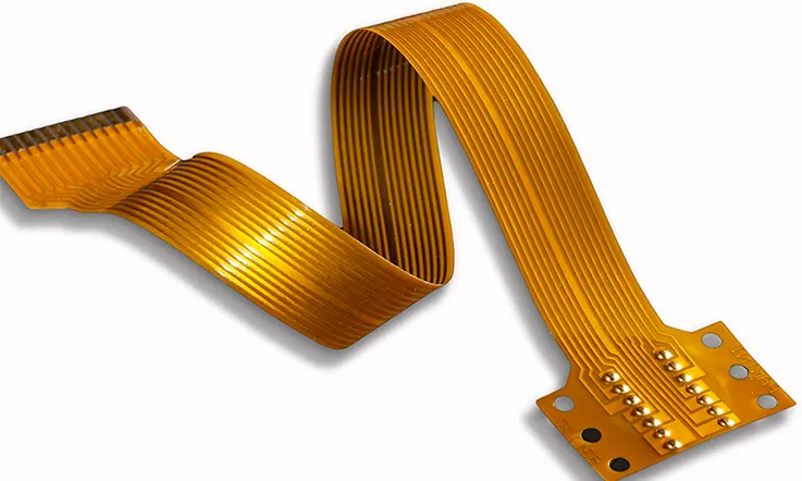
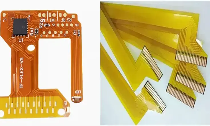
Assembly of Flexible Circuits (Polyimide)
Flexible circuits, typically fabricated from polyimide, introduce unique mechanical considerations to the soldering process.
●Handling and Fixturing: As flexible circuits are not self-supporting, they require rigid carriers or pallets to hold them flat and maintain dimensional stability throughout the SMT printing, placement, and reflow stages.
●Thermal Management: Polyimide has a much lower thermal mass than rigid FR-4 and consequently heats more rapidly. The reflow profile must be adjusted (e.g., with lower temperature setpoints or faster ramp rates) to prevent overheating and damaging the delicate substrate.
The Influence of PCB Surface Finish
The surface finish applied to the copper pads is a critical interface between the bare board and the solder joint. It dictates solderability, process window, and long-term reliability.
●HASL (Hot Air Solder Leveling): A cost-effective and robust finish providing excellent solderability. However, its uneven surface topology makes it less suitable for fine-pitch components.
●ENIG (Electroless Nickel Immersion Gold): Offers a very flat surface, ideal for fine-pitch packages and BGAs. It has a good shelf life but is a more complex and costly process.
●OSP (Organic Solderability Preservative): A flat, cost-effective finish applied in a simple process. It is sensitive to handling and can typically endure fewer reflow cycles compared to metallic finishes.
Moisture Sensitivity and Prevention
PCB substrate materials, especially FR-4, are hygroscopic, meaning they absorb moisture from the ambient environment.
●The “Popcorning” Defect: If a moisture-laden board is exposed to the rapid heating of reflow, the trapped moisture violently turns to steam, causing internal delamination of the PCB’s layers or blistering.
●Pre-Assembly Baking: To prevent this, boards are baked in calibrated ovens before assembly to drive out any absorbed moisture. IPC-1601 provides detailed guidelines for bake times and temperatures based on the board’s thickness, layer count, and storage history.
Understanding the interplay between substrate, surface finish, and the assembly process allows for potential issues to be mitigated at the design and fabrication stage, a distinct advantage of an integrated manufacturing approach.
Process Environment Control: ESD, Moisture, and Cleanliness
High-reliability electronics manufacturing extends beyond machinery and materials to encompass the entire production environment. The rigorous control of electrostatic discharge (ESD), moisture sensitivity, and particulate contamination is a foundational requirement for building products that are free from latent defects and dependable over their entire service life.
Electrostatic Discharge (ESD) Control
Many modern electronic components can be damaged or destroyed by electrostatic discharge. An ESD event can cause immediate, catastrophic failure or, more deceptively, inflict latent damage that leads to unexpected field failures months or years after shipment. A comprehensive ESD control program, compliant with standards like ANSI/ESD S20.20, is therefore implemented.
●Protective Measures: This program includes grounding for all personnel via wrist straps, the use of ESD-safe work surfaces and flooring, air ionization to neutralize charges, and the mandatory storage and transport of all sensitive items in static-shielding packaging.
●General Climate Control: The entire production floor is maintained within a specific temperature and relative humidity range. This stable climate is not only for operator comfort and process consistency but also serves as a primary method for mitigating the build-up of static electricity.
Moisture Sensitivity Level (MSL) Management
Plastic-encapsulated microcircuits are hygroscopic and absorb moisture from the air. If not properly controlled, this trapped moisture can rapidly expand during reflow, causing internal cracks in the component—a defect similar to the “popcorning” seen in bare PCBs.
●The J-STD-020 Standard: This industry standard classifies components into different Moisture Sensitivity Levels (MSLs), from 1 (least sensitive) to 6 (most sensitive), dictating their allowable exposure time to ambient conditions.
●Process and Traceability: A robust MSL program involves receiving components in sealed, moisture-barrier bags with desiccant. Once a bag is opened, a traceability system tracks the component’s “floor life.” If exposure limits are exceeded, components are baked in calibrated ovens according to J-STD-033 guidelines before use.
Cleanliness and Foreign Object Debris (FOD) Prevention
Particulate contamination and Foreign Object Debris (FOD) can introduce random, difficult-to-diagnose defects such as short circuits or mechanical interference.
●Controlled Environments: High-reliability assembly is performed within controlled cleanroom environments, classified according to ISO 14644 standards, to limit airborne particulate levels.
●FOD Program: A strict FOD prevention program is enforced, which includes the use of cleanroom garments, control over all materials entering the area, specialized cleaning procedures, and regular audits to eliminate contamination risks from sources like dust, fibers, or metal slivers.
These environmental disciplines are non-negotiable elements of a manufacturing process designed to deliver products with exceptional long-term reliability.
IPC Standards: A Framework for Assembly Quality and Reliability
In the global electronics industry, a common lexicon for quality is a necessity. The standards published by IPC (Association Connecting Electronics Industries) provide this objective benchmark. Adherence to these standards signifies a disciplined, mature, and quality-focused manufacturing process, offering a universally understood measure of workmanship.
Navigating IPC-A-610 Acceptability Classes
The IPC-A-610, “Acceptability of Electronic Assemblies,” is the most widely used visual inspection standard in the industry. It provides clear, photographic examples of acceptable conditions and defect conditions for solder joints and assemblies. The standard defines three classes of product.
●Class 1 – General Electronic Products: Applies to consumer goods where the primary requirement is the function of the completed assembly.
●Class 2 – Dedicated Service Electronic Products: For equipment where continued performance and an extended service life are expected, though uninterrupted service is not a defining feature.
●Class 3 – High Performance/Harsh Environment Electronic Products: Reserved for fields such as aerospace, military, and medical systems, where assemblies must function with an extremely high level of dependability. This class imposes the most stringent acceptance criteria.
J-STD-001: The Process Requirement Standard
While IPC-A-610 defines “what” a product should look like, the J-STD-001, “Requirements for Soldered Electrical and Electronic Assemblies,” defines “how” it should be built. A manufacturing process certified to J-STD-001 demonstrates a commitment to a controlled, repeatable, and high-reliability production methodology.
●Scope: This standard specifies the materials, methods, and verification criteria necessary for producing high-quality soldered interconnections. Its scope is comprehensive, covering everything from flux and solder requirements to thermal profiling and operator proficiency.
The Value of Certified Personnel and Processes
Adherence to IPC standards is more than just owning a document; it is about embedding the knowledge within the workforce and processes.
●Operator and Inspector Certification: A commitment to quality is demonstrated by having personnel trained and certified as Certified IPC Specialists (CIS). This ensures that the individuals building and inspecting the product have a deep, verified understanding of the standards.
●Controlled Rework and Repair: In addition to initial assembly, processes for any necessary rework or repair also follow stringent guidelines, as defined by the IPC-7711/7721 standard. This ensures that even corrected assemblies meet the highest quality and reliability requirements.
Ultimately, the IPC standards provide the overarching framework that governs all the disciplines discussed in this series. From the material science of substrates and the physics of the solder joint, through the precise execution of process controls, to the final verification with reliability testing—all these activities are guided and validated by this common, objective language of quality.
Frequently Asked Questions (FAQ)
This section provides concise answers to common queries regarding the SMT soldering process and related technologies.
Q: What is the difference between a soak and a ramp-to-spike (RTS) thermal profile?
A: A soak profile uses a temperature plateau to equalize temperature on complex boards, minimizing thermal stress. An RTS profile is a faster, continuous ramp best for simple boards with uniform thermal mass.
Q: How is the voiding percentage in a solder joint measured and what is an acceptable limit?
A: Voiding is measured with an X-ray (AXI) system. Acceptable limits depend on the product class per standards like IPC-7095, but are often below 15-25% for high-reliability BGA solder balls.
Q: What is the difference between a “via-in-pad” and a “dog-bone” via connection?
A: A dog-bone connects a pad to an adjacent via with a short trace. A via-in-pad places the via directly in the pad for denser designs but must be filled and plated flat during fabrication to prevent soldering defects.
Q: Can different solder alloys be mixed in a single assembly process?
A: This is not recommended. Mixing alloys creates unpredictable, brittle intermetallics that compromise long-term reliability and make process control difficult.
Q: Does a “no-clean” flux truly require no cleaning after soldering?
A: Mostly, yes; the residues are designed to be benign. However, for certain high-reliability applications, cleaning may still be performed to ensure electrical performance or proper adhesion of conformal coatings.
Q: Why is a Design for Manufacturability (DFM) analysis recommended before fabrication?
A: A DFM analysis checks a PCB layout for features that could cause manufacturing or assembly defects. It proactively improves yield, reduces costs, and prevents problems by correcting the design before production begins.
A Partner in High-Reliability Manufacturing
Executing the complex processes of modern electronics assembly demands more than theoretical knowledge. It requires a synthesis of experience, advanced technology, and a systematic commitment to precision. This is a look into that methodology.
A Foundation of Quality
A robust Quality Management System (QMS) is the foundation of the entire operation, ensuring traceability, process stability, and continuous improvement.
●Adherence to IPC Standards: Operations are conducted in strict accordance with industry standards, with demonstrated capabilities to meet IPC-A-610 Class 2 and Class 3 requirements. This ensures your products are built to the level of reliability your application demands.
●Advanced Inspection and Data: Investment in state-of-the-art inspection technology, including 3D Automated Optical Inspection (AOI) and 3D Automated X-ray Inspection (AXI), allows not only for defect detection but also for the collection of process data. This data is used to keep all processes perfectly calibrated, preventing anomalies from occurring.
●Rigorous Process Control: From incoming material verification to final functional testing, every stage is governed by documented process controls, ensuring the final product precisely matches the design intent.
Value Through Efficiency and Transparency
Project success depends on effective budget management. Exceptional value is delivered through operational efficiency and financial transparency.
●Optimized Supply Chain: Established relationships with a global network of component suppliers allow for the sourcing of high-quality parts at competitive prices, minimizing procurement delays.
●Efficient Manufacturing: Investment in modern equipment and process optimization reduces manufacturing time and material waste, with these efficiency savings reflected in the final cost.
●Detailed and Clear Quotations: Quotations are comprehensive and transparent. A clear breakdown of costs is provided with no hidden fees, allowing for accurate and dependable project budgeting.
Predictability and On-Time Delivery
Meeting deadlines is a baseline requirement in the electronics market. The entire workflow is engineered for predictability and on-time delivery.
●Structured Project Management: Each project is assigned a dedicated manager who provides a clear schedule and regular status updates, ensuring clients are always informed.
●Flexible Timelines: A range of service options is available to match project needs, from rapid prototyping with expedited turnarounds to scheduled high-volume production.
●A Proven Record: A strong history of on-time delivery is a core performance metric, born from an understanding of the high cost of project delays.
Expert Engineering and Project Support
A successful partnership is built on clear communication and expert technical support.
●Engineering Consultation: Access to experienced engineers is available for complimentary Design for Manufacturability (DFM) and Design for Assembly (DFA) feedback. Identifying potential issues before production helps save time and resources on costly revisions.
●Single Point of Contact: Clients work with a dedicated representative who understands the project’s technical and commercial requirements, ensuring communication is always clear and effective.
●Responsive Communication: A commitment to responsiveness ensures technical queries and schedule updates receive prompt and helpful answers.
Advanced Manufacturing Capabilities
The facility and processes are equipped to handle the challenges of modern electronics design, from the straightforward to the highly complex.
●Advanced Component Handling: Proven processes are in place for assembling ultra-fine pitch components down to 01005, as well as complex packages including BGAs, CSPs, and QFNs.
●Technology Portfolio: Capabilities include advanced soldering techniques such as vacuum reflow for void reduction and selective soldering for mixed-technology boards.
●Material & Finish Flexibility: Support is provided for a vast range of PCB substrates, including FR-4, Rogers, Teflon, and Flex/Rigid-Flex materials, along with all major surface finishes like ENIG, ENEPIG, ImAg, and OSP.
Begin a Partnership Built on Expertise
The technical proficiency detailed throughout this guide is the basis of a reliable manufacturing partnership. To see how this expertise can be applied to your specific project, submit your design for a complimentary DFM analysis or request a detailed quotation today.
Modern electronic systems require printed circuit boards (PCBs) engineered to perform under conditions that surpass conventional limitations. As device functionality, speed, and power density increase, the demand for circuit boards tailored to specific, high-performance applications becomes a necessity. This guide provides a technical exploration of specialized PCBs, detailing their architectures, the advanced materials used, and the complex fabrication and assembly processes involved in their creation, all while adhering to stringent industry quality standards.
Specialized PCBs: From Precision Fabrication to Full Assembly
A specialized printed circuit board is engineered to perform in applications where standard boards are insufficient. Its construction involves non-standard materials, intricate layouts, and specific electrical properties to achieve superior performance and durability in demanding environments. This fabrication approach moves beyond generic templates to satisfy precise operational requirements.
Following the custom fabrication of the board, the assembly process populates it with electronic components. This stage continues the dedication to precision, transforming a bare board into a fully operational unit ready for its intended function. The assembly service encompasses:
Component Sourcing:
Procurement of all specified electronic components, which includes managing complex supply chains for specialized or long-lead-time parts.
SMT & Thru-Hole Assembly:
Application of automated techniques for exact component placement on any board topology, including dense, double-sided, and mixed-technology assemblies.
Quality Verification:
Post-assembly inspection and functional testing to confirm that every connection and component placement adheres to stringent project specifications.
Turnkey Assembly Service:
An end-to-end process that delivers a fully assembled and tested product, prepared for final system integration.
An Overview of Specialized PCB Architectures
Specialized printed circuit boards are engineered for challenges that standard boards cannot address. Each design provides a distinct solution for specific mechanical, thermal, or spatial constraints, forming the foundation for high-performance electronic devices.
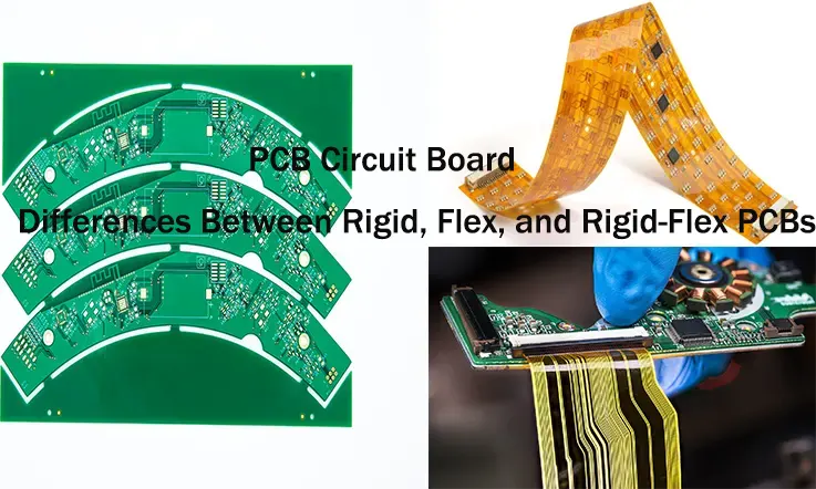
Flexible PCBs (Flex Circuits)
Constructed on pliable polymer substrates, flexible circuits can bend and fold to integrate into three-dimensional product enclosures. They offer a direct replacement for rigid boards connected with wires and connectors, especially in applications where space and weight are limited.
●Three-Dimensional Integration: Flex circuits conform to the internal contours of a product, saving significant space and weight compared to rigid board and cable harness combinations.
●Dynamic Applications: Their resilience to repeated movement makes them suitable for hinged electronics, robotics, and other applications requiring interconnection between moving parts.
●Verified Reliability: Performance is qualified against demanding standards like IPC-6013, ensuring durability for use in wearables, medical implants, and aerospace systems.
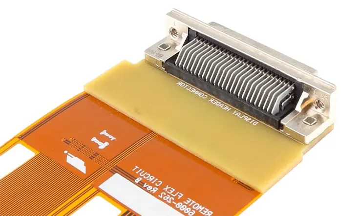
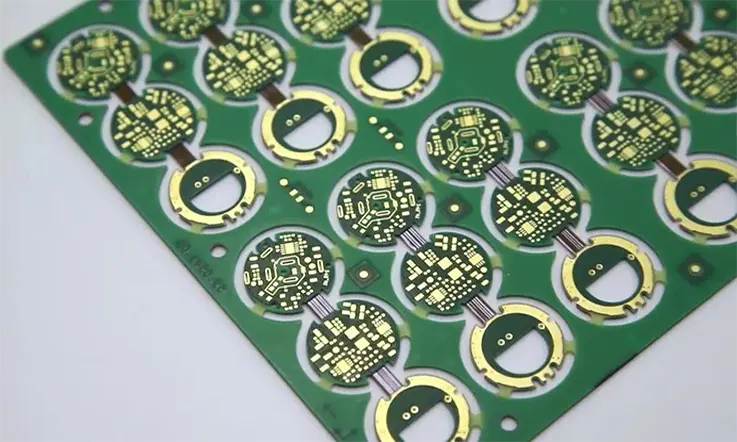
These boards are a hybrid, combining rigid PCB sections and flexible circuits into a single, unified component. The design provides the mounting stability of a rigid board for dense component populations while offering the routing freedom of a flex circuit to interconnect these sections, which removes potential points of failure from separate cables and connectors.
Application Example: 8-Layer Rigid-Flex PCB for an Aerial Drone Gimbal
●Challenge: A three-axis camera gimbal experienced signal degradation and mechanical wear from traditional cable connections subjected to constant rotation and stress.
●Solution: An 8-layer rigid-flex board was engineered. Rigid sections provided stable platforms for the image sensor and processors, while an integrated flex tail replaced the wiring harness, moving freely with the gimbal.
●Result: The unified design resolved all connection reliability issues. It also reduced the gimbal’s weight by 25%, contributing to longer flight times, and streamlined final assembly by removing manual connection points.
Parameter
Typical Value/Range
Industry Benchmark
Total Layer Count
4–20 layers
≥ 8 for complex apps
Flex Section Thickness
0.1–0.2 mm
IPC-2223 standard
Bend Cycles (Dynamic)
> 500,000
IPC-6013 Class 3
Weight Reduction
20–30%
Verified in teardown
Integration Efficiency
1 unified PCB vs. ≥ 3 separate parts
Reduced interconnect failures
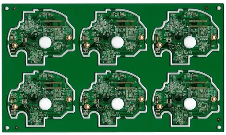
High-Density Interconnect (HDI) PCBs
High-Density Interconnect (HDI) manufacturing enables a higher concentration of components and routing per unit area. This is achieved with features like laser-drilled microvias, finer traces and spaces, and advanced lamination processes, facilitating substantial device miniaturization without sacrificing functionality.
Application Example: HDI Mainboard for a Portable Medical Monitor
●Challenge: A medical device required an extremely small, wearable glucose monitor with powerful processing and extended battery life.
●Solution: A 10-layer HDI board with a (1+8+1) sequential build-up (SBU) structure was used. Stacked microvias and via-in-pad technology allowed a 0.4mm pitch BGA processor and all support circuits to be placed on a board the size of a postage stamp.
●Result: The product’s footprint was reduced by 60%. Shorter signal paths lowered power consumption, extending battery life by 40%. The HDI structure also provided a stable platform for the assembly of the fine-pitch BGA.
An MCPCB is built on a metal base, typically aluminum or copper, for superior thermal dissipation. An electrically isolating, thermally conductive dielectric separates the circuit from the metal core, drawing heat away from power-intensive components more effectively than standard FR-4 substrates.
Application Example: Aluminum Core PCB for an Industrial LED High-Bay Light
●Challenge: A 200W LED high-bay light suffered from rapid lumen decay and a short operational life due to heat accumulation on its standard FR-4 board.
●Solution: The light engine was redesigned using a high-performance aluminum core PCB. The aluminum base efficiently transferred heat from the LED array to the fixture’s external heatsink.
●Result: The LED chips’ junction temperature dropped by a measured 35°C. This change stabilized the light output and more than doubled the luminaire’s effective lifespan.
Parameter
Typical Value/Range
Industry Benchmark
Core Material
Aluminum or Copper
≥ 1.5 mm thick
Thermal Conductivity
1.5–3.0 W/m·K
≥ 2.0 W/m·K
Max Operating Power
50–300 W
LED lighting spec
Junction Temperature Drop
25–40°C improvement
Verified in lab
Lifespan Improvement
2×–3×
Field-tested
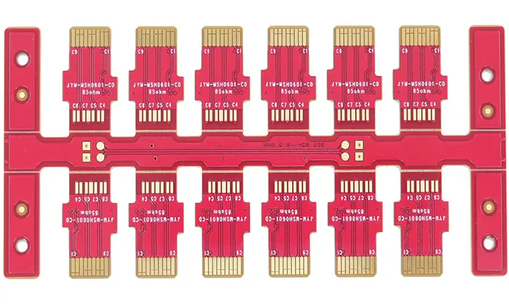
Thick Copper PCBs
This category includes PCBs with copper layers exceeding the standard 1-2 oz (35-70µm) thickness. Designed for high-current applications, these boards use heavy copper traces to manage large electrical loads and aid in thermal distribution across the board.
●High-Current Capacity: With copper weights from 3 oz to over 10 oz, these boards can handle hundreds of amperes for power distribution systems, planar transformers, and automotive power electronics.
●Specialized Fabrication: Producing these boards demands advanced etching and plating processes to create fine features in thick metal and to ensure robust, even plating of through-holes.
Advanced PCB Materials: A Foundation for Performance
The performance of a specialized printed circuit board is determined by its material foundation. While the glass-epoxy laminate FR-4 is a versatile standard, advanced electronic designs require substrates with specific electrical, thermal, and mechanical properties that FR-4 cannot provide. The choice of substrate is a primary engineering decision that dictates the final capabilities of the device.
Polyimides (PI)
Polyimide is a high-performance polymer serving as the base material for most flexible and rigid-flex PCBs. It is selected for its combination of thermal stability, chemical resistance, and mechanical durability, making it a frequent choice for high-reliability applications.
●Operation in Demanding Environments: Its inherent properties make it suitable for aerospace, military, and medical devices that must operate without failure under strenuous conditions.
●Assembly Resilience: It dependably withstands the high temperatures of modern lead-free soldering, protecting board and component integrity during the assembly phase.
Fluoropolymers (e.g., PTFE)
Polytetrafluoroethylene (PTFE) and similar fluoropolymers are specified for high-frequency RF and microwave circuits. For these designs, preserving the purity of signals is the main objective.
●Signal Integrity: A very low and stable dielectric constant (Dk) and dissipation factor (Df) are the defining traits of these materials, which minimizes energy loss and preserves signal clarity at high frequencies.
●Specialized Fabrication: Fabricating and assembling circuits on PTFE demands unique techniques. The material’s distinct characteristics, such as softness and thermal expansion, require specialized handling throughout the production process.
Advanced Hydrocarbon & Ceramic-Filled Laminates
This category of materials offers a tailored performance profile, positioned between conventional FR-4 and high-performance fluoropolymers. They provide an engineered solution for designs that need better electrical performance than FR-4 without the extreme low-loss properties or associated cost of PTFE.
●Balanced Electrical Performance: They exhibit improved electrical characteristics over FR-4, making them a fit for applications like automotive radar and high-speed digital networks where signal attenuation is a concern.
●Manufacturability: These laminates are formulated to be processed with more conventional methods than PTFE, which can benefit fabrication yields and predictability during both board manufacturing and final assembly.
Ceramic Substrates
For applications operating in extreme thermal or environmental conditions, ceramic substrates like Alumina (Al2O3) and Aluminum Nitride (AlN) provide exceptional stability and thermal management beyond the capabilities of any polymer-based material.
●Superior Heat Dissipation: Their high thermal conductivity offers an efficient pathway for heat to escape from high-power components like power semiconductors and laser diodes.
●Stable Component Foundation: The rigidity and low coefficient of thermal expansion of ceramics provide a solid foundation for mounting sensitive components that must function reliably in harsh, high-temperature environments.
The PCB Stack-up: An Engineered Foundation for Performance
The layer stack-up is the blueprint for a multi-layer PCB, defining the precise arrangement and materials of its internal structure. This engineering document governs the board’s electrical characteristics, from impedance control to the containment of electromagnetic interference (EMI). A well-executed stack-up is a primary factor in achieving a high-performance outcome.
Stack-up Construction: Cores and Prepregs
A multi-layer board is constructed by combining two primary dielectric components under heat and pressure.
●Cores: A core is a rigid piece of laminate, cured in a factory and pre-bonded with copper foil on one or both sides.
●Prepregs: Prepreg is a fibrous material, such as fiberglass, that is saturated with an uncured resin. During lamination, the resin flows to bond the cores and copper layers together, forming a monolithic structure.
●Material Specification: The specific material type and thickness of each core and prepreg are selected to achieve the target overall board thickness and desired electrical properties.
Strategic Layer Arrangement for EMI Containment
The placement of copper layers is planned to manage electromagnetic fields and prevent interference.
●Shielding High-Speed Signals: A common strategy involves routing high-speed signal layers on the inside of the board, positioned between solid ground or power planes. This creates a stripline configuration that effectively shields the signals.
●Symmetrical Construction: A balanced, symmetrical arrangement of layers is specified to prevent the board from warping during the high-temperature lamination and assembly processes, ensuring mechanical stability.
Trace Geometry and Impedance Control
The stack-up defines the physical environment that dictates the behavior of signal traces.
●Microstrip and Stripline: A trace on an outer layer with a single reference plane below it is a microstrip. A trace on an inner layer between two reference planes is a stripline.
●Impedance Calculation: The dielectric material, its thickness, and the distance between layers—all defined in the stack-up—are the determining factors for calculating the exact trace width needed to achieve a specific characteristic impedance (e.g., 50 ohms). This demands precision in both design and fabrication.
Signal Integrity in High-Speed PCB Design
In high-speed digital systems, a printed circuit board functions as an active transmission channel where physical effects can corrupt data. Signal integrity (SI) refers to the measures taken to preserve the quality of electrical signals as they travel from a transmitter to a receiver, ensuring that waveforms arrive with predictable shape and timing.
Managing Reflections and Impedance Discontinuities
A primary objective in high-speed design is to maintain a uniform characteristic impedance throughout a signal’s path.
●The Challenge: When a signal encounters a change in impedance—at a connector, via, or improperly sized trace—a portion of its energy reflects back toward the source, distorting the waveform and degrading data quality.
●The Solution: This is managed through meticulous stack-up engineering and controlled fabrication processes that produce traces with a specific, uniform impedance. Disciplined routing practices are also employed to minimize other sources of discontinuity.
Controlling Signal Loss and Attenuation
As signals travel across a PCB, their amplitude naturally decreases. This attenuation must be managed to ensure the signal can be correctly interpreted at the receiver.
●The Causes: Signal loss stems from two main mechanisms: dielectric loss, where energy is absorbed by the PCB substrate, and skin effect loss, which is resistive loss as current crowds onto a conductor’s surface at high frequencies.
●The Solution: Combating attenuation requires the selection of appropriate low-loss laminate materials and the optimization of trace geometries during the design and fabrication stages to ensure the signal arrives with sufficient amplitude.
Mitigating Crosstalk and Noise Coupling
Crosstalk is the unwanted electromagnetic coupling that occurs between adjacent signal traces on a PCB.
●The Challenge: A fast-switching signal on one trace can induce a noise pulse on a neighboring trace. This induced noise can be misinterpreted as a valid signal, causing false logic states and system errors.
●The Solution: Crosstalk is minimized by ensuring adequate spacing between parallel traces and using solid reference planes. These planes help contain the electromagnetic fields and provide a clean, low-inductance return path for the signal current.
Power Integrity (PI) for Stable System Operation
Power integrity (PI) is the practice of providing all active components on a board with a stable, low-noise power supply. As modern integrated circuits demand large, transient bursts of current, the ability of the board’s Power Distribution Network (PDN) to meet these demands governs the stability and performance of the entire system.
The Power Distribution Network (PDN)
The PDN consists of all power and ground planes, traces, and vias that deliver current from the source to the active components.
●Objective: The PDN must be designed to have the lowest possible impedance across a wide range of frequencies.
●Function: A low-impedance PDN can deliver large, instantaneous currents to an IC without a significant voltage drop, which is necessary for reliable operation.
●Fabrication: This is achieved in fabrication by creating solid, unbroken power and ground planes and ensuring a low-inductance path from the voltage source to the load.
The Function of Decoupling Capacitors
Decoupling capacitors serve as local, high-speed energy reservoirs for integrated circuits.
●Transient Current Supply: They supply the immediate, high-frequency current bursts that a distant power supply is too slow to provide.
●Assembly and Placement: Their effectiveness depends on precise placement during assembly—as close as possible to the component’s power pins—to minimize interconnect inductance.
●Decoupling Strategy: A successful design uses a spectrum of capacitor values: larger capacitors for low-frequency current demands and smaller, low-inductance ceramic capacitors for high-frequency needs.
Addressing Common PI Failures
Two common power integrity issues are IR drop and ground bounce.
●IR Drop: This is a steady-state voltage loss that occurs as current flows through the natural resistance of the power planes and traces.
●Ground Bounce: This is a transient noise spike on the ground rail, often caused when many outputs on an IC switch low at the same time.
●Mitigation: Both issues are addressed through robust PDN design and fabrication, which includes using wide power traces, solid planes, and a sufficient number of vias to minimize both resistance and inductance in the power delivery path.
A Guide to Advanced PCB Surface Finishes
The surface finish is the metallic coating applied over exposed copper pads, forming the interface between the bare board and its components. This layer protects the copper from oxidation and provides a solderable surface for reliable component attachment during assembly. The choice of finish affects assembly yield, long-term reliability, and cost, and it determines suitability for specific processes like wire bonding or press-fit connections.
While a standard finish like Hot Air Solder Leveling (HASL) may be adequate for simple electronics, specialized PCBs with fine-pitch components or high-frequency signals demand advanced options. These finishes offer superior planarity (flatness) and durability, contributing directly to the success of complex assemblies.
Often called a “universal finish,” ENEPIG is a multi-layer coating consisting of electroless nickel, a thin barrier of electroless palladium, and a final flash of immersion gold. The palladium layer prevents nickel from migrating into the gold, which mitigates the risk of brittle solder joints.
●Provides an exceptionally flat surface, suitable for fine-pitch BGA and other high-density components.
●Offers a wire-bondable surface for both gold and aluminum wire.
●The multi-layer structure ensures outstanding long-term reliability and an extended shelf life.
●It is a preferred, though more costly, option for the most demanding applications.
Hard Gold (Electrolytic Nickel Hard Gold)
This finish is engineered for extreme durability and wear resistance. It consists of a thick layer of gold (typically 30-50 microinches), hardened with cobalt or nickel, plated over a base of electrolytic nickel.
●Its primary application is for high-wear areas requiring repeated mechanical contact, such as edge-connector fingers, keypads, and test points.
●While not intended for soldering large areas due to the risk of solder embrittlement, it is the standard for applications where the physical toughness of the contact surface is the main objective.
Immersion Silver (IAg)
Immersion Silver is a lead-free finish applied directly over the copper via a chemical displacement reaction, offering excellent planarity at a moderate cost.
●The very flat surface makes it a good choice for fine-pitch component assembly.
●Its low signal loss is beneficial for certain high-frequency applications.
●Its susceptibility to tarnishing from environmental exposure necessitates specialized handling and packaging protocols to preserve solderability.
Immersion Tin (ISn)
This is another planar, lead-free finish created by a chemical reaction with the base copper, often used for press-fit connector applications.
●Provides an exceptionally flat and reliable surface for soldering.
●Modern formulations have minimized, but not eliminated, the risk of “tin whisker” growth—tiny, conductive filaments that can cause short circuits in long-life applications.
●The finish has a more limited shelf life compared to gold-based alternatives.
Advanced Assembly Processes for Specialized PCBs
Specialized boards require advanced assembly processes to ensure reliability and performance. The assembly of complex, high-density boards is a precision discipline where quality is verified against rigorous standards, such as IPC-A-610 Class 3 for high-reliability electronics.
Package-on-Package (PoP) Assembly
This advanced Surface Mount Technology (SMT) technique involves stacking one integrated circuit package directly on top of another, such as placing a memory package on a processor.
●Benefit: This three-dimensional packaging method saves considerable board space, enabling greater functionality in smaller product footprints.
●Process: A successful PoP build is a multi-stage process that demands meticulous control over solder paste application, placement accuracy, and multiple, carefully engineered reflow profiles.
BGA Underfill Application
For large Ball Grid Array (BGA) components subjected to mechanical stress or thermal cycling, a specialized epoxy underfill is applied beneath the package after the primary soldering process.
●Benefit: This epoxy distributes stress away from the delicate solder connections and across the entire component body, substantially increasing the assembly’s durability against shock and vibration.
●Process: The underfill material is dispensed and then cured using controlled thermal profiles to ensure a complete, void-free application that provides maximum mechanical reinforcement.
Conformal Coating Services
For assemblies that will operate in demanding or corrosive environments, a thin, protective polymer film is applied to conform to the shape of the populated board.
●Benefit: The coating shields the circuitry and solder joints from performance-degrading factors like moisture, dust, and chemicals, preventing corrosion and extending the product’s operational life.
●Process: Application can be performed using various methods, including precision automated spraying or dipping, selected based on board complexity and coverage requirements to ensure a uniform, protective barrier.
Evaluating a High-Capability Manufacturing Partner
After defining the design and materials for a specialized PCB, the final step is selecting a manufacturing partner capable of transforming the blueprint into a reliable product. This evaluation extends beyond a simple price comparison to a holistic assessment of a partner’s quality systems, engineering support, and proven technical capabilities. The following benchmarks can guide the selection of a partner equipped to handle complex projects.
A Foundational Commitment to Quality
A premier manufacturing partner embeds quality into every stage of the process, rather than treating it as a final inspection point. Look for evidence of:
●Strict and verifiable adherence to high-reliability standards such as IPC-6012 for fabrication and IPC-A-610 Class 3 for assembly.
●A robust quality management system that includes full material traceability from sourcing to shipment.
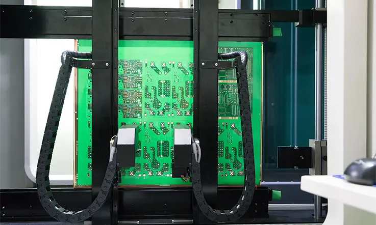
●Comprehensive in-process inspections at multiple manufacturing stages.
●Advanced final verification methods, including microsection analysis and Time Domain Reflectometry (TDR) impedance testing.
Quality Metric
Industry Standard/Method
Target Level
Fabrication Standard
IPC-6012
Class 3
Assembly Standard
IPC-A-610
Class 3
Material Traceability
ERP/QMS System
100% batch traceability
In-Process Inspection Frequency
AOI/X-ray at multiple stages
≥ 3 checkpoints
Final Verification
Microsection & TDR
±5% impedance tolerance
Transparent Pricing and Total Value
The true expense of a PCB is its total cost of ownership, not its upfront price. A valuable partner focuses on delivering reliability that prevents costly field failures. Indicators of this approach include:
●Clear, transparent pricing structures with no hidden costs.
●A focus on achieving high first-pass yields to avoid schedule delays and rework.
●The offering of a complimentary, in-depth Design for Manufacturability/Assembly (DFM/DFA) analysis before production begins to identify and resolve potential issues early.
Predictable Scheduling and Proactive Management
Time-to-market is a deciding factor in product development. A capable partner manages this through diligent oversight and clear communication. Hallmarks of this capability are:
●A single-point-of-contact project management style that ensures clear accountability.
●Proactive and consistent communication with regular status updates.
●Strong relationships with material suppliers to anticipate and mitigate material sourcing delays.
Responsive and Accessible Engineering Support
Complex projects often present technical challenges. A superior partner provides direct access to experienced engineering talent throughout the project lifecycle. This should include:
●A collaborative approach to solving difficult design issues efficiently.
●Actionable feedback on design choices from the initial quote through to final delivery.
●Technical depth that reflects a genuine understanding of advanced PCB technologies.
Verifiable Advanced Capabilities
A partner’s stated capabilities must be verifiable and aligned with the demands of specialized PCBs. This includes demonstrated proficiency with:
Q1: What is a “keep-out” zone in a rigid-flex design?
A: It’s a specified area on the flexible part of the board, especially near the transition to the rigid section, where no components, vias, or sharp trace turns should be placed. This prevents mechanical stress and potential cracking during bending.
Q2: For impedance control, is it better to adjust trace width or dielectric height?
A: It is almost always better and more practical to adjust the trace width. The dielectric height is fixed by the chosen prepreg in the board’s stack-up, while trace width can be precisely controlled during the etching process for fine-tuning.
Q3: What does “aspect ratio” mean in PCB drilling?
A: It’s the ratio of the hole’s depth to its diameter. A high aspect ratio (e.g., >10:1) is challenging because it is difficult to achieve even copper plating inside a deep, narrow hole, potentially leading to unreliable via connections.
Q4: What is “delamination” and what causes it?
A: It is the separation of layers within a PCB. It is a serious defect often caused by trapped moisture in the laminate expanding during high-temperature assembly, or by an improper lamination cycle (incorrect heat or pressure).
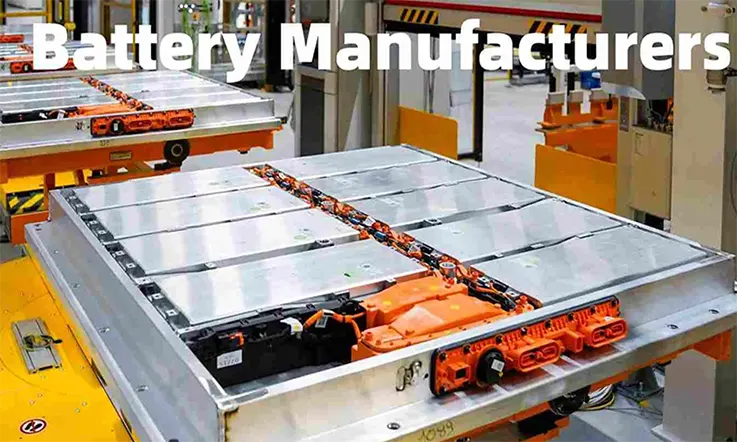
The field of modern energy storage merges two distinct disciplines: electrochemistry and electronics. The chemical composition of a battery cell defines its energy potential; the electronics governing it dictate its realized performance, safety profile, and operational lifespan. This text provides a detailed analysis of contemporary battery technologies, with a specific focus on the sophisticated Printed Circuit Board (PCB) assemblies that form the foundation of any advanced Battery Management System (BMS). It explores the design intricacies, material science, and fabrication considerations that enable the next generation of power solutions.
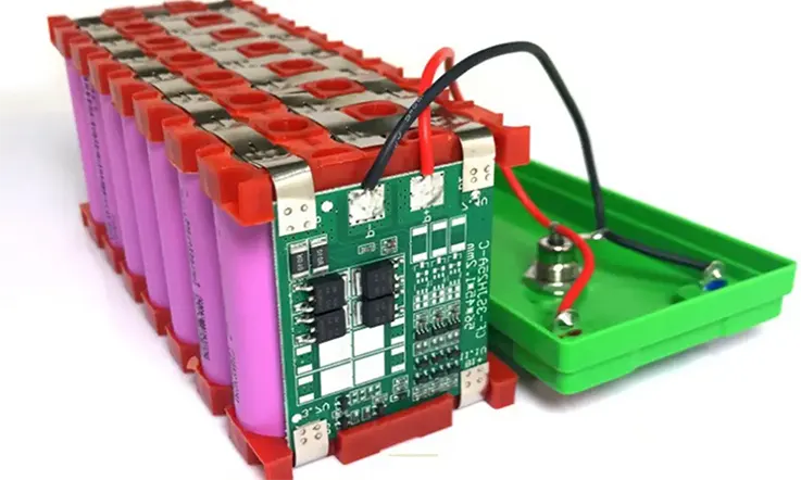
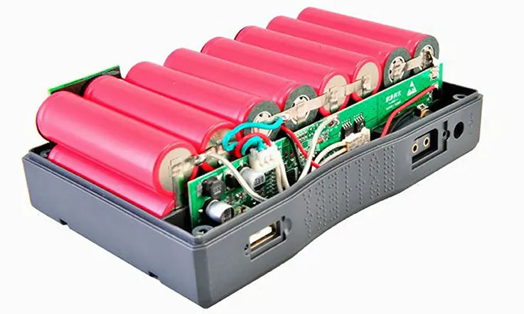
The Function of the Battery Management System (BMS)
A Battery Management System (BMS) governs the operation and performance of a battery pack. As an electronic system built upon a Printed Circuit Board (PCB), it oversees all operational aspects. A malfunction within the BMS, often stemming from the circuit board itself, can lead to the failure of the entire pack.
State of Charge (SOC) and State of Health (SOH) Estimation
The BMS calculates the battery’s available energy (State of Charge) and assesses its long-term degradation (State of Health). These determinations are derived from high-precision measurements of cell voltage, current, and temperature. The precision of these estimations is a direct consequence of the signal integrity maintained by the PCB. A well-executed board layout and fabrication process minimizes signal distortion, providing the microcontroller with accurate data.
Cell Balancing
Manufacturing variations mean that individual cells in a pack have slight differences in capacity and internal resistance. The BMS uses balancing circuits, physically located on the PCB, to equalize the charge level across all cells. This process maximizes the pack’s usable capacity and can extend its operational lifespan by 10-20%. The effectiveness of these balancing circuits is dependent on the PCB’s thermal design and component assembly.
Safety and Protection
The BMS provides a layer of protection against hazardous conditions. Its circuitry, housed on the PCB, is designed to disconnect the battery from the load or charger to prevent:
●Over-voltage and under-voltage events
●Over-current situations
●Temperatures outside of the designated operating range
The dependability of these protective measures is directly related to the manufacturing and assembly quality of the Printed Circuit Board.
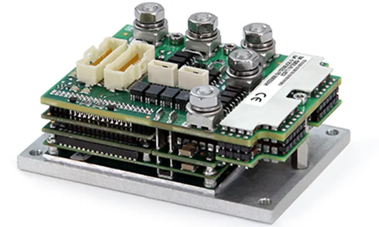
Anatomy of a High-Performance BMS PCB
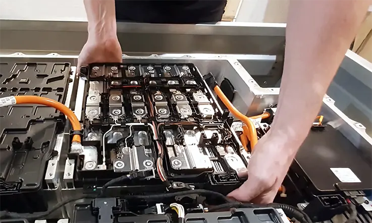
The Printed Circuit Board for a Battery Management System is a complex component, engineered to handle conflicting technical demands. It must route high-power currents while protecting sensitive, low-voltage measurement circuits, all within a compact footprint. Multi-layer constructions are the standard approach to resolving these challenges.
The board’s architecture addresses two main areas:
High-Power Circuit Management
BMS boards must manage substantial electrical loads, sometimes hundreds of amperes, which requires specific manufacturing and assembly solutions.
●Heavy Copper Traces: The manufacturing process utilizes heavy copper layers (e.g., 3oz, 4oz, or thicker) to reduce resistive heating and improve thermal dissipation.
●Embedded Busbars: For extreme current requirements, the assembly may involve embedding or soldering solid copper busbars directly onto the board, a specialized integration technique.
●Voltage Isolation: With system voltages reaching 400V or 800V, the fabrication process must ensure exacting clearance (air gaps) and creepage (surface distance) between conductors to prevent high-voltage arcing.
Parameter
Typical Value
Purpose/Impact
Copper Thickness
3oz – 6oz
Lower resistance, improved heat dissipation
Max Continuous Current
100A – 300A
Ensures reliable operation without overheating
Busbar Cross-Section
10mm² – 25mm²
Handles peak current surges without significant voltage drop
Clearance (Air Gap)
≥ 6.4 mm @ 800V
Prevents arcing between high-voltage conductors
Creepage (Surface Distance)
≥ 8 mm @ 800V
Prevents surface leakage currents in high-voltage applications
Precision Signal Path Design
The board must provide a clean environment for measuring millivolt-level signals from each battery cell, which are susceptible to electromagnetic interference (EMI).
●Signal Isolation: A multi-layer architecture allows for routing these sensitive analog traces on dedicated internal layers, physically separated from noisy, high-current paths.
●Ground Planes: The inclusion of internal ground planes creates a stable reference and a short return path for signals, shielding them from interference and preserving the accuracy of measurements.
●Controlled Impedance: This structured layering, achieved through a precise fabrication process, establishes a controlled impedance environment necessary for dependable data acquisition.
Parameter
Typical Value
Purpose/Impact
Signal Trace Width
4 – 6 mil
Reduces noise pickup while maintaining controlled impedance
Differential Pair Spacing
6 – 8 mil
Ensures balanced impedance and reduces crosstalk
Ground Plane Thickness
1oz – 2oz
Provides low-impedance return path and EMI shielding
Analog-Digital Separation
≥ 20 mm
Minimizes interference from switching circuits
Controlled Impedance Tolerance
±10%
Ensures reliable, repeatable high-speed or precision analog signal measurements
PCB Layout and its Influence on Firmware
In a BMS, the hardware and firmware are inseparable. The physical layout of the Printed Circuit Board has a direct effect on firmware operation and the efficiency of the development process. A layout that fails to account for this relationship can create significant downstream difficulties.
Key areas where the PCB layout affects firmware include:
Signal Timing and Communication
For peripherals like the Serial Peripheral Interface (SPI) that interface with an Analog Front-End (AFE), the physical length and routing of PCB traces determine signal propagation delay.
●Synchronization Issues: Mismatched trace lengths can cause data and clock signals to become misaligned, resulting in communication errors.
●Firmware Complications: These hardware-level timing issues force the firmware to compensate, often with slower clock speeds or more complex error-handling routines, reducing overall performance.
●Manufacturing Precision: Executing a layout with precisely matched trace lengths is a feature of a disciplined fabrication process that holds tight tolerances.
Accessibility for Programming and Debugging
The firmware development lifecycle depends on physical access to the microcontroller for programming and real-time diagnostics.
●Connector Placement: A thoughtful layout provides clear access to programming headers (e.g., JTAG, SWD), positioning them away from large components or mechanical housings.
●Assembly Considerations: Obstructions due to poor component placement during assembly can make connecting a debugger difficult, impeding development, testing, and field service.
Hardware Resource and Pin Assignment
The PCB routing must align with the microcontroller’s internal architecture to enable intended performance.
●Function-Specific Pins: For example, pins for high-frequency Pulse-Width Modulation (PWM) are often linked to dedicated hardware timers within the silicon.
●Enabling Hardware Acceleration: The board layout must route these signals to the correct physical pins. This allows the firmware to utilize the device’s hardware accelerators for timing-sensitive tasks, rather than resorting to less precise software-based emulation.
Therefore, the PCB is more than a substrate for components; it is an active part of the system’s computing architecture. Its design and fabrication have direct consequences on software behavior and reliability.
Battery Technology Leaders and Their PCB Demands
The following corporations are at the forefront of battery cell and system development. Their advancements in chemistry and mechanical architecture generate new demands for sophisticated electronic controls and the underlying PCB technology.
As a massive producer of electric vehicle batteries, CATL’s innovations in pack architecture directly influence the complexity of the BMS and its circuit board.
●Cell-to-Pack (CTP) Technology: This approach integrates cells directly into the pack, removing the intermediate module structure. It requires large-format or interconnected PCBs to manage signals and power across the pack’s entire area.
●Qilin Battery: This next-generation CTP design incorporates large-surface liquid cooling plates. The BMS circuit board for this system must be designed for tight mechanical and thermal integration with the cooling hardware.
BYD Company Ltd.
BYD’s vertical integration has enabled it to pioneer unique battery structures that merge energy storage with mechanical functions.
●Blade Battery: This design uses long, thin cells as structural members of the pack. The associated PCBs must also be long and narrow, capable of mounting sensors along their length to capture precise thermal and voltage data without signal degradation.
LG Energy Solution Ltd.
LG Energy Solution is a major supplier of high-energy pouch cells, particularly those with high-nickel NCM and NCMA chemistries.
●Pouch Cell Form Factor: The flexibility of pouch cells allows packs to fit non-rectangular spaces. This application often requires rigid-flex PCBs or multiple interconnected rigid boards, demanding advanced fabrication and assembly methods.
●High-Nickel Chemistry Management: These chemistries require exceptionally precise thermal and voltage control. The corresponding PCBs need to support high-sensitivity analog circuitry and fast-switching protection components, often necessitating specific material choices to manage performance.
Panasonic Corporation
Panasonic is a powerhouse in cylindrical cell production, known for mass-producing cells with remarkable uniformity for partners like Tesla.
●Cylindrical Cell Architectures (e.g., 2170, 4680): Packs built from thousands of cylindrical cells typically use a hierarchical BMS. This creates a demand for two classes of boards: compact, cost-effective slave boards produced in high volume, and a sophisticated master controller with high processing power.
●4680 Cell Format: The larger 4680 cell’s tabless design alters the pack’s thermal profile. The BMS and the sensor placement on its PCBs must be adapted to accurately monitor these new thermal dynamics.
Samsung SDI Co., Ltd.
Samsung SDI is a leading producer of prismatic cells for the EV market and is also active in small-format batteries.
●Prismatic Cells: These rectangular cells offer high packaging efficiency. Their application in EVs leads to demand for modular PCB designs that can be reliably manufactured and assembled for various scalable pack configurations.
●High-Density Applications: For compact devices, the protection circuits require high-density interconnect (HDI) PCBs, featuring microvias and fine-line manufacturing processes.
Tesla, Inc.
Tesla’s brand is built on its battery and software technology, with its in-house BMS development being a core competency.
●Advanced BMS Algorithms: Tesla’s BMS is known for its accurate predictive models. The underlying PCBs must provide an exceptionally stable, low-noise platform to support the high-speed processors running this software.
●In-House ASIC Development: Tesla develops its own Application-Specific Integrated Circuits (ASICs). This requires a PCB manufacturing partner capable of handling designs with high-density layouts that are tightly coupled with proprietary silicon.
Bridging Design and Fabrication: DFM and DFA Principles
A theoretically sound design is only practical if it can be manufactured and assembled reliably at a reasonable cost. Design for Manufacturability (DFM) and Design for Assembly (DFA) are methodologies that align a design with real-world production capabilities. Engaging with these principles early prevents costly revisions and production delays.
Key considerations in this process include:
Panelization Strategy
Individual PCBs are produced on larger master panels. An optimal panelization scheme, often developed in consultation with the fabricator, maximizes the number of boards per panel to reduce material waste and lower per-unit cost. The strategy also incorporates features for automated assembly, such as V-grooves for clean separation and fiducial marks for machine vision alignment.
Component Selection and Footprint Design
A review against DFA principles helps guide the selection of components suitable for high-speed automated assembly.
●Standard Packages: Choosing standard component packages can improve placement speed and component availability.
●IPC-Compliant Footprints: The design of the copper pads (footprints) on the PCB is a direct factor in solder joint quality. Adherence to IPC standards for footprint dimensions ensures proper solder fillet formation and prevents common assembly defects.
Test Point Strategy
A product’s reliability is verified through testing, which requires access to the circuitry. A DFM analysis identifies optimal locations for dedicated test pads on the PCB. Planning these access points from the beginning enables efficient In-Circuit Testing (ICT) and Functional Circuit Testing (FCT) after assembly, reducing the cost of quality control.
Clearances and Tolerances
Every fabrication process has inherent physical limitations. DFM analysis verifies that clearances are appropriate for the design’s voltage requirements while remaining within the fabricator’s standard process capabilities. Requesting tolerances tighter than necessary can substantially increase costs and lead times without providing additional performance benefits.
Architecting for Agility: Modular and Scalable BMS Platform Design
For organizations developing a portfolio of products, a one-off design approach is inefficient. Adopting a modular and scalable platform architecture for the BMS allows for faster development cycles, reduced development costs, and greater product line flexibility. A manufacturing partner with versatile capabilities is a prerequisite for implementing such a strategy.
Key architectural patterns include:
The Configurable Platform
This methodology involves designing a core BMS PCB that can be adapted for a family of applications. For example, a single board layout might support battery packs from 10S to 16S configurations by populating or depopulating specific Analog Front-End (AFE) chips and their associated components. This approach relies on an assembly partner with robust process control to manage multiple Bill of Materials (BOM) variants on a single layout.
Master-Slave Architecture
For very large systems, such as grid-scale energy storage, a distributed master-slave architecture is employed. This approach requires a supplier capable of producing two distinct types of circuit boards efficiently.
●Slave Units (CMUs): Numerous small, cost-optimized Cell Monitoring Unit (CMU) boards are distributed throughout the pack. Their fabrication process must be tailored for high-volume production without sacrificing measurement precision or reliability.
●Master Controller: A single, more powerful master controller aggregates data from all slave units. The PCB for this master unit is typically a complex, low-volume board with high component density, demanding advanced fabrication and assembly capabilities.
Firmware Modularity
A modular hardware platform is paired with a corresponding modular firmware architecture. The software is structured with a Hardware Abstraction Layer (HAL) that allows the core application code to function across different hardware configurations. The success of this software strategy is predicated on the hardware being assembled with perfect fidelity to the design, ensuring the HAL interacts with a predictable and dependable physical layer.
Strategic Substrate Selection for BMS PCB Reliability
The choice of a PCB’s base material is an engineering decision that governs its thermal, electrical, and mechanical performance. This selection has a direct bearing on the final product’s reliability and cost. Different BMS applications demand different substrate properties.
FR-4: The Industry Standard
Flame Retardant 4 is a glass-reinforced epoxy laminate. It is the most common PCB substrate, offering a well-balanced profile of mechanical strength, electrical insulation, and cost-effectiveness for a wide range of applications.
Parameter
Typical Value
Dielectric Constant (Dk)
4.2 – 4.8
Glass Transition Temp (Tg)
130°C – 140°C
Thermal Conductivity
0.3 – 0.4 W/m·K
Volume Resistivity
10¹⁰ – 10¹² Ω·cm
Cost Level
Low
High-Tg FR-4 for Elevated Temperatures
In applications with higher ambient or operating temperatures, such as in enclosed battery packs, High-Tg FR-4 is specified. With a glass transition temperature (Tg) of 170-180°C, this material maintains its structural integrity and performance where standard FR-4 would degrade.
Parameter
Typical Value
Dielectric Constant (Dk)
4.2 – 4.5
Glass Transition Temp (Tg)
170°C – 180°C
Thermal Conductivity
0.3 – 0.4 W/m·K
Coefficient of Thermal Expansion (CTE)
55–65 ppm/°C
Cost Level
Medium
IMS for Thermal Management
For dissipating large amounts of heat from power components, an Insulated Metal Substrate (IMS) board is a superior choice. Built on an aluminum or copper base, an IMS board’s fabrication process results in thermal conductivity that can be over 100 times greater than FR-4. A properly designed IMS board can lower a component’s operating temperature by 20-30°C.
Parameter
Typical Value
Thermal Conductivity
1.0 – 3.0 W/m·K (dielectric layer)
Base Material
Aluminum (1–3 mm) / Copper (1–2 mm)
Dielectric Breakdown Voltage
≥ 3 kV
Operating Temp Range
-40°C to +150°C
Cost Level
Medium to High
High-Frequency Materials for Wireless BMS
The emergence of wireless BMS (wBMS) requires materials suitable for RF signals. Substrates from suppliers like Rogers Corporation offer low dielectric constants (Dk) and dissipation factors (Df). Fabricating boards with these materials requires specialized handling to preserve the properties needed for efficient antenna performance and reliable data transmission.
Parameter
Typical Value
Dielectric Constant (Dk)
2.2 – 3.5
Dissipation Factor (Df)
0.0005 – 0.002
Operating Frequency Range
Up to 40 GHz
Thermal Conductivity
0.6 – 1.0 W/m·K
Cost Level
High
Ceramic Substrates for Extreme Environments
For the most demanding applications with extreme temperatures or very high voltages, ceramic substrates such as Alumina (Al₂O₃) or Aluminum Nitride (AlN) are employed. They provide exceptional thermal conductivity and high-voltage insulation, but their fabrication is more complex and costly than conventional PCB materials.
Parameter
Alumina (Al₂O₃)
Aluminum Nitride (AlN)
Thermal Conductivity
20 – 30 W/m·K
140 – 180 W/m·K
Dielectric Strength
≥ 10 kV/mm
≥ 12 kV/mm
Coefficient of Thermal Expansion (CTE)
6 – 8 ppm/°C
4 – 5 ppm/°C
Operating Temp Range
-55°C to +300°C
-55°C to +300°C
Cost Level
High
Very High
Advanced Thermal Management Strategies for Power-Dense PCBs
Heat degrades the performance of both battery cells and the electronics that manage them. Effective thermal management at the PCB level is a core design discipline that combines thoughtful layout with advanced fabrication and assembly techniques.
Heavy Copper and Busbars
The first line of defense against heat is to minimize its generation at the source. The fabrication of a PCB with heavy copper traces (e.g., 3oz, 4oz, or thicker) for high-current paths lowers their electrical resistance (I²R), directly reducing resistive heat loss. For extreme currents, solid copper busbars can be integrated during the assembly process.
Thermal Vias for Heat Extraction
To conduct heat away from a surface-mount component, an array of thermal vias is designed into its underlying thermal pad.
●Heat Conduction: These plated-through holes act as conductive channels, transferring thermal energy from the top layer to internal or bottom copper planes.
●Fabrication Process: The manufacturing process can include filling these vias with conductive epoxy to maximize heat transfer and capping them with copper. This via-in-pad process creates a flat, reliable surface for soldering the component.
Heat Sink Integration
When on-board heat spreading is insufficient, an external heat sink is added. This is an assembly-centric process.
●Thermal Interface: It involves the precise application of a Thermal Interface Material (TIM) to eliminate air gaps between the component and the heat sink.
●Mechanical Assembly: The process requires applying a specified mounting pressure to ensure an efficient and dependable thermal connection.
Liquid Cooling Integration
In the most demanding high-performance systems, direct liquid cooling is employed. This solution requires a precise mechanical assembly process to mount the BMS PCB to a liquid-cooled “cold plate,” ensuring uniform contact and maximum heat transfer from the board to the flowing coolant.
Navigating the Volatile Supply Chain: Component Sourcing and Lifecycle Management
The integrity of a BMS is founded upon the authenticity and availability of its electronic components. Navigating the modern electronics supply chain presents substantial challenges. A partnership with an experienced manufacturing and assembly provider is a direct approach to mitigating these risks.
Key aspects include:
Sourcing of Qualified Components
BMS for automotive or industrial applications require components that meet stringent qualification standards, such as AEC-Q100 for integrated circuits. These parts often have long lead times. An assembly partner with established supplier relationships can provide visibility into market conditions and help manage procurement schedules to align with a project’s timeline.
Counterfeit Component Mitigation
The use of counterfeit components, often sourced from unauthorized channels, poses a severe safety hazard that can lead to catastrophic failure of BMS protection systems. Partnering with an assembler that maintains a rigorously vetted, secure supply chain with traceable parts is the most effective way to eliminate this risk.
Resilient Design Through Alternate Parts
To guard against supply chain disruptions, a resilient design strategy includes identifying pin-compatible alternate components from different suppliers. A knowledgeable assembly partner can support this effort by leveraging their procurement data to recommend viable alternates during the initial design phase, providing flexibility without requiring a board redesign.
Component Lifecycle Management
Electronic components have a finite production life. For products with long service durations, such as industrial equipment, End-of-Life (EOL) notices for components must be monitored. An assembly partner can offer component lifecycle tracking as a service, providing early warnings for EOL parts to allow for strategic “last-time buys” or planned transitions to next-generation designs.
Securing the Core: Cybersecurity Considerations for Connected BMS Designs
As BMS technology becomes more connected through wireless interfaces and vehicle networks, it also becomes a potential target for malicious attacks. Securing the BMS is now a fundamental aspect of the overall system design, encompassing the silicon, the software, and the physical circuit board itself.
Understanding Attack Vectors
A connected BMS can be targeted through various entry points on the PCB. The CAN bus port, common in vehicles, can be susceptible to message spoofing. A wireless BMS (wBMS) could be targeted via its radio interface and antenna traces. A successful attack could falsify sensor readings, disable safety features, or render a battery pack inoperable.
Hardware-Based Security
Modern microcontrollers often include a Hardware Security Module (HSM)—a dedicated, tamper-resistant coprocessor that handles cryptographic operations.
●Secure Boot: Using an HSM for functions like secure boot verifies the authenticity of the firmware at startup, preventing unauthorized software from running on the BMS.
●Component Authenticity: The security offered by an HSM is predicated on sourcing authentic components. A counterfeit security chip, acquired through an unsecured supply chain, provides no actual protection.
Physical PCB Security Measures
The physical PCB layout and assembly process must reinforce security.
●Debug Port Protection: In production units, debug ports (like JTAG or SWD) can be disabled during assembly by not populating the physical headers or by covering their pads, restricting unauthorized physical access.
●Internal Trace Routing: Routing traces that carry sensitive information on internal layers of the PCB makes physical probing and reverse-engineering substantially more difficult and costly for an attacker.
●Manufacturing Integrity: A secure design can be compromised if fabricated at an untrusted facility. Partnering with a manufacturer that has secure data handling policies is a measure to protect intellectual property and prevent the introduction of hardware backdoors.
The Path to Zero Defects: Advanced Quality Assurance Methodologies
Achieving high reliability in a BMS PCBA is not the result of final testing alone; it is the outcome of a systemic approach to quality embedded throughout the fabrication and assembly process.
In-Process Inspection for Defect Detection
●Automated Optical Inspection (AOI): Following assembly, our process utilizes AOI, where high-resolution cameras inspect 100% of PCBAs for defects like component misalignment, insufficient solder, or solder bridges.
●Automated X-ray Inspection (AXI): For components with hidden solder joints, such as Ball Grid Arrays (BGAs), we employ AXI to see through the component package and verify the structural integrity of each connection.
Adherence to IPC Reliability Standards
●IPC Class 2: This is the accepted standard for general commercial and industrial electronics.
●IPC Class 3: For applications where failure is not a tolerable outcome—such as automotive safety systems, medical life support, or aerospace—we have the process controls and verification methods to manufacture and assemble boards that comply with the rigorous requirements of IPC Class 3. This includes stricter tolerances, complete vertical fill of plated through-holes, and more robust annular ring specifications.
Systematic Process Control for Defect Prevention
●Statistical Process Control (SPC): Beyond simply detecting defects, our fabrication process incorporates SPC to monitor process variables in real-time. By analyzing trends, we can adjust parameters before they deviate out of specification, preventing defects from occurring.
●Component-Level Traceability: We provide full traceability by assigning a unique serial number to each PCBA. This number links the finished board to the specific batches of materials, components, machines, and operators involved in its creation. In the event of a field anomaly, this data enables a precise root cause analysis.
Navigating Global Markets: Compliance and Certification Standards
A product’s market access depends on its conformity to the regulations of the regions where it will be sold. For a BMS, achieving compliance is a mandatory step where the manufacturing and assembly process plays a foundational part.
ISO 26262 for Functional Safety
This is the governing standard for functional safety in road vehicles, establishing Automotive Safety Integrity Levels (ASIL).
●Design Implications: A BMS in a passenger vehicle often requires a high ASIL rating, mandating design features like redundant microcontrollers and diversified power supplies, which increases PCB complexity.
●Manufacturing Correlation: Achieving high ASIL ratings is supported by manufacturing to the highest reliability standards, such as IPC Class 3, to ensure the physical durability of these safety mechanisms.
H3:UL Certification for Safety
Underwriters Laboratories (UL) standards are a benchmark for product safety, particularly in the North American market.
●Material Compliance: Our fabrication process utilizes substrate materials that meet the UL 94 flammability standard, typically with a V-0 rating.
●Process Traceability: We maintain robust process controls and documentation, which can support a client’s efforts to certify their end-product to standards like UL 2580 (Batteries for Use In Electric Vehicles).
IEC Standards for Global Benchmarking
The International Electrotechnical Commission (IEC) provides globally recognized standards that facilitate international trade. Our production and quality management practices are aligned with the principles outlined in benchmarks like IEC 62133 (safety requirements for portable sealed secondary cells).
Environmental Regulations: RoHS & REACH
These European regulations, which restrict specific hazardous materials, have become de facto global standards. Our procurement process is managed to ensure that all components and raw materials used in our assembly—from solder paste to PCB finishes—are compliant with RoHS and REACH directives.
Beyond Per-Unit Price: Analyzing the Total Cost of Ownership (TCO) for BMS PCBs
A comprehensive evaluation of a BMS solution extends beyond its initial purchase price. The Total Cost of Ownership (TCO) provides a more complete financial picture, accounting for all costs incurred throughout the product’s lifecycle. A lower per-unit price on a PCBA can often lead to significantly higher long-term expenditures.
The Cost of Field Failures
A single BMS failure in a deployed system can have astronomical financial consequences. For an electric vehicle, this could trigger a product recall costing millions. In a grid storage application, a failure could lead to service outages with severe contractual penalties. These potential costs dwarf any initial savings from a lower-cost component. This risk is directly addressed by manufacturing to high-reliability standards, such as IPC Class 3, and verified through the advanced QA methodologies detailed previously.
The Hidden Costs of Inefficient Manufacturing
A design that is not optimized for manufacturability can result in lower production yields and complex assembly issues that consume valuable engineering time. A 5% yield loss effectively increases the cost of every good unit. This underscores the financial benefit of the collaborative DFM and DFA review process, which eliminates many of these potential problems before production ever begins.
The Cost of an Inflexible Supply Chain
A design locked into a single-source component that faces a supply disruption can halt an entire production line. The cost of this downtime, in lost revenue and fixed operational expenses, can be immense. For this reason, procurement support that includes identifying and validating alternate components is a form of insurance against these substantial supply chain risks.
The Value of Long-Term Reliability
The TCO analysis reveals that choosing a high-quality, robustly designed, and thoroughly tested PCBA is not an expense, but a risk mitigation strategy. A greater initial investment in a resilient design and a high-reliability manufacturing process directly reduces the probability of incurring much larger downstream costs associated with failures, rework, and operational disruptions. It is an investment in the product’s performance, its brand’s reputation, and its overall commercial success.
Case Study: High-Density BMS for a Light Electric Vehicle (LEV)
This case study illustrates the application of advanced design and manufacturing principles to solve a challenging real-world problem.
The Challenge A client required a compact and robust BMS for a high-performance electric scooter. The system needed to manage a 14S (58.8V) battery pack capable of delivering a 50A continuous discharge current. The primary constraint was the severe space limitation: the entire PCBA had to fit within a narrow 60mm x 220mm footprint inside the scooter’s deck, an environment subject to constant vibration and potential moisture exposure.
The Solution:A multi-faceted approach was taken to meet all performance, size, and reliability requirements.
High-Density PCB Design
●8-Layer Construction: An 8-layer PCB was engineered to accommodate the high routing density in such a limited area. This included dedicated internal ground and power planes to ensure signal integrity.
●Heavy Copper for High-Current Path: Two internal layers were fabricated with 4oz heavy copper to handle the 50A continuous current while minimizing heat generation.
Advanced Thermal Management
To manage the ~25W of waste heat from the power stage within the enclosed space, a hybrid thermal solution was developed.
●Integrated Aluminum Core: A section of the FR-4 board was manufactured with an integrated aluminum core directly beneath the high-power MOSFETs.
●High-Density Thermal Vias: An array of 150 thermal vias was designed into the MOSFETs’ thermal pads, efficiently channeling heat to the aluminum core. This core was then thermally coupled to the scooter’s main aluminum frame, turning the vehicle’s structure into a functional heat sink.
Design for Manufacturing and Test (DFM/DFT)
To ensure a smooth transition from design to high-yield production, several DFM and DFT principles were applied.
●Optimized Panel Layout: The board was panelized to fit 6 units per production panel, using V-grooves for clean, stress-free separation after assembly.
●Accessible Test Points: All necessary test points for the automated functional test sequence were consolidated on one side of the board for efficient testing.
Assured Reliability
The final deliverable was a fully assembled and tested PCBA, built for long-term durability in a harsh environment.
●IPC Class 3 Fabrication: The board was manufactured and assembled to the high-reliability IPC Class 3 standard.
●Conformal Coating: After functional testing, each board was treated with a UL-certified acrylic conformal coating to protect the electronics from moisture and debris.
Frequently Asked Questions (FAQ) about Battery PCBs
Q: What is the most common Design for Manufacturability (DFM) issue found in BMS PCB designs?
A: A frequent issue is insufficient spacing between high-voltage areas and low-voltage signal circuits, along with inadequate copper width for high-current paths, which can affect both safety and thermal performance.
Q: Are there specific design recommendations for the pads that connect directly to battery cells?
A: It is recommended to use large, non-circular pads (e.g., rectangular or U-shaped) with multiple vias. This increases the mechanical strength of the solder joint and enhances current-carrying capacity, preventing failure under vibration or high current loads.
Q: What is impedance control, and when is it needed for a BMS PCB?
A: Impedance control is a manufacturing process that ensures a specific trace on a PCB has a defined electrical characteristic. For a BMS with high-speed communication interfaces (like CAN, Ethernet) or wireless functions (wBMS), impedance control is applied to the relevant signal lines to maintain signal integrity.
Q: What are the primary factors that affect the lead time of a BMS PCBA order?
A: The main factors include: the layer count and complexity of the bare PCB, the presence of long-lead-time components in the Bill of Materials (BOM), the order quantity, and any required certification testing.
Evaluation Criteria for a High-Reliability PCB Assembly Specialist
Selecting the right fabrication and assembly specialist is a decision that directly influences a project’s outcome. The evaluation should extend beyond a simple price quotation and encompass a holistic view of capability, quality, and service. The following attributes define a top-tier specialist for battery system electronics.
Demonstrable Quality Systems
A specialist’s commitment to quality is evident not in claims, but in their certified systems.
●Holds high-level quality management certifications, such as ISO 9001, and market-specific credentials like IATF 16949 for automotive applications.
●Possesses the process controls and verification methods to manufacture and assemble products compliant with the high-reliability IPC Class 3 standard.
●Employs advanced quality methodologies, including component-level traceability and Statistical Process Control (SPC) for defect prevention.
Value-Oriented Pricing through Total Cost of Ownership (TCO)
The lowest initial price rarely equates to the lowest long-term cost. A strategic specialist discusses pricing in the context of TCO.
●Demonstrates how expertise in DFM, process control, and counterfeit prevention reduces the risk of costly field failures, recalls, and production delays.
●Delivers value by manufacturing a reliable product that functions correctly for its entire intended lifespan.
●Protects the client’s brand reputation by preventing immense downstream costs associated with poor quality.
Reliable and Transparent Delivery
Consistent on-time delivery is a function of operational excellence.
●Provides clear and realistic lead-time estimates based on sophisticated production scheduling.
●Maintains proactive supply chain management with a network of vetted, reliable suppliers.
●Upholds open and transparent communication regarding project status and any potential disruptions.
Collaborative Engineering Service
A specialist should function as an extension of the client’s own team.
●Offers expert pre-production consultations (DFM/DFA) to optimize a design for manufacturability, cost, and reliability.
●Provides accessible and responsive engineering support to resolve technical queries throughout the production cycle.
●Fosters a collaborative partnership aimed at mutual success.
Advanced Manufacturing Capabilities
The specialist’s facility and equipment must be capable of handling the specific technical demands of modern BMS designs.
●The capacity to process a wide range of substrate materials, from high-Tg FR-4 to IMS, high-frequency RF, and ceramic substrates.
●Proven expertise in fabricating complex structures, such as high-layer-count or High-Density Interconnect (HDI) boards, often with heavy copper features.
●Utilizes modern automated systems for Surface Mount Technology (SMT), 3D X-ray Inspection (AXI), and conformal coating application.
Printed circuit boards (PCBs) form the operational platforms for nearly all modern electronic devices. Among the substrate materials used in their construction, fiberglass composites, especially FR-4, are widely employed. This leads to fundamental questions: What precisely defines a Fiberglass PCB, and what attributes account for its extensive application in PCB Manufacturing?
This document addresses these inquiries through a detailed exploration of Fiberglass PCB technology. We will examine Fiberglass PCB materials, including FR-4 and its properties, and categorize the various Fiberglass PCB types. The discussion will cover Fiberglass PCB design considerations, the intricacies of the Fiberglass PCB manufacturing lifecycle—from fabrication to assembly and finishing—and aspects of quality assurance and reliability.
Defining Fiberglass PCB: The Foundational Substrate
Fiberglass PCBs form the workhorse platform for countless electronic devices. Understanding their core, especially the widely used FR-4 material, is the first step towards successful product development. This section explores not just what these materials are, but how their properties influence design and, directly, how we leverage them in our manufacturing and assembly services to benefit your project.
Unveiling Fiberglass PCB Materials: The Core Composition
Consider a Fiberglass PCB as a precisely structured composite, not merely a single element. It is a blend where different materials unite, each contributing to the creation of a sturdy, dependable base for electronic components. Appreciating this structure helps in understanding how these boards operate and how our processes ensure their integrity.
●What is Fiberglass PCB?: Uncovering the Basics?
A Fiberglass PCB is a circuit board where the insulating base is constructed from sheets of Woven Fiberglass fabric thoroughly impregnated with an Epoxy Resin binder. This Glass Fiber PCB material provides both structural support and electrical isolation. It forms the surface upon which conductive copper pathways are etched. Its favorable combination of mechanical strength, electrical performance, and manufacturing cost makes it a standard selection for a vast range of electronic applications – a combination that we expertly handle in our production.
The “Woven Fiberglass” component is a fabric-like material, providing strength and dimensional stability. This fabric is infused with an “Epoxy Resin,” a thermosetting polymer that hardens upon curing, acting as a binder and insulator. This process creates a solid Epoxy Resin PCB. When fiberglass provides the reinforcement, Glass Fiber PCB or Glass Epoxy PCB are the specific descriptors for these widely manufactured boards.
Introducing FR-4: The Industry Standard Fiberglass PCB Material
FR-4 is the most widely recognized material within the Fiberglass PCB landscape. You will frequently encounter it. Its widespread use stems from its practical, well-rounded set of capabilities that meets broad industry needs – needs that we have addressed for countless clients over many years.
●Understanding FR-4 Material & FR-4 Glass Epoxy
FR-4 Material signifies “Flame Retardant 4”. The “FR” indicates its self-extinguishing characteristic, a safety feature. The “4” represents a grade defined by NEMA. It is a specific type of FR-4 Glass Epoxy, utilizing woven glass and an epoxy system formulated to meet fire safety standards. It provides solid strength with manageable weight and reliable electrical insulation.
●Why FR-4 is the Preferred PCB Substrate Explained?
Why is FR-4 so common? The PCB Substrate Explained simply: it offers an advantageous cost-to-performance ratio. It provides dependable electrical separation, handles heat adequately for numerous applications, possesses good physical strength, and its well-established manufacturing processes make it reasonably priced. This combination makes it a frequently selected PCB substrate, and its familiarity allows our production lines to operate with high efficiency, translating into reliable delivery and cost advantages for your projects.
Key Fiberglass PCB Materials Properties: Performance Deep Dive
Understanding its composition leads to appreciating its performance. These FR-4 Material Properties directly influence circuit behavior and manufacturability. This is where material science meets practical application – and where our expertise adds value.
Electrically, FR-4 functions as an effective insulator – its PCB Insulation qualities prevent current from flowing in unintended paths. Design specialists closely monitor the Dielectric Constant (Dk), as this value affects signal propagation speed and impedance control. While FR-4’s Dk offers a degree of predictability, managing its variations with frequency requires careful consideration during high-speed design – a challenge our team can help you navigate.
●Mechanical Properties: High Strength, Durability & Dimensional Stability
These boards possess considerable physical resilience. They exhibit High Strength PCB features, resisting bending and impacts. This Durability means boards built by our expert assembly teams can withstand handling and operational demands. Furthermore, their Dimensional Stability ensures they maintain their form across temperature variations, contributing to a longer product lifespan and reliable device operation.
●Thermal Properties & Flame Retardant PCB Safety
Standard FR-4 manages typical operational temperatures and soldering without issue for many devices. While not designed for extreme high-temperature environments, it is sufficient for many uses. Its Flame Retardant PCB Safety (typically meeting UL 94V-0) is a pronounced benefit, contributing to product safety across many industries – a compliance aspect we ensure in our certified processes.
Exploring Fiberglass PCB Types: A Comprehensive Overview
Fiberglass PCBs offer a spectrum of solutions, moving beyond a single, uniform approach. Different electronic applications present unique demands, which are met by a diverse range of board configurations. Understanding these Fiberglass PCB types is a foundational step in selecting an appropriate platform for any electronic project to meet its performance requirements. This section outlines the different categories to provide clarity on the available options.
Classifying Fiberglass PCB Types by Layer Count
A primary method for categorizing these boards involves their number of conductive copper layers. This count directly corresponds to the complexity of the circuits they can accommodate. An increased number of layers provides greater space for routing, facilitating more compact and intricate designs.
PCB Type
Layers
Cost
Design Complexity
Common Applications
Single-Sided
1
Low
Low
Toys, power supplies, simple gadgets
Double-Sided
2
Moderate
Moderate
Consumer electronics, control systems
Multi-Layer (4+)
4 – 40+
High
High
Servers, medical devices, telecom systems
●Single-Sided PCB / Single Layer PCB: Simple & Cost-Effective
The most fundamental form is the Single-Sided PCB or Single Layer PCB. It features copper pathways on only one side of the substrate. These boards are generally inexpensive to produce and straightforward to design, frequently found in applications with lower complexity where cost considerations are a large factor. They provide a functional solution for basic electronic tasks.
●Double-Sided PCB / Double Layer PCB: Versatility & Density
For increased capability, the Double-Sided PCB or Double Layer PCB presents a solution. Featuring copper on both sides interconnected by vias (plated-through holes), this type offers significantly more area for routing traces and placing components. This enhanced density and versatility make them suitable for a wide spectrum of electronic devices.
●Multi-Layer PCB: For Complex & High-Performance Designs
For advanced applications, the Multi-Layer PCB is utilized. These boards integrate multiple double-sided layers, bonded together, creating a three-dimensional structure for highly complex circuits. With four or substantially more layers, these boards support demanding high-performance designs, such as those in servers, advanced telecommunications equipment, or medical technology, allowing for high functionality within a limited area.
Understanding Fiberglass PCB Types by Rigidity & Structure
Beyond layer count, the physical characteristics, specifically rigidity, define another set of board categories. While the majority are rigid, certain applications necessitate flexibility or a combination of rigid and flexible sections, leading to different structural approaches.
●Rigid Fiberglass PCB & Rigid Circuit Board Construction
The most common form is the Rigid Fiberglass PCB. It is stiff and provides a stable platform for components. The Rigid Circuit Board Construction, typically using standard FR-4, represents the majority of boards manufactured and serves as the standard, reliable choice for applications where the board remains stationary.
Certain applications require creative structural solutions. Flexible & Rigid-Flex PCB Possibilities allow circuits to be installed in confined spaces, connect parts that move relative to each other, or form three-dimensional assemblies. While flexible circuits often use polyimide, rigid-flex designs frequently combine FR-4 sections with flexible interconnects, offering a blend of stability and bendability, usually at a different cost point.
●High-Density Interconnect (HDI) as Advanced Fiberglass PCB Types
High-Density Interconnect (HDI) boards represent Advanced Fiberglass PCB Types. These utilize fabrication techniques such as microvias, very fine lines and spaces, and sequential lamination to achieve exceptionally high circuit density. They are a requirement for miniaturized modern devices and signify a progression in technology.
Standard configurations are not always sufficient. Specific applications present unique challenges that necessitate specialized board designs, often based on fiberglass principles but modified for particular performance characteristics.
Applications involving radio frequencies or high-speed digital signals present a distinct set of challenges. A High-Frequency PCB requires materials with specific dielectric properties (low Dk and Df). While specialized substrates are available, careful Fiberglass PCB design and the use of certain advanced FR-4 grades can be an effective approach, especially when managing production costs.
●Heavy Copper PCBs: Power & Thermal Types
When managing substantial electrical currents or dissipating significant amounts of heat is necessary, Heavy Copper PCBs are employed. These boards are enhanced with thicker copper layers on an FR-4 base. These Power & Thermal Types are used in power conversion, motor control, and automotive systems where standard boards would not suffice.
●An Introduction to Alternative Fiberglass PCB Types
While FR-4 is prevalent, it is useful to have an Introduction to Alternative Fiberglass PCB Types. Other fiberglass-based composites exist, offering variations in thermal performance or mechanical strength. These alternatives provide designers with additional options to configure a board precisely for its intended operational environment.
The ‘Why’ Behind It: Fiberglass in PCB Manufacturing
After examining the composition and varieties of these circuit boards, a central question surfaces: What makes fiberglass the prevalent choice? Given the array of available materials, the widespread preference for this glass-epoxy composite in Fiberglass PCB manufacturing warrants exploration. Its extensive use is not a matter of chance but is rooted in discernible, functional attributes. This segment delves into these attributes, clarifying the real-world advantages and the way this material’s characteristics facilitate the creation of dependable electronic assemblies that are integral to modern life.
Fiberglass PCB Manufacturing: The Advantages Unpacked
When design specialists and production supervisors assess substrate options, fiberglass often stands out as a highly suitable selection. It offers a suite of beneficial properties that are compelling, contributing to streamlined production workflows and the realization of high-caliber end-products. Its use facilitates the achievement of dependable outcomes via established fabrication techniques.
●Key Benefits of Fiberglass PCB: Strength, Insulation, Cost-Effectiveness
This substrate material provides a compelling union of three distinct merits. Firstly, its Strength: the interwoven glass filaments impart considerable physical resilience, enabling the board to withstand mechanical stresses without fracturing or deforming. Secondly, its Insulation: the epoxy binder forms an effective dielectric barrier, directing electrical current flow along intended paths and preventing unintended shorts. Thirdly, its Cost-Effectiveness: the level of performance it offers is achievable at a production expenditure that aligns with broad market requirements, making the Advantages of Fiberglass PCB persuasive for a multitude of projects.
●Why It’s the Go-To Choice for Electronics Manufacturing
This collection of traits clarifies Why It’s the Go-To Choice for Electronics Manufacturing. Professionals throughout the industry appreciate its adaptability in processing – it can be drilled, machined, and soldered with predictable results. Product developers benefit from its well-documented performance envelope. For a Fiberglass PCB manufacturer, the capacity to generate large quantities with reliable outcomes underpins a responsive supply chain. Its frequent selection is thus founded on these substantial merits.
●Comparing Fiberglass vs. Other Materials in PCB Manufacturing
While other substrate materials are available, Comparing Fiberglass vs. Other Materials frequently underscores its well-rounded characteristics. Some alternatives might present lower initial material costs but may not offer comparable mechanical robustness. Others could yield superior thermal conduction but involve increased expenditure and more complex processing. FR-4 commonly provides a versatile foundation, satisfying a wide array of needs within PCB Manufacturing. For applications with extreme high-frequency or thermal demands, alternative substrates may be explored, and material specialists can provide guidance on FR-4’s suitability or the selection of alternatives like Rogers materials or metal-core PCBs.
How Fiberglass Enhances PCB Reliability and Durability?
Initial functionality upon assembly is one aspect of performance; sustained operation throughout a device’s expected service duration, often under diverse conditions, is another. Fiberglass makes a substantial contribution to a circuit board’s capacity to endure operational challenges, leading to more robust and dependable electronic products.
●Ensuring PCB Reliability through Material Choice
The pursuit of PCB Reliability is fundamentally linked to the selection of the base substrate. Fiberglass furnishes a stable structural base that resists dimensional changes, fractures, or degradation under typical operational parameters. Its comparatively low moisture uptake, relative to some other dielectrics, helps preserve stable electrical characteristics over time, which supports predictable device operation. Controlled manufacturing environments further ensure this stability translates directly into trustworthy device performance.
●Mechanical Support PCB & Resistance to Physical Stress
Functioning as a Mechanical Support PCB, fiberglass demonstrates commendable performance. It provides the necessary rigidity to securely hold electronic components, including those of greater mass. It offers effective Resistance to Physical Stress, such as shocks encountered during product handling or vibrations experienced in operational settings, thereby protecting the delicate copper conductive patterns. Circuit boards are often structured to endure these common real-world forces.
●Long-Term Performance in Various Environments
These circuit board structures are developed for enduring service. The cured epoxy resin component exhibits resistance to a wide array of common chemicals. They preserve their structural integrity and electrical behavior across a functional temperature spectrum, facilitating Long-Term Performance in varied settings, from controlled office atmospheres to more demanding industrial locations. Protective measures like conformal coating, a service offered by fabricators, can further enhance this durability in specific challenging environments.
The Manufacturing Process: Leveraging Fiberglass Properties
The practical utility of fiberglass is also evident in its compatibility with established manufacturing workflows. Its inherent physical and chemical nature aligns well with the precise and often intricate steps involved in transforming a digital circuit design into a tangible physical object.
●How Fiberglass PCB is Made: An Overview
A review of How Fiberglass PCB is Made underscores its process adaptability. The sequence typically commences with Copper Clad Laminate (CCL) panels. These panels undergo imaging to define the circuit, etching to remove unwanted copper, drilling for vias and component mounting, plating to create conductive interconnections, and lamination to bond multiple layers in multi-layer constructions. The dimensional stability of the fiberglass base throughout these operations allows for the high degree of precision needed for fine-featured patterns, a level of exactitude that modern automated equipment reliably achieves in proficient facilities.
●The PCB Lamination Process & Copper Clad Laminate (CCL)
In the fabrication of multi-layer circuit boards, The PCB Lamination Process serves to fuse the individual layers into a cohesive structure. Sheets of etched inner-layer Copper Clad Laminate (CCL) are carefully arranged with layers of ‘prepreg’ (fiberglass cloth partially saturated with epoxy resin). This assembly is then subjected to carefully controlled cycles of heat and pressure, causing the prepreg to liquefy, flow, and cure, thus bonding the stack. The inherent properties of fiberglass facilitate the precise alignment required during this demanding stage, a process managed with exacting control using multi-stage presses and often verified with automated optical systems in well-equipped plants.
●Etching Process PCB & Circuit Formation
The Etching Process PCB is a selective copper removal technique used to define the conductive pathways. A patterned protective layer shields the desired copper circuitry while a chemical solution dissolves the exposed, unwanted copper. Meticulous control over this step ensures the formation of sharply defined conductive tracks and pads. Achieving accurate results at this juncture enables the intended electrical functionality of the circuit, an outcome delivered with high yield by advanced chemical lines at proficient manufacturing sites.
Fiberglass PCB Design: Structuring for Success
While familiarity with materials and board configurations provides an initial understanding, the actual creation of functional electronic pathways occurs during the Fiberglass PCB Design phase. This activity extends beyond mere electrical point-to-point connections; it is the art of architecting electronic systems. Those specializing in this field apply their knowledge, navigating the interplay of physical principles, manufacturing limitations, and project aims. A competently developed design operates as intended, can be produced without excessive difficulty, and aligns with fiscal expectations for production. This segment illuminates the elemental aspects of developing these fiberglass-based platforms, and clarifies how collaboration with a seasoned manufacturing entity can help transition a thoughtfully structured design into a high-performing physical circuit board.
Core Principles of Fiberglass PCB Design
Attaining favorable results with intricate designs necessitates a firm grasp of fundamental approaches. These core practices are the underpinnings for developing dependable, manufacturable circuit boards. Observance of these practices from a project’s outset helps avert later complications.
Design Aspect
Recommended Practice
Benefit
Trace Width & Spacing
Follow IPC-2221 standards
Reliable signal and power transmission
Via Types
Use appropriately sized and placed vias
Avoids manufacturing defects
Component Placement
Maintain sufficient clearance and logical layout
Enhances assembly and minimizes rework
Layer Stack Planning
Define early, including ground/power planes
Supports EMI control and power integrity
●Circuit Board Design Guidelines for FR-4
Application of recognized Circuit Board Design Guidelines for FR-4 is a customary part of product development. These directives outline specifications such as minimum conductor widths and separations, via hole attributes, and component placement clearances. Following such parameters facilitates efficient fabrication processes. Comprehensive guidelines, often refined from considerable manufacturing exposure, assist in preparing FR-4 board layouts for streamlined production from the initial design stages.
●Fiberglass PCB Design: Balancing Performance and Cost
A central consideration in Fiberglass PCB Design involves Balancing Performance and Cost. Technical specialists work to meet operational benchmarks for elements like signal velocity or power distribution capacity, while concurrently managing the overall PCB Cost. Choices related to layer count, trace pathway geometries, and material grades directly influence the final expense of production. Effective development work finds a suitable equilibrium between these elements. Technical teams at manufacturing operations often engage with clients to explore these variables, seeking an advantageous reconciliation of performance objectives and budgetary frameworks.
●PCB Stackup Design & Its Influence
The PCB Stackup Design functions as the internal constructional map for a multi-layered circuit board. It delineates the sequence and properties of copper conductive layers and FR-4 insulating strata (comprising cores and prepregs). This layered arrangement has a pronounced Influence on impedance characteristics, signal transmission quality, electromagnetic compatibility (EMC), the efficacy of power delivery networks, and thermal dissipation. Establishing a thoroughly planned stackup early in the development cycle is a beneficial approach. Expert assistance in PCB stackup design, including support for intricate structures incorporating controlled impedance or varied dielectric materials, is often accessible through proficient manufacturers, enabling a board to realize its designated electrical behavior via precise fabrication.
Advanced Fiberglass PCB Design Considerations
As electronic apparatus increases in operational speed and structural complexity, product developers face more demanding technical hurdles. Employing FR-4 in such contexts necessitates a comprehension of sophisticated techniques and material attributes to achieve the desired operational outcomes.
When electrical signals function at elevated frequencies, maintaining Signal Integrity in High-Speed Design on FR-4 requires meticulous planning. The inherent dielectric characteristics of FR-4 can lead to the degradation of signal quality. Many involved in product creation utilize methods such as controlled impedance routing, careful layer assignment for signal paths, and optimized conductor geometries to counteract these effects and preserve clear signal transmission. Manufacturing capabilities that support fine tolerance control for traces and spacing are needed for these designs, and technical support teams can often furnish insights derived from advanced modeling to help verify signal path attributes on FR-4 prior to fabrication.
●PCB Design Tips for Manufacturability (DFM)
Integrating Design for Manufacturability (DFM) strategies during the initial design phase generally contributes to a smoother transition to production and can help manage expenditures. These PCB Design Tips encompass attention to component placement to prevent assembly difficulties, utilization of standard drill bit sizes, provision of clear panelization schemes, and avoidance of features that might unduly complicate production. Thorough DFM reviews, a valuable service offered by manufacturing partners, frequently pinpoint opportunities for optimizing via structures or adjusting solder mask clearances, which can directly enhance manufacturing yields and lessen assembly complications for a Fiberglass PCB.
●Integrating Through-Hole Technology & SMT in Design
Numerous contemporary electronic designs benefit from Integrating Through-Hole Technology (often chosen for connectors or components handling higher power) with Surface Mount Technology (SMT) (selected for achieving high component density). Arranging a Fiberglass PCB to effectively utilize both requires careful forethought regarding the distinct assembly procedures and thermal profiles associated with each technology on a singular board. Assembly lines at proficient facilities are equipped to process mixed-technology boards, ensuring dependable soldering and component placement for both SMT and Through-Hole parts.
Selecting Fiberglass PCB Materials in Design
Even when FR-4 is the chosen category, specific material selections remain. The particular grade of FR-4 designated can noticeably affect board performance, particularly under strenuous operating conditions.
●Choosing the Right FR-4 Grade: Standard, Mid, High TG FR4
Choosing the Right FR-4 Grade is contingent upon the board’s anticipated operational thermal environment. Standard TG FR4 proves adequate for many common uses. However, for boards that will be subjected to higher operational temperatures or considerable thermal cycling, selecting Mid TG FR4 or High TG FR4 offers enhanced thermal resilience. Material specialists can provide guidance in selecting the most fitting FR-4 grade from available inventories, based on an application’s specific thermal and operational characteristics, with the aim of ensuring longevity and performance.
●FR-4 Laminate & Prepreg (PP) Selection
For circuit board construction, it is frequently necessary to designate the specific FR-4 Laminate (the core layers) and Prepreg (PP) (the bonding sheets) to be employed. Different material types present variations in electrical behavior and physical thickness. This Selection is particularly relevant for high-speed or controlled impedance designs where predictable material response is a primary consideration. Well-documented stocks of various FR-4 laminates and prepregs, accompanied by clear specifications, are maintained by diligent suppliers to aid selection for designs that call for precise electrical outcomes.
●Considering FR-4 Properties in Your Design
Diligent preparation yields positive results. Considering FR-4 Properties in Your Design involves assessing its Dielectric Constant, coefficient of thermal expansion, and moisture absorption characteristics. A lucid comprehension of how these attributes align with the circuit’s functional needs helps in foreseeing and averting potential operational difficulties.
The Fiberglass PCB Manufacturing Lifecycle
Following design and material selection, the process of converting a digital file into a physical Fiberglass PCB commences. This transformation represents the Fiberglass PCB manufacturing lifecycle. It is a journey that utilizes specialized machinery, precise chemical processes, and skilled technicians. It requires a high degree of technological application and attention to detail.
From Design to Reality: PCB Fabrication Process Steps
Fabrication constitutes the stage where the bare board structure and its copper pathways are constructed. This foundational work precedes component placement and necessitates precision throughout every step, ensuring the board performs reliably in its end application.
●Understanding PCB Manufacturing Steps
The PCB Manufacturing Steps adhere to a defined sequence, often governed by IPC standards. The process initiates with cutting the raw, copper-clad FR-4 sheets to the required size and preparing them for imaging. Subsequently, holes are drilled with high accuracy for vias and component mounting, often utilizing CNC drilling machines for optimal placement. A photolithographic process then transfers the circuit pattern onto the board surface. Following this, unwanted copper is chemically removed through etching. For multi-layer boards, the individual layers are then pressed together. This is a detailed procedure.
●The Ins and Outs of the PCB Lamination Process
For multi-layer boards, The PCB Lamination Process is a central operation where the layers are bonded. Etched inner core layers are interleaved with sheets of ‘prepreg’ (fiberglass cloth partly cured with epoxy) and outer copper foils. This stack is then subjected to intense heat and pressure within our multi-stage presses, causing the prepreg to flow and cure, fusing all layers into a monolithic structure. The stability offered by the Fiberglass PCB materials allows for the necessary alignment.
●Key Aspects of the Etching Process PCB
The Etching Process PCB is a subtractive method. A protective layer shields the desired copper pattern while chemical solutions dissolve the exposed, unwanted copper. Precise control over this step ensures the formation of well-defined copper tracks and pads, directly impacting circuit performance. Achieving accurate results here enables the intended circuit functionality.
Precision Assembly in Fiberglass PCB Manufacturing
A bare board requires electronic components to perform its function. The assembly stage involves populating the board by placing and soldering resistors, capacitors, integrated circuits, and connectors. This integrates the board’s operational elements with high precision.
●Overview of Fiberglass PCB Assembly Services
As a comprehensive service provider, we offer end-to-end Fiberglass PCB Assembly Services (PCBA). Our process includes automated solder paste application via high-precision stencils with 2D/3D inspection, utilizing advanced pick-and-place machines to position components with high speed and accuracy, and then passing the boards through carefully profiled reflow ovens (for SMT) or wave soldering systems (for through-hole) to establish permanent, reliable electrical connections that meet IPC-A-610 standards.
●Surface Mount Technology (SMT) Assembly
Surface Mount Technology (SMT) Assembly is the predominant method in modern production. Small components are mounted directly onto surface pads. SMT facilitates high component density and automated assembly, making it well-suited for complex devices often built on advanced Fiberglass PCB types. Our state-of-the-art SMT lines handle a diverse range of component packages, from minute 01005 passives to complex BGAs and fine-pitch QFPs, with exceptional placement accuracy and speed, supported by post-reflow Automated Optical Inspection (AOI).
●Traditional Through-Hole Technology Assembly
While SMT is widely used, Traditional Through-Hole Technology Assembly remains relevant. Components with leads are inserted into drilled holes and soldered on the opposite side. This established and reliable method is often employed for components requiring additional mechanical support or those not available in SMT packages. We maintain dedicated through-hole assembly capabilities, including options like selective soldering, to ensure robust and lasting connections for these components on your Fiberglass PCB designs.
Finalizing the Board: Finishes and Coatings
Before a board is considered complete, several finishing steps are performed to protect it and prepare it for its operational lifespan. These applications contribute to the board’s longevity, solderability, and overall usability.
●Solder Mask Application and Its Function
The typically green layer on a PCB is the Solder Mask. Its Solder Mask Application serves a dual purpose. It functions as a protective outer layer, shielding copper traces from oxidation and preventing accidental short circuits during handling and assembly. It also creates defined openings over the solder pads, guiding the soldering process and helping to prevent solder bridges. We offer various solder mask colors (green, blue, red, black, white) and apply Liquid Photoimageable (LPI) solder mask using precision methods to achieve optimal coverage and accurate pad definition.
●Surface Finish Options (HASL, ENIG, etc.)
The exposed copper pads require a protective layer to maintain solderability over time. Several Surface Finish Options are available. Each presents different characteristics regarding cost, shelf life, suitability for fine-pitch components, and RoHS compliance.
●Conformal Coating for Protection
For boards intended for use in challenging environments (e.g., high humidity, dust, chemical exposure, or vibration), an additional layer of Conformal Coating for Protection may be applied. This thin polymer layer provides environmental protection for the entire assembly, shielding it from contaminants.
Cost Factors & Value Engineering with Fiberglass PCBs
Addressing the financial aspects directly is a common practice in electronics development. While creating functional electronic designs is a primary objective, managing production costs remains a parallel consideration. Understanding what influences the PCB Cost facilitates budget management and helps deliver products at accessible price points. This requires a balancing act between technical specifications and financial constraints. Through diligent planning and Value Engineering practices, it is possible to navigate the financial dimension of Fiberglass PCB manufacturing effectively. This section examines cost elements and methodologies for prudent expenditure.
Identifying Key Fiberglass PCB Cost Drivers
Before cost management strategies can be implemented, it is necessary to identify where expenditures occur. Several factors contribute to the final price of a Fiberglass PCB. A clear understanding of these drivers permits informed decision-making during the design and procurement phases.
●How Fiberglass PCB Materials Impact Price?
The selection of Fiberglass PCB Materials directly Impacts Price. Standard FR-4 typically offers a cost-effective base. However, requirements for materials like High TG FR4 (for higher thermal tolerance) or specialized low-loss laminates for high-frequency applications will generally increase material expenses. In some scenarios, a higher upfront material investment can prevent costlier issues later. Material specialists at manufacturing facilities often assist clients in analyzing these trade-offs, advising on materials that meet performance needs without unnecessary expense.
●Design Complexity, Tolerances, and Layer Count
The intricacy of the board structure influences costs. Higher Design Complexity, tighter manufacturing Tolerances, and an increased Layer Count will usually result in higher production costs. Additional layers necessitate more lamination cycles and processing steps. Finer lines, smaller vias, and stricter tolerances often require more advanced fabrication equipment. A manufacturer’s DFM review process often targets areas where design complexity or tight tolerances might escalate costs, offering practical alternatives.
●Volume, Lead Time, and Finishing Options
Production logistics also affect the final price. Larger production Volume orders typically allow for lower per-unit costs due to economies of scale. Requests for expedited production (short Lead Time), often termed Quick Turn PCB services, will incur premium charges. Furthermore, specific Finishing Options, such as ENIG (Electroless Nickel Immersion Gold), usually carry a higher cost than standard options like HASL. Manufacturing partners can typically provide transparent pricing based on these factors and help evaluate how different choices impact project budgets and timelines.
Strategies for Cost-Effective Fiberglass PCB Manufacturing
Knowledge of cost drivers enables the implementation of strategies for more economical production. Several approaches can be used to make Fiberglass PCB Manufacturing more cost-effective without detracting from the product’s functional integrity.
Cost-Saving Strategy
Key Action
Estimated Cost Reduction
Designing for Manufacturability
Apply standard hole sizes, component spacing, avoid over-specifying tolerances
5–20%
Efficient Panelization
Maximize board placement per panel, minimize waste
10–30% per unit
Layer Optimization
Reduce total layer count if not essential
High (depends on design)
Finish Selection
Choose HASL if ENIG is not necessary
10–15%
●Designing for Cost (DFC) & Manufacturability (DFM)
Proactive planning yields benefits. Engaging in Designing for Cost (DFC) & Manufacturability (DFM) from the initial design phase helps avoid features that add expense without adding proportional function. An upfront analysis, often employing a structured framework to scrutinize each design aspect, can identify features like component sizes, drill-hole dimensions, or panel layouts that can be optimized for cost reduction—a practice especially beneficial in large-scale production.
●Optimizing Panelization for Production Runs
Printed circuit boards are typically fabricated on large panels that hold multiple individual boards. Optimizing Panelization involves arranging boards on these panels to maximize material usage and minimize waste. An efficient panel layout can noticeably lower the cost attributed to each individual board. Production planning at capable facilities includes meticulous panelization optimization to enhance material utilization.
●Getting an Affordable PCB without Sacrificing Quality
Pursuing an Affordable PCB solution without Sacrificing Quality is a common objective. This often involves close collaboration with the chosen Fiberglass PCB manufacturer, a clear understanding of their processes and capabilities, and making informed design trade-offs. The focus is on cost awareness and achieving genuine value, not solely on attaining the lowest possible price point.
Value Engineering with Your Fiberglass PCB Manufacturer
Value Engineering involves a systematic review of designs and processes to find opportunities for cost reduction or functional improvement. Collaborating with a manufacturer is a useful approach, as they possess in-depth knowledge of their production methods. Reputable manufacturers often proactively integrate Value Engineering into client interactions.
VE Collaboration Area
Typical Adjustments
Potential Benefits
Material Substitution
Use lower-cost laminate with sufficient thermal/electrical properties
5–20% cost reduction
Process Optimization
Adjust drill sizes, mask tolerances, or stackup structure
Lower manufacturing complexity
Functional Reassessment
Evaluate need for redundant features or overdesign
Balanced cost/performance ratio
Lifecycle Cost Focus
Emphasize durability to reduce warranty and service costs
Long-term ROI improvement
●Collaborative Cost Reduction Initiatives
Engagement between a client and their manufacturer to discuss potential savings can be productive. Collaborative Cost Reduction Initiatives, where design and production specialists review a project together, can often identify cost-saving opportunities that might otherwise be overlooked. Such reviews may lead to proposals for minor design modifications that yield substantial production savings while preserving or even enhancing board performance and reliability.
●Exploring Material Alternatives for Savings
Reviewing material choices offers another avenue. Discussing Exploring Material Alternatives for Savings involves considering whether a less expensive, yet still suitable, FR-4 grade or laminate could meet the project’s performance requirements. Manufacturers often have current information on material pricing and availability, alongside technical insights to help choose suitable, cost-effective options.
●Long-Term Value vs. Upfront PCB Cost
While the Upfront PCB Cost is an evident factor, considering the Long-Term Value provides a more comprehensive perspective. A commitment from the manufacturer to rigorous quality processes and dependable materials, even if they represent a slightly higher initial investment, aims to minimize field failures and extend product lifespan. This approach considers overall lifecycle implications; for instance, a well-chosen material, processed correctly, can prevent costly field repairs or product recalls, ultimately contributing to a lower total cost of ownership.
Quality & Reliability in Fiberglass PCB Manufacturing
Practical realities dictate that when a design is submitted for production, a significant level of trust is placed in the Fiberglass PCB manufacturer. There is a clear expectation that the resulting product will be not only functional but also consistently dependable. Field failures can lead to considerable distress for end-users, necessitate costly rectifications, and impact a product’s reputation. Therefore, Quality & Reliability are not treated as mere terms within the industry; they represent the foundation of customer confidence and a manufacturer’s standing. This section describes how a focus on meticulous execution within Fiberglass PCB manufacturing contributes to building boards that offer dependable service.
Implementing Robust Quality Control (QC)
Product quality is achieved through systematic implementation throughout the production cycle, not solely through a final inspection. Robust Quality Control (QC) involves establishing checkpoints and verification steps across the entire fabrication and assembly workflow. The aim is to identify deviations early, preventing them from escalating into larger issues, which requires addressing potential problems at an early stage.
●In-Process QC Checkpoints in PCB Manufacturing
QC commences upon the arrival of raw Fiberglass PCB materials. In quality-focused manufacturing environments, In-Process QC Checkpoints are embedded at every influential stage, from raw Fiberglass PCB material verification and controlled storage, to post-etching dimensional verifications and drill accuracy checks. These procedures are performed in accordance with stringent industry guidelines, often meeting or exceeding IPC-A-600 Class 2 (or Class 3, depending on production typicals) acceptance criteria. Such operations utilize both skilled technicians’ expertise and automated optical systems to monitor each step, entailing constant vigilance to ensure every operation aligns with design specifications.
●Automated Optical Inspection (AOI) & X-Ray
For intricate boards, particularly multi-layer or HDI designs, visual inspection alone may not suffice. Automated Optical Inspection (AOI) systems employ cameras to scan boards, comparing them against Gerber data to detect minute defects. For concealed features, such as internal layers or BGA solder joints, X-Ray inspection offers a non-destructive method for internal viewing. Manufacturers committed to high-quality outputs often employ state-of-the-art AOI systems for comprehensive surface inspection and advanced X-Ray technology to verify internal layer alignment and the integrity of complex connections, ensuring defect detection as part of a comprehensive PCB Quality Control program.
●Electrical Testing (E-Test) for Functionality
A concluding verification for the bare board is Electrical Testing (E-Test), which verifies every connection. It checks if specified paths connect correctly (continuity) and if they remain isolated from other paths (isolation). Standard industry procedure often includes 100% Electrical Testing on most bare board types, utilizing flying probe or bed-of-nails fixtures, to confirm every netlist connection meets design requirements before any components are assembled. This serves as a final verification of Functionality.
Assuring Quality through Standards & Certification
Adherence to established standards and holding certifications signifies the implementation of proven systems designed for repeatable, high-quality outcomes. It demonstrates a manufacturer’s commitment to quality and indicates that their methods have undergone external validation.
●ISO 9001 PCB Certification: What It Tells You
Holding an ISO 9001 PCB Certification indicates that a manufacturer operates a documented and audited Quality Management System (QMS). What It Tells You is that they possess frameworks for process control, documentation management, and continuous improvement. For an ISO 9001 certified Fiberglass PCB manufacturer, its QMS also typically includes comprehensive material and process traceability, providing accountability and facilitating detailed analysis should any issues arise, thereby demonstrating a structural commitment to process control and ongoing enhancement of services.
●UL Certified PCB & Safety Compliance
Product safety is a high consideration. A UL Certified PCB signifies that the board materials, like FR-4, have been tested by Underwriters Laboratories and meet their standards for flame retardancy. This Safety Compliance assists in obtaining final product safety approvals. Companies with extensive experience in producing UL Certified PCBs ensure their material selection and manufacturing processes align with recognized safety standards, demonstrating diligence in addressing safety aspects.
●PCB Quality Assurance (QA) Systems Explained
While QC focuses on defect detection, PCB Quality Assurance (QA) Systems aim at defect prevention. PCB Quality Assurance (QA) Systems Explained involves defining procedures, training personnel, equipment calibration, and data analysis. A robust PCB Quality Assurance system, such as those implemented by leading manufacturers, is built upon proactive measures, including rigorous supplier audits, regular staff training on evolving standards, meticulous equipment calibration protocols, and data-driven analysis. This includes a structured Corrective and Preventive Action (CAPA) process, ensuring that any deviations are thoroughly analyzed and systemic improvements are implemented to prevent recurrence, consistently aiming for defect prevention in initial production.
Ensuring Long-Term PCB Reliability
Boards must function correctly upon delivery and continue to perform reliably throughout their expected service life, often under challenging conditions. Ensuring Long-Term PCB Reliability means constructing boards designed to withstand real-world operational stresses through careful material selection and process control.
Boards are often subjected to rigorous testing to simulate demanding conditions. Thermal Cycling involves repeated temperature changes to stress solder joints and materials. Vibration testing simulates transport or operational mechanical stresses. While specific environmental tests are often project-dependent, capable manufacturers can facilitate and manage these rigorous qualification tests through their network of certified labs, or perform agreed-upon in-house tests, to verify the long-term endurance of boards for demanding applications.
●Understanding PCB Reliability Factors
Achieving PCB Reliability involves multiple elements. Understanding PCB Reliability Factors includes evaluating the FR-4 grade (such as High TG FR4 for higher temperatures), design practices, and manufacturing process cleanliness. This understanding is integral to a quality-focused approach. From stringent incoming material inspection and providing DFM feedback related to reliability, to maintaining process cleanliness and precise component handling during assembly, such factors are actively managed to build a Durable PCB.
●CAF Resistance & Its Impact
Conductive Anodic Filament (CAF) is a failure mechanism involving the growth of conductive paths within the laminate. CAF Resistance describes a material’s capacity to inhibit this growth. Selecting appropriate materials and maintaining very clean manufacturing processes helps in avoiding this specific failure mechanism, considering Its Impact on long-term board function. To mitigate CAF risks, material procurement at facilities committed to high reliability focuses on high-CAF resistant FR-4 grades when specified, and their cleanroom conditions and lamination processes are meticulously controlled to minimize factors contributing to CAF formation.
FAQs about Fiberglass PCBs
Q: Can damaged Fiberglass PCBs be repaired?
A: Minor surface trace repairs are possible; internal or significant damage usually means replacement.
Q: How does humidity affect stored FR-4 boards?
A: It degrades electrical properties and risks reflow damage. Dry storage is recommended.
Q: Are microvias hard to drill in FR-4?
A: Yes, glass fibers pose challenges; laser drilling is often preferred for microvias.
Q: What’s the shelf life of bare FR-4 PCBs?
A: It depends on the finish (e.g., OSP ~6 months, ENIG >12 months) and storage.
Q: Why are most PCBs green?
A: Primarily tradition and historical inspection contrast; many colors are now available.
High power PCBs are designed to handle high currents, thermal stress, and demanding structural requirements. Their development involves careful attention to factors such as thermal management, material selection, stack-up structure, and EMI control. This article provides an in-depth look at design strategies and manufacturing processes, including copper thickness optimization, multilayer assembly, and thermal simulation. It also covers emerging technologies like SiC/GaN integration and AI-based layout analysis. Each section offers clear, practical information tailored to industry needs.
Understanding High Power PCBs
High Power PCBs are engineered to withstand electrical loads that exceed standard PCB ratings. These boards are specifically crafted with thick copper laminates, tailored dielectric materials, and heat-dissipating configurations to manage increased current flow and voltage. Their structural makeup supports stable electrical transmission without compromising mechanical integrity or thermal stability. They are widely incorporated in systems where consistent performance and reliable energy distribution are required.
Designing High Power PCBs involves deeper considerations beyond ordinary trace routing or pad sizing. It calls for a closer look into copper weight, thermal vias, and substrate conductivity. Factors like temperature resistance, current carrying capacity, and controlled impedance are routinely taken into account.
What Is a High Power PCB and How Does It Function?
A High Power PCB refers to a printed circuit board designed to carry and manage high current and voltage levels. These boards typically feature enhanced copper thickness — often 2 oz or more — and utilize base materials that offer favorable thermal transfer characteristics.
Conductive layers are purpose-built to support increased amperage without excessive thermal buildup. High Power PCB manufacturing also requires tight process control in layer stacking, copper plating, and final inspection. Features such as plated through-holes, wide traces, and reinforced edge plating further define their mechanical resilience.
Their function hinges on minimizing energy loss, keeping internal resistance under check, and maintaining stable temperature across operational cycles. High Power PCB design also includes robust grounding and effective EMI shielding to ensure clean signal routing and noise mitigation.
Power Density, Current Ratings, and Voltage Handling Explained
High Power PCBs are typically characterized by their ability to sustain higher-than-average electrical parameters:
●Power Density: Directly tied to board size and current handling, this aspect reflects how much power is distributed over a unit area.
●Current Ratings: Determined by copper thickness, trace width, and board layer configuration. Wider traces and heavier copper reduce resistive heating.
●Voltage Handling: Defined by creepage and clearance distances, the dielectric strength of materials, and proper insulation planning.
These characteristics are integral to High Power PCB design. Understanding the interplay of these elements helps avoid heat concentration, dielectric breakdown, and unplanned shutdowns in field applications.
High Power PCB laminates must be chosen with surface temperature, expansion coefficients, and dielectric properties in mind. The fabrication process also adjusts according to the thermal expansion characteristics of the laminate to prevent layer separation or crack propagation over long-term use.
Industries That Rely on High Power PCBs (EV, Solar, Telecom, Medical)
Many industries integrate High Power PCBs into their systems, often to manage electrical efficiency, compact system footprints, and consistent thermal profiles. These include:
●Electric Vehicles (EVs): Applications such as onboard chargers, traction inverters, and battery interface circuits depend on solid High Power PCB design and manufacturing processes.
●Renewable Energy Systems: Solar and wind infrastructure utilize High Power PCBs to regulate high-voltage DC-AC conversion and manage load balancing between sources and grids.
●Telecommunications Infrastructure: Power amplifier boards, RF distribution units, and base stations integrate these boards for consistent signal and power distribution.
●Medical Devices: Imaging systems and diagnostic equipment implement High Power PCB materials to support high-load electronics with reduced thermal stress.
●Heavy Industrial Equipment: Robotics, drive controllers, and automated machinery employ these boards to maintain functional continuity and electrical regulation under operational strain.
Across all sectors, High Power PCB types — from metal-core and ceramic substrates to multi-layer high current boards — are engineered with reliability, long-term usage, and electrical tolerance in mind. Their grounding techniques, trace routing, and thermal management strategies are optimized for system-level integration.
High Power PCB Types: From Metal Core to Flexible and Rigid-Flex
Selecting the right type of high power PCB structure involves a combination of thermal considerations, mechanical constraints, current load demands, and product lifecycle requirements. Applications ranging from automotive onboard chargers to telecom base stations and solar inverters each demand a different mechanical and electrical configuration. This section explores how rigid, metal core PCB, hybrid PCB, and flex-rigid boards compare in design use cases, and what factors influence material choice when addressing current density, heat transfer, and structural durability.
Comparison of Rigid, MCPCB, Hybrid, and Flex Power Boards
Each PCB type provides a different approach to managing power, heat, and structural integration. Understanding these options allows for tailored electrical performance and mechanical fit across sectors.
●Rigid High Power PCBs:
— Typically constructed with multiple layers of FR4 or polyimide. — Support high copper weights (up to 10 oz) for industrial-grade power delivery. — Common in converters, control systems, and static power electronics.
●Metal Core PCBs (MCPCBs):
— Include aluminum or copper substrates for improved thermal conduction. — Direct thermal path reduces the need for additional heat sinks. — Often used in LED lighting arrays, power drivers, and battery management systems.
●Hybrid PCBs:
— Combine FR4 with metal substrates or embedded ceramics. — Allow for localized heat spread while maintaining standard routing layers. — Applied in areas where both signal integrity and thermal performance are required.
●Flexible and Rigid-Flex PCBs:
— Use polyimide-based substrates for bendable interconnects. — Reduce space requirements in folded or compact assemblies. — Deployed in electric vehicles, robotics, and portable energy storage.
This table provides a direct comparison of structure and application focus:
Matching PCB structure to application isn’t just about form factor—it also involves current-carrying demands, heat management strategy, and operational environment.
●Automotive Power Boards:
— Typically rigid or rigid-flex. — Built for sustained vibration, thermal cycles, and current surges. — Used in DC-DC converters, onboard chargers, and traction inverters.
●Inverters and Solar Converters:
— Often based on MCPCB or heavy copper rigid boards. — Emphasize planar heat dissipation and high isolation ratings. — Capable of handling grid-tied or battery-linked conversion loads.
●EV Chargers (AC & DC Fast Charging):
— Use mixed materials including thick copper and metal-core layers. — Designed to manage 400V to 800V input ranges. — Include reinforced insulation and spacing for creepage control.
●UPS and Industrial Backup Systems:
— Generally multilayer rigid boards with high dielectric strength. — Must remain stable during load transitions and battery switching. — Thermal fatigue resistance is a main performance metric.
Each use case is bound by material, electrical, and environmental parameters—choosing the right combination enhances system lifespan and compliance with regulatory benchmarks.
Mechanical Strength, Thermal Paths, and Flex Durability
Beyond electrical considerations, the physical properties of high power PCBs often dictate final design suitability. Material selection and layout directly influence both durability and thermal behavior.
●Mechanical Reinforcement:
— Stiffeners and thick copper layers improve board rigidity and mechanical shock resistance. — Metal core boards resist deformation under thermal load cycles.
●Thermal Path Engineering:
— Thermal vias, copper planes, and direct-contact base metals are employed for heat routing. — Interface materials (TIMs) are used to couple the PCB to external heatsinks.
●Flexing and Dynamic Bending Performance:
— Rigid-flex circuits are tested for repeated bending cycles. — Polyimide-based substrates maintain dielectric stability at elevated temperatures. — Copper routing requires controlled bending radius to avoid cracking or fatigue.
A multi-physics approach—addressing electrical, thermal, and mechanical behavior simultaneously—provides the foundation for robust high power PCB selection and layout.
High Power PCB Design Fundamentals: Current Flow, Layout & Thermal Optimization
When dealing with high current and elevated thermal demands, High Power PCB design requires more than generic layout rules. Proper trace geometry, material selection, and thermal distribution strategies are fundamental to ensuring reliable electrical performance over time. This section provides a detailed view of current flow dynamics, layout best practices, and thermal regulation in high power circuit board configurations.
Trace Width Calculations, Ampacity, and Voltage Drop Mitigation
Every High Power PCB must support efficient current transmission without exceeding thermal boundaries. A precise understanding of trace dimensions and current load ratings helps maintain performance and prevent failure.
●Trace width should be calculated using IPC-2152 guidelines, taking into account copper thickness (e.g., 2 oz, 3 oz), ambient temperature, and board stack-up.
●Ampacity requirements change with trace location—external layers dissipate heat more effectively than internal ones.
●Voltage drop becomes more pronounced across long power distribution paths. Wider traces and shorter routing distances can help maintain consistent voltage levels.
●Thermal rise should remain within the limits defined by the substrate material and copper laminate type used.
●Current-carrying optimization involves distributing power through parallel traces or copper pours to reduce localized heating.
High Power PCB Layout Tips: Grounding, Via Design, and Parasitics
A well-structured layout plays a defining role in mitigating thermal stress and suppressing electrical noise. Ground structure, via strategy, and parasitic management all contribute to the board’s overall reliability.
●Ground plane continuity helps reduce EMI and stabilize reference points. A split ground can be applied when analog and power sections must be isolated.
●Thermal vias placed beneath heat-dissipating components like MOSFETs or IGBTs allow effective heat transfer to inner or bottom copper layers.
●Via size and count must align with current density and thermal load. For example, a high-current path may require several 0.3 mm vias per amp of current.
●Parasitic inductance is minimized through compact trace geometry and minimized loop areas in high-frequency paths.
●Copper pour zones around sensitive circuitry should be isolated from high power nodes to prevent unintended coupling.
Integrating Power Components: MOSFETs, IGBTs, and Heat Sources
High power components are thermal hotspots. Their placement and integration must support efficient heat extraction and minimal interference with other circuitry.
●MOSFETs and IGBTs should be mounted on heat-spreading areas, such as thick copper zones or direct-to-metal substrates.
●Component spacing should allow for airflow (natural or forced) and thermal isolation from heat-sensitive devices.
●Thermal pads with vias connecting to large copper planes improve dissipation while maintaining electrical integrity.
●Substrate selection matters—using materials like FR-4 with high Tg or advanced laminates like Rogers or polyimide supports long-term performance at higher operating temperatures.
●Heat spreaders or heatsinks may be attached to high power areas depending on the power density and available cooling method.
Advanced Thermal Management Techniques for High Power PCBs
When dealing with high current applications such as inverters, energy storage systems, or EV charging equipment, managing heat is part of ensuring operational consistency. Heat doesn’t just dissipate — it needs engineered routing, materials that can handle the load, and modeling that ensures nothing is left to chance. This section outlines three practical domains: how heat is evacuated, how its behavior is predicted, and how materials support the system under stress.
Thermal pathways help manage the buildup caused by resistive losses and high-frequency switching components. These techniques are widely adopted across high power PCB manufacturing setups, especially where MOSFETs, IGBTs, and DC-DC converters are used.
●Thermal vias connect surface components to inner copper layers or metal backings. They are often grouped in dense arrays beneath heat-generating parts to draw heat downward.
●Copper planes, both on outer and inner layers, spread localized heat horizontally. Wider areas help maintain temperature gradients across the board.
●Heat sinks provide external support by drawing thermal energy out via direct contact with component packages or mounting holes. They’re typically paired with thermal interface materials for maximum transfer.
●Metal core PCBs (MCPCBs) — especially aluminum-based — combine internal heat spreaders with outer sink contact points to minimize the need for bulky cooling systems.
●Thermal pads and heat-spreading films are used where direct sink mounting is not possible. These materials often bridge the gap between surface-mounted devices and metal layers underneath.
This layered approach makes thermal management scalable depending on power density and board footprint.
Thermal Simulation and CAD Modeling Best Practices
Before committing to production, simulation helps forecast how the PCB handles thermal stress over time. This is especially useful in high power PCB design where design margins are tighter.
●CAD-based simulation tools such as Altium, SolidWorks PCB, and ANSYS allow layout-driven heat profiling under specific load conditions. These tools simulate power dissipation, airflow, and thermal resistance.
●Thermal maps highlight hot spots and help refine copper area, trace placement, and component orientation. Adjustments in via density or copper thickness can be evaluated before fabrication.
●Transient thermal analysis is used in systems where the load isn’t constant — such as inverter drives or battery management PCBs — to observe thermal cycling behavior.
●Comparative testing post-simulation is often done using IR thermography or embedded thermal sensors to verify CAD predictions. These tests are aligned with IPC-2152 standards to validate real-world performance.
Simulation enables iterative refinement and can help reduce failure rates due to thermal fatigue or delamination.
PCB Material Selection for High Temperature Performance
Material selection isn’t just about Tg ratings — it involves thermal conductivity, expansion behavior, and compatibility with multi-layer builds. Choosing the right substrate is a common discussion point during early-stage high power PCB manufacturing planning.
●High-Tg FR-4 is widely used due to its balance between cost and thermal performance. Variants rated at ≥170°C are common in telecom power units and high-density LED drivers.
●Polyimide laminates maintain structural integrity under elevated temperature cycles and are favored for aerospace or industrial motor drive PCBs.
●Metal core PCBs (aluminum or copper-based) improve conduction from top-layer components into the core, effectively reducing hotspot formation.
●Ceramic-filled hydrocarbon and PTFE materials offer consistent dielectric performance with increased thermal resilience, suitable for RF power circuits or compact converters.
●Hybrid stack-ups are sometimes used in mixed-voltage applications, combining FR-4 layers with thermal interface prepregs or backing metals.
Material Type
Tg (°C)
Thermal Conductivity (W/m·K)
Application Area
High-Tg FR-4
≥170
~0.3
Consumer power supply, chargers
Polyimide
~200
~0.4
Industrial, aerospace power circuits
Aluminum MCPCB
130–150
1.0–3.0
LED drivers, power modules
Ceramic-filled PTFE
~200
>1.5
RF power boards, base stations
The thermal integrity of the final PCB is highly dependent on how materials interact with copper layouts and operating cycles.
Grounding and EMI Control Techniques in High Power PCB Design
High power PCB systems often operate with rapidly switching currents and substantial voltage swings, both of which contribute to unwanted electromagnetic interference (EMI). This interference can affect not only the board itself but also surrounding systems and communication interfaces. Grounding and EMI mitigation aren’t just about following design “rules”—they involve a comprehensive understanding of current return paths, impedance matching, and spatial geometry across planes and layers. From star grounding schemes to shielding strategies and careful signal routing, the choices made during layout heavily influence the overall electromagnetic performance of the product.
Star Grounding, Return Path Design, and Power/GND Planes
Ground configuration directly influences noise coupling, common-mode currents, and potential oscillations. Establishing clean return paths and proper plane segmentation helps ensure current flows predictably without generating unintentional radiators.
●Star Grounding Strategy:
— Keeps analog, digital, and power returns separate until a defined single-point connection. — Reduces loop areas by preventing cross-domain noise interference. — Applied especially in mixed-signal power designs.
●Return Path Considerations:
— High-frequency return currents follow the path of least impedance, not shortest distance. — Plane integrity below signal traces ensures minimal loop inductance. — Discontinuities in ground or power planes may introduce unintended radiators.
●Power and Ground Plane Management:
— Solid copper fills offer low impedance return paths. — Planes should be tightly coupled to reduce parasitic inductance. — Split planes must include controlled stitching capacitance to suppress resonance.
Element
Application Note
EMI Benefit
Star Grounding
Central return hub for power and control domains
Limits ground bounce and noise loops
Solid GND Plane
Under all signal and power paths
Creates uniform return path impedance
Plane Stitching
Capacitive vias or resistive bridges
Equalizes voltage across split regions
Shielding, Filtering, and Signal Integrity in High Current Systems
The combination of filtering components and physical layout techniques plays a central role in suppressing emissions and protecting signal integrity. High current paths must be managed alongside high-speed signals without introducing cross-domain interference.
●Shielding Approaches:
— Grounded copper pour around high-speed nets reduces radiated EMI. — Enclosures and metal cans should be connected to low-impedance ground points. — Grounded via fences can isolate aggressive nodes.
●Input/Output Filtering:
— LC filters reduce conducted EMI at connector interfaces. — Common-mode chokes remove noise on balanced lines. — Ferrite beads block high-frequency harmonics without affecting DC load paths.
●Signal Integrity Maintenance:
— Controlled impedance routing is essential for differential pairs and clock lines. — Avoid routing sensitive signals near high-current power traces. — Layer stackup should preserve consistent impedance and minimize skew.
PCB Layout Guidelines to Minimize EMI and Crosstalk
Proper physical design plays a preventive role in EMI management. Layer ordering, trace geometry, and isolation techniques all contribute to lower emissions and better system compliance with regulatory requirements.
●Trace Spacing and Routing:
— Keep high-speed signal lines short and away from switching power traces. — Use 45° angles instead of 90° bends to reduce reflection points. — Route differential pairs in parallel and maintain constant spacing.
●Via and Plane Considerations:
— Minimize the number of vias in high-speed paths to reduce inductive discontinuities. — Use via stitching around high-speed and noisy areas for shielding. — Decoupling capacitors must be placed as close as possible to IC power pins.
●Layer Stack Optimization:
— Place high-speed signals between two ground planes (stripline) to minimize EMI. — Ensure that adjacent power and ground planes are tightly coupled to control impedance. — Use dedicated return layers for high-speed nets when possible.
Here’s a quick comparison table highlighting layout tactics:
Layout Feature
Functionality
EMI/Crosstalk Impact
45° Routing
Smooth signal transitions
Reduces signal reflections
Via Stitching
Ground continuity around noise sources
Contains radiated EMI
Controlled Impedance
Consistent trace width & dielectric
Preserves signal shape and timing
Power-GND Plane Coupling
Low loop inductance
Suppresses common-mode noise
High Power PCB Materials and Laminates: Choosing the Right Stackup
In high-power applications, such as power converters, electric vehicle control systems, and industrial drives, the selection of PCB materials directly influences thermal management, electrical performance, and mechanical stability. Different materials have distinct properties in terms of thermal conductivity, dielectric strength, glass transition temperature (Tg), and coefficient of thermal expansion (CTE). This section will delve into the performance of materials like FR4, polyimide, and metal-core boards, helping you choose the right stack-up for your specific application.
FR4 vs Polyimide vs Metal-Core Boards for Thermal Conductivity
Thermal conductivity is a core parameter when evaluating PCB materials for high-power applications. Below is a comparison of the thermal conductivity of common materials:
Material Type
Thermal Conductivity (W/m·K)
FR4
0.25 – 0.35
Polyimide
0.2 – 0.3
Metal-Core (Aluminum)
120 – 180
Copper
385 – 400
●FR4: Widely used in various electronics, FR4 is cost-effective but has relatively low thermal conductivity, often requiring additional thermal management measures, such as thermal vias and heat sinks.
●Polyimide: Known for its excellent thermal stability and mechanical strength, polyimide is used in high-temperature environments but offers thermal conductivity similar to FR4.
●Metal-Core Boards (MCPCB): By incorporating a metal core—typically aluminum or copper—MCPCBs enhance thermal conductivity to a considerable degree. This makes them well-suited for applications that demand effective heat dissipation, such as high-power LED lighting and power conversion modules.
Dielectric Strength, Tg, and Thermal Expansion Coefficient Explained
In high-power PCB design, dielectric strength, glass transition temperature (Tg), and the coefficient of thermal expansion (CTE) directly affect how materials handle electrical loads and thermal cycling.
Material Type
Tg (°C)
Dielectric Strength (MV/m)
CTE (ppm/°C)
FR4
130–180
20
10–20
Polyimide
200–260
20–25
20–30
Metal-Core (Aluminum)
150–180
25–30
23
●Dielectric Strength: This refers to the maximum electric field a material can withstand before electrical breakdown occurs. Materials with higher dielectric strength are better suited for high-voltage applications.
●Glass Transition Temperature (Tg): Tg represents the temperature at which a material transitions from a rigid, glass-like state to a more flexible, rubber-like state. Materials with higher Tg provide better dimensional stability at elevated temperatures.
●Coefficient of Thermal Expansion (CTE): CTE defines the rate at which a material expands as temperature increases. Matching the CTE of materials helps reduce thermal stress, which can prevent damage to solder joints and vias.
High Power PCB Laminates for High Voltage and Heat Resilience
Under high-voltage and high-temperature conditions, selecting a suitable laminate stack-up influences electrical reliability and thermal endurance. Below is a breakdown of commonly used laminate structures:
●FR4 Laminates: Suitable for medium power and temperature applications, offering good mechanical properties and cost-efficiency.
●Polyimide Laminates: Well-suited for high-temperature and high-voltage environments thanks to strong thermal stability and reliable dielectric properties.
●Metal-Core Laminates (MCPCB): Incorporating a metal core significantly improves thermal conductivity, making them well-suited for high-power LED lighting and power modules that require efficient heat dissipation.
High Power PCB Manufacturing: Processes, Standards, and Quality Control
Manufacturing high power PCBs demands close coordination among process engineering, material selection, and thermal management. Applications such as EV charging stations, telecom base stations, and solar inverters rely on PCBs that maintain uniform copper distribution, withstand thermal stress, and deliver stable electrical performance. This section outlines techniques for handling heavy copper fabrication, constructing dependable multilayer stack-ups for power transmission, and applying IPC standards to ensure consistency and verification throughout production.
Heavy Copper Manufacturing Techniques and Etching Considerations
Heavy copper techniques are applied when circuits must carry higher currents or handle greater thermal demands than standard PCBs allow.
●Copper thickness levels: Boards may carry copper weights from 2 oz/ft² up to 20 oz/ft², depending on the application. Designs with current paths above 40A typically require 4 oz or thicker copper.
●Controlled etching: Thicker copper requires adjusted etching profiles to manage sidewall definition and undercut prevention. Without proper control, etch geometry can deviate, reducing trace reliability.
●Pattern plating: Often used for localized copper build-up, pattern plating allows designers to reinforce specific areas without affecting the entire layer.
●Cleaning protocols: Post-etch cleaning eliminates residues that can affect adhesion or introduce contamination during multilayer lamination.
For high power PCB manufacturing, copper thickness directly impacts current-carrying capacity, while etch uniformity ensures predictable performance under thermal stress.
Multilayer Stack-Up Strategies for High Current Applications
Multilayer stack-ups distribute power, control heat buildup, and reduce electromagnetic interference through careful layer arrangement and material choices.
●Symmetry and balance: Balanced stack-ups help prevent warpage during lamination and reflow. Symmetrical copper distribution is especially helpful for boards with high copper weight.
●Insulating layer placement: Choosing the correct dielectric materials and positioning them between copper layers reduces the risk of electrical breakdown.
●Prepreg selection: High resin content prepregs are often required to fill heavy copper areas and prevent voiding during lamination.
●Sequential lamination: For complex boards, building layers in stages allows for better control of pressure, flow, and resin curing.
High current applications demand stack-ups that manage not just power flow, but also mechanical alignment and thermal expansion over repeated load cycles.
IPC Standards, Testing, and Thermal Stress Verification
Reliable high power PCB fabrication is tied to process control, material traceability, and compliance with industry guidelines. IPC standards support these needs by defining measurable quality benchmarks.
●IPC-6012 Class 2 and Class 3: These classes define different inspection levels for conductivity, thermal cycling, and layer alignment. Class 3 is typically used for industrial-grade or mission-dependent applications.
●Thermal cycling tests: Boards are exposed to environmental extremes such as -55°C to +125°C over hundreds of cycles to verify layer adhesion and material stability.
●Electrical integrity tests: Automated test fixtures or flying probe systems are used to detect shorts, opens, or insulation breakdown.
●CTE matching analysis: Coefficient of thermal expansion differences between copper, laminate, and plating materials are measured to reduce the chance of cracking or delamination.
●Solderability and stress testing: Solder pads and vias are tested for wettability and resilience under load or temperature variation.
Design for Manufacturability (DFM) in High Power PCB Assembly
High power PCBs must be designed not only for electrical and thermal performance, but also with fabrication and assembly efficiency in mind. Without proper attention to DFM principles, even a well-performing layout can face production delays, rework cycles, or increased cost per unit. In high-current environments, DFM goes beyond simple clearance rules—it requires thorough planning for thermal zoning, stress reduction during soldering, and maintaining panel-level structural integrity. By anticipating mechanical and assembly constraints early, a layout can transition more predictably from CAD to volume production.
Component Placement and Thermal Zone Optimization
Component layout directly influences heat concentration, assembly flow, and rework accessibility. Dense areas around high-power devices can create bottlenecks during reflow, while uneven thermal distribution may distort solder joints or stress vias.
Thermal Zoning Practices-
●Group heat-generating parts in a shared zone to balance reflow profiles. ●Separate sensitive analog or timing circuits from heat-heavy power components. ●Align thermally demanding regions with dedicated copper pours or metal-core areas.
Placement Strategy-
●Maintain uniform spacing between large packages to avoid shadowing during soldering. ●Avoid placing tall components near connectors or test points. ●Place temperature-sensitive devices away from heat sources and copper pour transitions.
Manufacturing Example-
●In a 6-layer 48V inverter control board, misaligned FETs created uneven soldering across zones. Adjusting pad sizes and spacing along with targeted pre-bake stages reduced X-out rates by 17%.
Layout Factor
Assembly Outcome
Mitigation Approach
Dense Thermal Cluster
Localized warping during reflow
Thermal balancing via copper redistribution
Asymmetric Layout
Differential heat soak and tombstoning
Align components along thermal symmetry lines
High Pin Count ICs
Solder voids in power pads
Stencil design adjustments and vacuum reflow
Solder Joint Integrity and Assembly Line Constraints
The performance of high power PCBs depends heavily on consistent solder joints, especially in high current and thermal cycling environments. Material expansion, surface finish compatibility, and line-level process limitations all play into joint quality.
Solder Pad and Land Pattern Design-
●Use IPC-7351-compliant footprints with appropriate toe, heel, and side spacing. ●Thermal relief in power planes should be balanced to avoid cold joints. ●Avoid large thermal mass copper pads without heat sinking vias or aperture control.
Assembly Process Considerations-
●Reflow profiles must be tailored to match thermal mass variation across the panel. ●Excessive copper can delay solder melt or create voids under thermal pads. ●Surface finishes (OSP, ENIG, ImmSn) must align with storage and flux chemistry.
Practical Tip:
During dual-sided assembly, heavy components on side A may need mechanical support during side B reflow to prevent joint cracking or tilt. Reversible fixtures or glue dots can help hold parts in place.
Managing Warpage, Tolerances, and Panel Stack Stability
Thermomechanical deformation during assembly can affect coplanarity, break tooling, or reduce solder joint yield. Warpage is especially problematic in boards with high copper content and uneven dielectric distribution.
Panel Design Factors-
●Use symmetrical stack-ups across top and bottom layers to minimize internal stresses. ●Avoid over-routing on one side which can disrupt material balance. ●Maintain copper distribution between power and ground layers within ±10%.
Manufacturing Constraints-
●FR4 and hybrid boards exhibit varying warpage thresholds; 0.75% bow/twist tolerance is standard (IPC-6012). ●Thicker PCBs (2.0mm and up) are more stable but harder to process with laser cut or depanelization. ●Multilayer builds require adhesive compatibility to avoid delamination during thermal cycling.
Control Strategies-
●Bake panels before assembly to reduce outgassing and moisture expansion. ●Include breakaway tabs and tooling holes for better handling during pick-and-place. ●Use thieving patterns to normalize copper distribution in low-density areas.
Factor
Common Issue
Recommended Tactic
Stackup Asymmetry
Warping during reflow
Mirror copper weights on opposing layers
Panel Moisture
Blistering or delamination
Controlled bake at 120°C for 2–4 hours before use
Tolerance Drift
Misalignment in automated depanelization
Use fiducials and tighter registration controls
Inspection, Testing, and Failure Analysis of High Power PCBs
High power printed circuit boards must undergo rigorous testing and inspection procedures to validate their electrical, thermal, and mechanical performance before deployment in high-current or high-voltage systems. These procedures not only help ensure conformance to manufacturing specifications but also assist in identifying early degradation patterns and possible weak points under real-world operating conditions. The selection and combination of test methods often depend on board complexity, layer count, conductor thickness, and application-specific loading requirements.
AOI, X-ray, Flying Probe, and Functional Load Testing
The effectiveness of post-manufacturing inspection processes relies on a mix of non-destructive and electrical testing methodologies tailored to high copper weight and multilayer stack-ups. Typical inspection and testing practices include:
●AOI (Automated Optical Inspection): Detects surface-level solder bridges, tombstoning, component misalignment, and pad defects. Particularly useful for early-stage identification in SMD assembly lines.
●X-ray Inspection (AXI): Penetrates dense copper layers to reveal internal defects such as voids under BGAs, cold solder joints, and barrel cracks.
●Flying Probe Testing: Enables net-to-net electrical verification without requiring a fixture, suitable for prototyping and low-volume production runs.
●Functional Load Testing: Simulates real operational load conditions to validate voltage tolerance, temperature rise, and power conversion accuracy under stress.
These tools complement each other and, when used in sequence, provide comprehensive feedback for both production calibration and ongoing quality monitoring.
Common Failure Modes: Delamination, Overheating, Copper Cracking
Identifying recurring failure patterns helps establish root causes and refine upstream design rules and process controls. Common high power PCB failure modes include:
●Delamination: Often caused by moisture entrapment, improper lamination pressure, or uneven curing, resulting in layer separation under thermal cycling.
●Overheating Damage: Triggered by insufficient thermal relief or under-engineered heat dissipation paths, leading to discoloration, substrate brittleness, or melting.
●Copper Trace Cracking: Frequently occurs in heavy copper designs when subjected to repeated thermal or mechanical strain. Cracks typically form near vias, bends, or corners.
Failure analysis using cross-sectioning, infrared thermography, and SEM (scanning electron microscopy) helps pinpoint precise failure origins and validate mitigation strategies.
Reliability Testing: Thermal Shock, Burn-in, and HALT
Reliability evaluation under controlled but aggressive test cycles helps verify long-term endurance across thermal, mechanical, and electrical domains. Common reliability test protocols include:
●Thermal Shock: Cycles the PCB between extreme temperature highs and lows to expose CTE mismatches and solder fatigue risks.
●Burn-In Testing: Subjects the assembly to sustained electrical and thermal load over extended periods, highlighting weak interconnects and overstressed passive components.
●HALT (Highly Accelerated Life Testing): Applies simultaneous thermal, vibration, and electrical stress beyond rated limits to uncover premature failure paths.
Test Type
Target Defect Mechanism
Duration
Typical Use Case
Thermal Shock
Delamination, Pad Lift
100–1,000 cycles
High-temp environments
Burn-In
Early electrical failure
24–168 hrs
Power modules, converters
HALT
Mixed stress interactions
Short bursts
Prototyping reliability
Future Trends in High Power PCB Technology
This section explores forward-facing technologies reshaping high power PCB design, fabrication, and integration. From SiC and GaN advancements to predictive AI modeling and multifunctional embedded systems, these technologies are not just enhancements—they’re directional shifts in thermal management, power density handling, and intelligent control. By incorporating performance-driven semiconductor platforms and embedded sensing, high power PCBs are advancing toward greater compactness and thermal resilience, particularly under high-switching frequency and high-voltage stress conditions. Read on for detailed comparisons, design data points, and implementation insights.
SiC and GaN Integration in High Voltage Applications
Wide bandgap materials such as Silicon Carbide (SiC) and Gallium Nitride (GaN) are reshaping the voltage and switching frequency thresholds in power systems. Unlike traditional silicon, these materials enable higher breakdown voltages and faster switching speeds, which leads to reduced conduction and switching losses.
●Thermal conductivity and switching frequency: SiC supports higher junction temperatures compared to silicon, which enables more compact component arrangements. GaN enables high-frequency operation, which helps reduce the need for extensive EMI filtering.
●Layout considerations: High dV/dt and dI/dt transients from GaN devices require tight coupling between power and ground loops to mitigate overshoot and ringing.
●Die attach and substrate compatibility: Direct bonded copper (DBC) and active metal brazed (AMB) substrates are increasingly adopted to support thermal paths compatible with WBG thermal behavior.
Example: A 650V GaN half-bridge circuit implemented on a 4-layer PCB using ENEPIG finish showed 40% less EMI compared to traditional silicon equivalents, when the power loop area was minimized below 3 cm².
AI-Based Thermal Design and Simulation
Modern PCB development integrates machine learning algorithms for thermal and electrical simulation to accelerate optimization cycles and reduce trial-and-error during prototyping.
●Pattern recognition: AI can predict hotspot formation by analyzing trace routing and component clustering across thousands of design iterations.
●Data-driven parameter tuning: Algorithms adjust copper thickness, via density, and pad geometries based on heat flux trends in high-density areas.
●Co-simulation workflows: Integration with SPICE, CFD, and ECAD platforms enables real-time parametric sweeps across power profiles and ambient conditions.
Example Table: AI Simulation Outputs vs Traditional Iteration
Simulation Method
Design Cycle Time
Peak Temp Accuracy
Iteration Count
Manual Optimization
8 Weeks
±7°C
12
AI-Augmented Modeling
3 Weeks
±2.5°C
3
Smart PCBs, Sensor-Integrated Boards, and IoT Power Modules
As monitoring and predictive maintenance take center stage in power systems, high power PCBs are evolving to include sensing and communication functionality within the substrate itself.
●Integrated sensors: Temperature, current, and voltage sensors embedded into the PCB layers offer real-time telemetry for load forecasting.
●Modular power interfaces: IoT-connected DC-DC converters and battery management circuits now use standardized pads and plug-in headers for field upgrades.
●System-level fault tracing: Onboard diagnostics log transient events such as voltage dips, arc flashes, or sudden impedance shifts for later review.
Example Use Case: An industrial UPS unit with sensor-embedded power PCBs enabled real-time reporting of inverter stage degradation via an MQTT gateway, reducing service response time by 60%.
FAQ & High Power PCBs
1. What defines a PCB as “high power”? A PCB is considered high power when it handles high current (typically above 5A) and requires enhanced thermal management.
2. Can high power PCBs use standard FR4 material? Standard FR4 can be used in low to moderate power designs, but alternatives like polyimide or metal-core are preferred for better thermal performance.
3. What is the impact of high current on PCB via reliability? High current increases via temperature; thus, via diameter, quantity, and plating thickness must be optimized to avoid failure.
4. How do high power PCBs handle transient power surges? Designs often include snubbers, clamping diodes, or embedded protection circuits to manage power spikes.
5. Is it possible to include controlled impedance in high power PCBs? Yes, but impedance control must be balanced with thermal and current-carrying constraints.
6. What is the typical operating temperature range for high power PCBs? Most high power PCBs are designed to operate between -40°C and 125°C or higher, depending on materials.
7. Can flex circuits be used in high power applications? Yes, in specific cases where moderate current and dynamic bending are required, often with reinforced copper and stiffeners.
Printed circuit board switches are widely used in electronic systems where precise control, compact layout, and long-term reliability are expected. The process of integrating these components is not limited to part selection—it extends across mechanical design, contact material choices, layout practices, signal behavior, and manufacturing compatibility.
This engineering guide presents a structured walkthrough of PCB switch technologies, from tactile and push-button switches to rotary and DIP types. It explains interface designs used in consumer electronics, automotive assemblies, and medical-grade devices. core layout topics include switch placement, trace clearance, actuation force, bounce mitigation, and strategies for managing crosstalk in multilayer or rigid-flex configurations.
You will also find detailed descriptions of surface mount and through-hole assembly techniques, quality inspection tools such as AOI and ICT, and typical fault scenarios like intermittent contact or overheating. To close the loop, the guide outlines rework practices, DIP switch configuration, and turnkey service models suited for engineers and original equipment manufacturers.
Understanding PCB Switch Technology, Function, and Applications
In modern electronics, PCB switches are integral components that help control and interact with electronic circuits. These switches, mounted directly onto a PCB, offer a streamlined design that improves device performance, simplifies assembly, and enhances user experience. Let’s explore their role, common uses, and how they contribute to various industries.
What Is a PCB Switch and Its Role in Circuit Design?
A PCB switch is a type of electromechanical component that is directly mounted onto a printed circuit board. When activated, it either completes or breaks an electrical circuit, controlling the flow of electricity. Unlike traditional switches that may be externally connected, PCB switches offer a more compact and reliable solution for modern electronic designs.
Key Features-
●Integration: PCB switches are built directly into the PCB, reducing the need for additional wiring and components, improving overall circuit efficiency.
●Variety: These switches are available in various forms such as tactile, push-button, slide, and rotary types. This range of options makes it easier to match a switch to the specific demands of each application.
●Customization: Switches can be configured with features like backlighting, varied actuation forces, and tactile feedback, giving more flexibility in crafting user-friendly interfaces across different projects.
Using PCB switches in circuit design can help reduce component count, improve reliability, and ensure that circuits are more streamlined, making them a staple in contemporary electronics.
Applications in IoT Devices, Automotive, Medical, and Consumer Electronics
PCB switches are found in a wide range of applications, from consumer electronics to highly specialized industries like automotive and medical technology. Here’s a look at how they are used:
1. IoT Devices-
●Smart Home Devices: Smart lights, thermostats, and home security systems often rely on PCB switches to handle user inputs. The switches provide a simple and effective way to control complex systems.
●Wearable Devices: Small, compact PCB switches are commonly used in wearables like fitness trackers and smartwatches, where limited space demands components that support multiple functions efficiently.
2. Automotive Industry-
●Dashboard Controls: From the control of air conditioning systems to the operation of infotainment systems, PCB switches are integrated into the dashboard and other areas of vehicles to manage various functions.
●Steering Wheel Controls: Many modern vehicles integrate PCB switches into the steering wheel to manage main systems like volume, cruise control, and hands-free communication.
3. Medical Equipment-
●Diagnostic Machines: In medical devices, such as blood analyzers and diagnostic equipment, PCB switches ensure smooth operation, offering precise control over machine functions.
●Patient Monitoring Devices: These devices often rely on PCB switches to allow healthcare professionals to adjust settings, ensuring accurate readings and adjustments.
4. Consumer Electronics-
●Television Remotes and Controllers: Reliable PCB switches are found in TV remotes and home entertainment systems, where long-lasting performance is necessary.
●Game Consoles and Controllers: In gaming devices, switches are a part of the user interface, helping to provide responsive and durable controls.
The broad range of applications highlights how PCB switches provide practical, efficient solutions for a variety of industries, meeting the specific needs of each sector.
Enhancing Human-Machine Interaction (HMI) with PCB Switches
Human-Machine Interaction (HMI) focuses on making devices more intuitive and responsive for the user. PCB switches play a reliable role in this by offering precise, tactile feedback and a streamlined way for users to interact with their devices. They are designed to be both functional and comfortable, improving how users control and experience their devices.
Advantages-
●Tactile Feedback: Many PCB switches include features that give users a clear, tactile response when activated. This feedback ensures that users know when their input has been registered, improving accuracy.
●Customizable Designs: These switches can be designed to match the device’s aesthetic, allowing manufacturers to create cohesive product designs that align with the overall look and feel of the device.
●Durability:PCB switches are built for durability, maintaining performance even in high-use environments. In both industrial settings and consumer electronics, these switches are designed to handle repeated operation.
Case Study Example:
For industrial control panels, PCB switches with integrated LEDs enhance visibility and reduce operator errors, especially in low-light environments. This design choice not only boosts functionality but also improves safety and efficiency in operations.
Comparison of PCB Switch Features:
Feature
Traditional Switches
PCB Switches
Mounting Style
External mounting
Direct PCB mounting
Size
Larger
Compact
Customization
Limited
High flexibility
Assembly Complexity
More complex
Streamlined
PCB switches provide several advantages over traditional types, such as easier integration, a smaller footprint, and customizable functionality. These traits help enhance both layout flexibility and user interaction in modern electronic products.
PCB Switch Types: Choosing the Right Switch for Your Circuit
When designing a PCB, selecting the right switch can shape the overall performance and functionality of your device. The type of switch used will directly impact the way users interact with your product, as well as how the circuit operates. Understanding the various types of PCB switches can help make the right decision based on the intended application, ensuring a smooth, efficient user experience and an optimized design.
Tactile Switches vs. Push Button Switches: Which to Use?
Tactile switches and push-button switches are both popular options, but they offer distinct features. Knowing how they differ helps in selecting the most fitting type for your specific design needs.
●Tactile Switches: These switches provide users with tactile feedback, such as a “click” when pressed. This response assures users that their action has been registered. Tactile switches are used in applications where precise user feedback is required, like remote controls or mobile device buttons. They are favored for their high reliability and the positive feedback they provide during operation.
●Push Button Switches: Push-button switches are simpler in design. They are typically used for basic on/off functionality and are often found in situations where feedback is not as critical, such as in power buttons for appliances. These switches are robust, straightforward, and usually cost-effective.
Which to Choose-
●Tactile switches are great for applications requiring clear user feedback, such as communication devices, control panels, and consumer electronics.
●Push-button switches work best in simpler devices that only require a basic toggle action, like turning a device on and off.
Slide, Toggle, Rotary, and DIP Switch Variants
PCB switches come in different styles, each suited for specific tasks or environments. Here’s a breakdown of the variants and what makes them unique:
●Slide Switches: Slide switches are compact and easy to use, making them suitable for small devices like toys, audio equipment, and medical devices. They offer simple on/off functionality and can be used in applications that require minimal switching action.
●Toggle Switches: Toggle switches provide a more tactile action with a flipping motion. These switches are commonly used in industrial applications where users need to operate heavy-duty equipment. They are easy to understand and provide a clear visual indicator of their position, making them better for control systems.
●Rotary Switches: Rotary switches allow users to select a range of settings by turning a dial. These are often used in devices like radios, mixers, and various control panels. The adjustable settings provide flexibility, allowing users to make fine adjustments.
●DIP (Dual In-line Package) Switches: DIP switches are small switches with multiple on/off positions and are commonly used in scenarios where space is limited but several different options need to be configured. They are frequently used in computer hardware, networking devices, and embedded systems.
Which to Choose-
●Slide switches are perfect for small devices with limited switching needs.
●Toggle switches are suitable for high-durability environments where visibility of the switch’s position is necessary.
●Rotary switches work well for adjusting multiple settings in audio or industrial equipment.
●DIP switches are great for compact devices requiring multiple switch configurations.
Hot-Swappable vs. Permanent Switch Types in PCBs
Selecting between hot-swappable and permanent switches affects both the device layout and how the interface behaves over time.
●Hot-Swappable Switches: These switches are designed to be replaced while the system is powered on, offering a convenient option for devices that require maintenance or upgrades without turning off the power. Hot-swappable switches are common in high-end electronics, like servers and modular systems, where minimal downtime is required.
●Permanent Switches: As the name suggests, permanent switches are meant to stay fixed throughout the life of the product. These switches are typically used in devices where the configuration doesn’t need to change once set up, such as home appliances, basic electronics, or non-upgradable systems.
Which to Choose-
●Hot-swappable switches are beneficial in systems that demand flexibility and quick maintenance, like in servers or computing systems.
●Permanent switches are more suitable for devices like kitchen appliances or simple consumer electronics, where no part of the circuit requires regular modification or updates.
Materials Used in PCB Switches: Conductivity, Durability, and Performanc
The materials chosen for PCB switches directly impact their functionality, longevity, and how well they handle the demands of their respective applications. With the right material, a PCB switch can offer reliable performance over time, even in challenging environments. Let’s explore the materials used in PCB switches and how they influence main factors such as conductivity, durability, and overall performance.
Contact Materials: Gold-Plated, Silver, and Carbon
The contact materials in PCB switches influence how reliably they conduct electricity when activated. Each material type brings its own characteristics, making certain options more compatible with specific environmental or usage conditions.
●Gold-Plated Contacts: Gold is one of choices for high-performance switches due to its excellent electrical conductivity and resistance to corrosion. It ensures that electrical connections are stable over long periods and remains reliable in environments where oxidation could be a problem. This makes gold-plated contacts ideal for high-end applications, such as in medical devices, aerospace equipment, and high-quality consumer electronics. While gold plating adds cost, it also delivers long-term stability.
●Silver Contacts: Silver is a conductive material frequently used in PCB switches, though it can tarnish over time when exposed to air. This surface change may impact the electrical path slightly, but silver remains a widely used option for general-use circuits. It often appears in consumer electronics and other devices where budget and function are balanced. While it doesn’t hold up as long as gold in some cases, it still provides steady conductivity in many routine applications.
●Carbon Contacts: Carbon-based contacts are more affordable than gold and silver, offering a practical solution for switches in lower-cost products. They are resistant to oxidation, making them a good option for environments where minimal wear is required. Carbon switches are typically used in devices like remote controls, simple appliances, and some consumer electronics. However, they don’t offer the same level of conductivity or lifespan as gold or silver contacts.
Choosing the Right Contact Material-
●Gold-plated contacts are a good fit for demanding applications where long-lasting, corrosion-free performance is necessary.
●Silver contacts are often chosen when a balance between cost and conductivity is needed.
●Carbon contacts work well for budget-conscious applications where durability isn’t a primary concern.
Dome, Membrane, and Mechanical Switch Construction
The construction of a switch affects both its tactile feedback and overall durability. Each switch construction type is designed for specific needs and environments. Let’s take a look at the different switch constructions commonly used in PCB designs.
●Dome Switches: Dome switches are frequently used in compact electronic devices, providing a satisfying tactile response when pressed. These switches feature a metal dome that compresses when pressed, creating a click that lets the user know their input has been registered. Dome switches are found in many consumer devices like calculators and remote controls, where space is limited, and a soft feedback is necessary. While they provide cost-effective performance, they can wear out faster compared to more durable switch types.
●Membrane Switches: Membrane switches are built from flexible layers, often using polyester or polycarbonate, with printed circuitry that responds to surface pressure. Their slim structure makes them suitable for setups that need sealed interfaces. These switches are frequently used in industrial equipment, medical tools, and kitchen devices due to their resistance to dust and moisture. With reliable durability and cost-friendly production, membrane switches fit well into many household and everyday electronic products.
●Mechanical Switches: Mechanical switches use individual moving parts like springs and metal contacts to register a press. These switches are known for their robust construction and are used in environments where precise, consistent feedback is necessary. Mechanical switches are found in products like gaming keyboards, industrial control panels, and automotive equipment, where user input needs to be clear and precise. These switches tend to last longer than dome and membrane switches, providing excellent tactile feedback over time.
Which Switch Construction to Choose-
●Dome switches are great for affordable and compact devices with simple, short-term use.
●Membrane switches are perfect for applications that require a sealed switch to prevent the ingress of dust or liquids.
●Mechanical switches should be selected when a precise, long-lasting feedback mechanism is necessary for high-use environments.
Environmental Resistance: IP Ratings, Temperature, and ESD Protection
PCB switches must perform in diverse conditions, from extreme temperatures to exposure to static electricity. Choosing the right switches with the necessary environmental resistance features will ensure reliability, no matter the conditions. Here’s an overview of the environmental factors to consider when selecting PCB switches.
●IP Ratings (Ingress Protection): IP ratings indicate how well a switch can resist dust and water. The first digit in the rating represents the level of protection against solid objects like dust, while the second digit indicates protection against liquids. For example, a switch with an IP67 rating is fully dustproof and can be immersed in water up to 1 meter deep. IP-rated switches are perfect for outdoor equipment, industrial machinery, or other applications where exposure to dirt and moisture is a concern.
●Temperature Resistance: Depending on the application, PCB switches must perform reliably within defined temperature ranges. Most standard models are designed to function between -20°C and +85°C. However, certain environments—like those found in automotive or aerospace systems—may demand units that can handle more extreme heat or cold. Selecting a switch with a temperature rating that matches the real-world conditions it will encounter helps ensure consistent performance.
●ESD Protection (Electrostatic Discharge):ESD protection is necessary for devices where static discharge could lead to malfunctions or damage to sensitive components. For products intended for environments prone to static buildup, opting for switches with built-in ESD protection is a practical choice. These switches are designed to release electrostatic charges, safeguarding both the switch and the device from potential harm.
Choosing the Right Environmental Features-
●IP-rated switches are best for devices used outdoors or in environments where exposure to dust and water is expected.
●Temperature-resistant switches should be chosen for devices that will face high or low-temperature conditions, such as automotive electronics or machinery.
●ESD-protected switches are a must in sensitive applications, such as medical devices or computers, where static discharge could cause failure.
PCB Switch Design Guidelines: Footprint, Clearance, and Routing
Designing PCB switches means balancing mechanics, electrical constraints, and layout techniques that follow established manufacturing logic. Component spacing, routing discipline, and contact behavior all shape how your PCB behaves during real-world use. This section takes a deeper dive into layout, mechanical switch dynamics, and signal behavior without relying on buzzwords.
H3:PCB Layout Best Practices for Switch Placement
When setting up your PCB layout, switch positioning can affect signal timing, tactile interaction, and EMI performance. The arrangement needs to support manufacturability and user-facing applications like HMI or input control.
●Group by Function: Align components in zones, separating logic signals from power lines. This practice keeps things cleaner and helps cut down on interference.
●Clearance and Edge Space: Keep at least 1.27mm (~50 mils) between the PCB edge and switch terminals. This gap allows space for enclosures, connectors, and automated tooling.
●Orientation: Maintain uniform alignment for switches and polarized components to support optical inspection and lower human error during assembly.
●Switch Access: Switches for testing or operation should stay accessible on the top layer, and not be tucked under displays, connectors, or shielding.
Routing traces should maintain minimum length while avoiding tight corners and high-angle bends. Copper pour zones near the switch can help stabilize voltage rails and reduce ground bounce.
H3:Actuation Force, Travel Distance, and Tactile Feedback Design
Mechanical properties of a switch affect how users experience your product. Different industries lean on different specs:
●Actuation Force: Light press options (under 60g) work well for portable devices, while industrial gear may require heavier forces (up to 200g).
●Travel Distance: Short throw designs offer faster response in consumer electronics, while long-travel switches give more defined feedback for control panels or machinery.
●Tactile Response: Snap domes or mechanical stems introduce a physical “bump” that signals contact closure without visual cues.
Property
Consumer Electronics
Industrial Applications
Actuation Force
Under 60g (light press)
Up to 200g (heavier press for durability)
Travel Distance
Short throw designs for quick response
Long travel switches for more tactile feedback
Tactile Response
Snap domes or mechanical stems for physical “bump”
Carbon-contact domes for durable feedback
Choosing the right actuation feel isn’t guesswork — it depends on environment, interface design, and the need for repetitive interaction without fatigue. You might go with scissor switches for wearables, or carbon-contact domes in sealed touchpads.
H3:Managing Electrical Noise, Crosstalk, and Bounce Issues
Noise, bounce, and coupling aren’t just high-frequency problems — they can affect simple switches too, especially when routing runs close together or lacks shielding.
●Minimize Crosstalk: Route switch signals perpendicular to nearby high-speed traces. If they’re too close and parallel, you could see voltage spikes on input pins.
●Keep Signals Quiet: Place series resistors near the switch terminals to suppress overshoot. Route signals over solid ground planes for stability.
●Address Bounce: Switch bounce can cause false triggering. Use capacitor filters, Schmitt triggers, or debounce firmware to smooth out the chatter.
Avoid excessive via stitching near switch pads, since that could create return path breaks or inductive loops. Also, keep traces short between the switch and microcontroller — no one wants ghost inputs when EMI kicks in.
H2:Switches in Rigid-Flex and Multilayer PCB Design
Designing switches into rigid-flex and multilayer PCBs is an intricate task that requires careful consideration of mechanical, electrical, and spatial constraints. Rigid-flex PCBs combine the advantages of both rigid and flexible circuit board designs, allowing for complex configurations while maintaining flexibility and space-saving potential. Multilayer PCBs offer a compact way to handle high-density designs, where switches must be integrated seamlessly into the layers. Let’s dive into the specifics of incorporating switches into these advanced PCB designs.
H3:Mechanical Constraints and Layer Stackup Strategy
When working with rigid-flex PCBs, one of the first things to keep in mind is the mechanical limitations. Flexible sections, which need to bend, must remain thin, yet strong enough to withstand the mechanical stress of repeated movement. Rigid areas, on the other hand, need more layers for supporting components and maintaining structure.
●Layer Stackup Design: In a rigid-flex PCB, the stackup should be divided so that the rigid sections can handle the most complex components while the flex sections stay flexible. A typical stackup might consist of two to four layers in the flex area, and up to six in the rigid parts. The flexible part should not exceed one or two conductive layers to maintain flexibility.
●Material Consideration: Polyimide is commonly chosen for the flexible part of the PCB due to its excellent flexibility, resistance to heat, and ability to handle a variety of environmental conditions. For the rigid sections, FR-4 or similar materials are often used, as they are capable of supporting more intricate designs and heavier components.
●Flexibility and Bend Radius:In rigid-flex PCBs, maintaining an appropriate bend radius is necessary to prevent stress-related failures. The flex sections typically require a minimum bend radius between six to ten times their thickness. When the radius is too tight, it can strain the conductor and compromise solder joints, leading to mechanical issues over time.
H3:Flexible Interface Solutions in Consumer Electronics
Flexible PCB designs are increasingly popular in consumer electronics due to their compact form and ability to handle mechanical stress. In smartphones, wearables, and other portable devices, flexible PCBs provide solutions that standard rigid boards cannot match. Here’s how switches can be incorporated into flexible PCBs for use in consumer products:
Design Aspect
Recommendation
Purpose
Switch Placement
On rigid sections only
Prevents damage from repeated bending
Routing Layout
Curved and optimized in low-stress zones
Reduces trace fatigue and electrical failure
Coverlay Material
Polyimide
Resists dust, moisture, and mechanical wear
Coverlay Thickness
25–50 µm
Balances flexibility with mechanical protection
Common Applications
Wearables, smartphones, handheld devices
Leverages space efficiency and durable switch integration
●Switch Placement:In flexible PCBs, switches should not be located in regions that undergo repeated bending. Such placement may strain the electrical joints or damage the mechanical structure of the switch itself. A more stable outcome can be achieved by mounting switches on the rigid zones of the board, where stress from flexing is minimal.
●Routing Strategies: Flex PCBs benefit from the ability to route traces in compact, curved layouts that would be difficult to achieve with rigid boards. Careful routing ensures that the traces do not experience stress and that the switch remains functional throughout the life of the device.
●Protective Coverlays: Coverlays, which are protective layers that cover the flexible parts of the PCB, prevent the circuit from damage while maintaining the flexibility of the design. These coverlays often include a layer of polyimide for protection against dust, moisture, and mechanical abrasion, which is especially beneficial in consumer electronics.
H3:Routing Switches on Dense Multilayer Boards
In multilayer PCBs, managing the routing of switches is often one of the most challenging tasks due to the dense nature of the design. Multilayer PCBs allow for high-density component packing, but they also introduce issues with signal integrity, cross-talk, and electromagnetic interference. Here’s how to successfully route switches in such designs:
Supports clean transmission for high-speed switch signals
●Layer Stackup: In multilayer boards, arranging signal and ground layers in an alternating pattern is a standard approach to support stable electrical performance. This configuration helps reduce unwanted interference and maintains cleaner signal paths, especially in high-frequency designs. When dedicated signal layers are used for switch routing, it becomes easier to manage spacing and limit the impact of cross-talk between nearby traces.
●Via Management: Vias should be strategically placed in areas where mechanical stress is less likely to occur. In flexible areas, vias should be avoided altogether to maintain the integrity of the flexible section. Additionally, it is essential to keep via sizes as small as possible to preserve space and minimize signal loss.
●Impedance Control: For high-speed signal paths, maintaining consistent impedance is necessary to support clean transmission and reduce signal issues like reflection or distortion. This can be managed by adjusting the trace width and controlling the spacing between signal and ground layers, especially when designing switch routing for circuits operating at higher frequencies.
PCB Switch Manufacturing Process
Manufacturing PCB switches is a meticulous process that requires precise attention to detail at every stage, from the prototype phase to mass production. Each phase in the manufacturing workflow must be executed with high standards to ensure quality, reliability, and efficiency. Let’s break down the entire journey of PCB switch manufacturing, detailing the steps involved, the inspection methods used to guarantee performance, and the specialized techniques for programming DIP switches.
Step-by-Step Switch Manufacturing Workflow
The manufacturing of PCB switches begins with a well-structured workflow, which ensures that each step is executed with precision and meets the required specifications. Here’s an overview of the typical process:
1.Design and Prototype: The first stage involves the creation of the PCB switch design. The design team collaborates with clients to define usage scenarios and performance expectations. After confirming the layout, a prototype is produced. This phase allows for checking mechanical alignment, electrical behavior, and how well different switch types—such as tactile, membrane, or DIP—work within the overall design.
2.Material Selection: After the design is confirmed, materials are carefully chosen. Contact materials like gold-plated or silver are selected based on their conductivity and durability. The flexible or rigid base materials (e.g., FR-4, polyimide) are also chosen at this stage, taking into account the intended environment and load conditions.
3.Layer Creation: For multilayer PCB designs, individual layers are fabricated, including the conductive traces and vias. Special care is taken during this phase to ensure that switches will be placed correctly without any electrical interference or physical stress.
4.Switch Assembly: The switch components are then assembled onto the PCB. This involves automated placement of components like tactile switches, push-button switches, and DIP switches using high-precision pick-and-place machines. Some switches may also require manual soldering depending on their complexity or size.
5.Soldering and Bonding: The components are then soldered onto the PCB. Soldering methods such as wave soldering or reflow soldering are applied, depending on the type of switch and board design. For more specialized applications, manual soldering is used for quality assurance.
6.Encapsulation and Coating: The PCB switch is then encapsulated with protective coatings to prevent damage from moisture, dust, or other contaminants. This ensures that the switch will perform optimally throughout its lifecycle, particularly in harsh environments.
Inspection Methods: AOI, ICT, and Functional Testing
Once the switches are assembled, rigorous testing and inspection are performed to guarantee that each component functions as expected. Several inspection methods are used to detect potential issues before the PCB switches are delivered to clients:
●Automated Optical Inspection (AOI): AOI is a non-destructive testing method used to visually inspect the board for defects such as soldering issues, misaligned components, or trace problems. The system uses high-resolution cameras and software to detect anomalies, ensuring that the switches are mounted correctly and that there are no short circuits or open connections.
●In-Circuit Testing (ICT): ICT is a more detailed inspection process that checks the functionality of the switches and components while they are still on the PCB. This method involves sending electrical signals through the circuit to verify that each switch performs according to specifications. It helps identify issues like incorrect actuation or faulty electrical paths.
●Functional Testing: For more complex PCBs, functional testing is performed to simulate real-world conditions and ensure that the switches operate effectively in the final product. This test focuses on user interaction with the switch, testing for tactile feedback, travel distance, and actuation force.
DIP Switch Programming and Manual Configuration
DIP (Dual Inline Package) switches are often used in applications where manual configuration is required. These switches allow users to adjust settings such as address codes, configuration options, or other parameters in the circuit. The programming and manual configuration of DIP switches involves several steps:
●Manual Configuration: DIP switches often feature tiny switches that can be toggled individually. During the manufacturing process, our technicians ensure that these switches are correctly placed and easily accessible for the end-user. Depending on the application, DIP switches may be used to configure device settings, such as serial port addresses or system configurations.
●Programming DIP Switches: For more advanced configurations, PCB manufacturers may employ automatic programming methods. This process is suited to devices that require predefined settings, such as customized industrial control systems or telecom equipment. Automated machines can adjust each switch to its specified position before the final assembly stage.
●Testing the Configuration: After DIP switches are programmed, they are tested to ensure they function correctly. This may involve simulating various configuration scenarios to ensure the switches perform as expected. For systems that require specific settings, this step is necessary to guarantee that each device operates smoothly once it reaches the end-user.
Assembly and Mounting Methods for PCB Switch Integration
When integrating PCB switches into an electronic assembly, selecting the right mounting method ensures reliability and efficiency. This section outlines different techniques, including Surface Mount Technology (SMT), Through-Hole Technology (THT), and various soldering methods, with a focus on their respective benefits and challenges.
SMT vs. THT for PCB Switches
●Surface Mount Technology (SMT): This method involves mounting components directly onto the PCB surface, ideal for compact designs and high-density assembly. It’s faster and requires less space, but may not be suitable for all switch types, especially those needing high actuation force.
●Through-Hole Technology (THT): THT is used for switches that require more mechanical strength, such as toggle or DIP switches. It offers more robust connections but takes up more space on the PCB and is slower compared to SMT.
Pick-and-Place Compatibility and Reflow Constraints
●Pick-and-Place: This technique uses robotic machines to place components like switches on the PCB. While effective for standard components, some switches may not be compatible due to size or pin configuration.
●Reflow Constraints: Reflow soldering is used for SMT components but may not be suitable for heat-sensitive switches. Careful temperature control is necessary to prevent damage to sensitive parts during the soldering process.
Hand-Soldering vs. Automated DIP Insertion Techniques
●Hand-Soldering: This method is used for custom configurations or prototypes, providing greater control but is slower and more labor-intensive.
●Automated DIP Insertion: This technique automates the placement of DIP switches through the PCB holes, increasing speed and consistency during mass production.
PCB Switch Troubleshooting: Failure Modes and Design Corrections
Troubleshooting PCB switches is a fundamental aspect of PCB design, especially when dealing with reliability in circuit operations. Identifying the various types of issues that may occur — from poor contact to mechanical malfunctions — helps ensure the switch continues to perform well over time. This section highlights common problems, potential design flaws, and strategies for making the necessary adjustments.
Diagnosing Intermittent Contact or Stuck Switches
Intermittent contact in PCB switches is one of the common failures that can affect circuit performance. When the switch doesn’t respond as expected, it’s usually due to problems with the actuation mechanism or contact pads. For instance, switches may fail intermittently if the contacts are dirty, misaligned, or have a defective spring mechanism.
How to address intermittent contact-
●Inspect the switch for alignment issues: Ensure that the switch is properly aligned with the PCB pads.
●Check for dust or contaminants: Clean the switches or use switches with better sealing to protect against dirt.
●Upgrade materials: Using gold-plated contacts in place of cheaper alternatives can improve contact reliability by preventing oxidation.
When it comes to stuck switches, the problem could be related to over-actuation force or mechanical stress. A high level of pressure can cause the internal mechanism of the switch to jam. Review the PCB layout to verify that there are no obstructions that hinder the switch’s movement.
Common Design Mistakes: Trace Clearance, Overheating
Designing a PCB that properly accommodates switches involves more than just placing components. Mistakes in the layout, such as inadequate trace clearance or insufficient heat management, can lead to serious issues.
1.Trace Clearance: If the clearance between traces or the switch pads is too tight, it could cause short circuits, especially when traces are carrying current. For this, ensure that the traces are adequately spaced to avoid accidental connections or arcing.
2.Overheating: Switches, like other components on a PCB, are sensitive to temperature. Excessive heat can degrade both the switch’s performance and its lifespan. This issue often arises from the heat generated by nearby components. Solutions include:
●Improving thermal dissipation in the layout with vias and thermal pads.
●Using switches with higher thermal resistance for applications with significant heat output.
Rework Strategies and Pad Repair Techniques
PCB switches may occasionally fail during the assembly process or develop issues later. When a switch shows defects, having a structured rework approach helps resolve the situation effectively.
Rework Methods-
●Pad repair is often necessary when the pads have been damaged during initial assembly. In this case, the pads may need to be reflowed or manually repaired.
●Soldering and desoldering: Depending on the type of switch used, hand-soldering or automated soldering systems can be applied to repair or replace faulty switches.
●Reflow soldering: For SMD switches, reflow soldering can help reattach or replace the faulty parts.
After repairs, it is also wise to perform electrical continuity tests and inspect the switch’s mechanical actuation to verify its functionality before final deployment.
Why Choose Us: Manufacturer for PCB Switch Services – JarnisTech?
When selecting a partner for PCB switch services, JarnisTech offers a comprehensive suite of solutions tailored to meet diverse project needs. Our services encompass design, manufacturing, and assembly, ensuring a smooth experience from concept to completion.
End-to-End Support: Design, Manufacturing, and Assembly
At JarnisTech, we provide integrated services that cover every stage of PCB switch development. Our capabilities include handling various PCB types such as rigid, flexible, and rigid-flex boards, accommodating different project requirements. Our facilities are equipped to manage both Surface Mount Technology (SMT) and Through-Hole Technology (THT) assemblies, facilitating versatile production processes.
Data Table for PCB Types and Assembly Technologies:
Components mounted directly onto the surface of the PCB
High precision, automation, space-efficient
Can be difficult for large or bulky components
THT (Through-Hole Technology)
Components with leads inserted into holes drilled into the PCB
Stronger mechanical connection, suitable for larger components
Requires more space, lower automation
Fast Prototyping and Small Batch Services for Engineers
Understanding the need for rapid development cycles, JarnisTech offers expedited prototyping services. Our streamlined processes allow for quick turnaround times, enabling engineers to test and refine designs efficiently. This approach supports iterative development and accelerates time-to-market for new products.
Data Table for Prototyping and Small Batch Services:
Service Type
Description
Turnaround Time
Suitable Projects
Rapid Prototyping
Quick production of functional prototypes
3-7 days
Initial product design, concept testing
Small Batch Production
Low-volume manufacturing with flexibility for changes
2-3 weeks
Testing, small-volume product runs
Standard Prototyping
Production of prototypes based on initial design
1-2 weeks
Final design validation, pre-production
Full Turnkey Switch Integration for Global OEMs
For Original Equipment Manufacturers (OEMs) seeking comprehensive solutions, JarnisTech provides full turnkey services. Our offerings include component sourcing, PCB fabrication, assembly, and testing, all under one roof. This integrated approach simplifies supply chain management and ensures consistency across production batches. Our adherence to international standards such as ISO 9001:2015 and RoHS compliance underscores our commitment to quality and reliability.
Data Table for Turnkey Services:
Service Component
Description
Benefits
Component Sourcing
Procurement of all necessary components for PCB switches
Cost-efficient, reliable suppliers, quality control
PCB Fabrication
Manufacturing of PCB boards based on design specs
Fast turnaround, custom options available
Assembly
Full assembly of switch components and PCB
High precision, scalable production, quality assurance
Testing & Quality Control
Comprehensive testing of switches for performance and durability
Ensures compliance with industry standards
FAQs about PCB Switches
1.What is the typical lifespan of a PCB-mounted switch? Most switches rated for PCB mounting offer between 100,000 to over 1 million actuation cycles, depending on material and type.
2.Can PCB switches be used in high-vibration environments? Yes, but it is recommended to use low-profile switches with secure soldering and possibly add mechanical support or adhesive reinforcement.
3.How does switch debounce affect PCB designs? Debounce introduces signal instability; using hardware filters or software delay routines can reduce bounce-related input noise.
4.Are there low-noise switches for audio-grade PCB applications? Yes, some manufacturers offer silent tactile or reed-based switches designed for noise-sensitive circuits like audio or RF.
5.Can a switch be replaced without damaging the PCB? If designed with proper pad spacing and thermal relief, most switches can be desoldered and replaced using hot air or rework tools.
6.Is it possible to use capacitive sensing as an alternative to mechanical PCB switches? Yes, capacitive touch inputs are often used in consumer electronics to eliminate mechanical wear and improve aesthetics.
7.What packaging formats are common for automated switch assembly? Tape-and-reel and tube packaging are preferred for pick-and-place processes in high-speed SMT lines.
8.How do you prevent oxidation on switch contacts during storage? Store in anti-static sealed packaging with desiccants in a humidity-controlled environment to minimize corrosion.
9.Do all DIP switches need manual configuration during assembly? Not necessarily. Some DIP switch configurations can be preset before assembly or programmed via test pins after placement.
Universal PCB manufacturing focuses on adaptable circuit board platforms designed for low-volume, high-mix production. This guide provides a detailed look at each stage of the process—from fabrication and assembly to material selection, testing, and inspection.
It covers essential manufacturing steps like drilling, plating, soldering, and surface finishes, followed by assembly techniques like wave soldering and hand soldering. Material selection is explored through a comparison of FR-4, CEM-1, and ceramic substrates, with attention to thermal, electrical, and mechanical properties.
The guide also discusses stack-up design, signal integrity, and ground plane strategies for high-speed applications. For startups, it highlights BOM flexibility, rapid prototyping, and sourcing strategies. Thermal management and coatings are addressed to ensure long-term reliability.
What Is a Universal PCB?
If you’ve been involved in electronics for a while, you’ve likely come across Universal PCBs. These are not your standard, mass-produced circuit boards. Instead, they offer flexibility and adaptability that allow engineers to quickly and easily create prototypes or small-volume designs. A Universal PCB serves as a platform for experimenting with layout and component placement without committing to a specific, more complex configuration. From wearable devices to early-stage medical sensors, these boards provide the structural freedom required to streamline the development process.
In this section, let’s explore the details and functionality of Universal PCBs. We’ll break down how they are constructed, the various types available, and how they are used in different industries. By the end, you’ll have a solid understanding of how these boards can support your projects.
Understanding Universal PCB Architecture
A Universal PCB is often seen as a blank slate for circuit developers. It’s designed with a simple structure—essentially, it’s a board that has pre-drilled holes where components can be placed and connections manually routed. Unlike custom PCBs, which include predefined traces, the Universal PCB leaves the trace layout open for manual design and experimentation.
Most Universal PCBs follow a standard 2.54mm pitch for the holes, making them compatible with through-hole components such as resistors, capacitors, and header pins. While the simplicity of the design provides flexibility, it also means that the routing of electrical connections—using soldered wires, copper tape, or jumper wires—is left to the user handling the assembly and layout.
The architecture of Universal PCBs is built around providing flexibility and adaptability. Despite the open design, we must still pay attention to aspects like signal integrity, power handling, and heat dissipation, ensuring that the board can handle the requirements of their particular circuit without introducing issues down the road.
Common Types of Universal PCBs and Their Features
Let’s take a closer look at the various types of Universal PCBs you might encounter. Understanding these different formats will help you choose the most appropriate one for your needs.
Perfboard-
●Layout: Features individual copper pads for each hole, allowing you to place components freely.
●Use Case: Best for projects where flexibility in component placement is needed. Perfect for initial prototype circuits or testing where you might need to adjust the design frequently.
Stripboard-
●Layout: Copper strips that run along the length of the board with perforated holes, allowing for simple routing.
●Use Case: Works well for linear, simple designs like digital logic or analog circuits, where the circuit paths are straightforward.
Busboard-
●Layout: Includes pre-arranged power and ground buses, making it ideal for certain embedded systems.
●Use Case: Suitable for projects that require consistent power distribution across the board, especially in microcontroller-based designs.
Solderable Breadboards-
●Layout: Has copper pads that can be easily soldered to, useful for quick and cheap builds.
●Use Case: Great for low-cost prototyping or when building circuits for testing.
Choosing between these types depends on your project’s requirements. For example, if you need maximum routing flexibility, a perfboard might be the way to go. On the other hand, if you’re working with simple digital circuits, a stripboard could save you time by reducing manual wiring.
Real-World Applications in Prototyping and Embedded Systems
Where do Universal PCBs fit into real-world applications? From consumer electronics to medical devices and embedded systems, these boards support a range of practical use cases.
Consumer Electronics-
When you’re building prototypes for wearable devices like fitness trackers, smartwatches, or even Bluetooth speakers, Universal PCBs help test and evaluate different configurations quickly. The flexibility to modify layouts, test power routing, and add sensors without committing to a custom PCB design makes it easier to validate ideas early on.
Medical Devices-
For prototypes of biosensors, heart rate monitors, or temperature sensors, a Universal PCB provides the space to experiment with circuits before moving to a custom solution. In medical device development, fast prototyping allows design teams to adjust and adapt to changes without the pressure of large-scale manufacturing.
IoT Applications-
In the rapidly expanding Internet of Things (IoT) industry, quick prototyping is a must. When developing IoT sensors, Bluetooth, or Wi-Fi devices, a Universal PCB offers flexibility in testing components like microcontrollers, sensors, and communication modules. These boards make it possible to adjust configurations and modify designs swiftly based on practical testing results.
Automotive & Embedded Systems-
Designing a smart sensor for vehicles or working on embedded systems for automotive electronics, a Universal PCB provides a straightforward testing ground. Early iterations of power systems or communication buses are easier to build on a Universal PCB, where the layout can be adjusted as needed.
Universal PCB Design Guidelines for Manufacturability and Performance
Designing a Universal PCB requires more than just placing components on a board. It involves aligning your design with manufacturing constraints and performance goals to ensure that the board functions as intended, is easy to assemble, and can be tested effectively. In this section, we’ll explore how to design Universal PCBs with manufacturability and performance in mind. We’ll cover three main principles: optimizing for assembly and testing, managing component placement and layout, and addressing signal integrity issues.
Design for Assembly (DFA) and Design for Test (DFT)
Design for Assembly (DFA) and Design for Test (DFT) are key approaches that ensure your Universal PCB is not only functional but also straightforward to assemble and test during production. The goal is to design the board so that it can be efficiently assembled and quickly tested, minimizing errors and delays in the process.
Key Design for Assembly (DFA) Principles-
Design Principle
Best Practice
Component Orientation
Align all polarized components (e.g., diodes, capacitors) in the same direction for easy assembly.
Silkscreen Labeling
Clearly mark component values and identifiers on the silkscreen layer to avoid confusion during assembly.
Component Grouping
Position similar components, such as capacitors and resistors, together to simplify soldering and placement.
Thermal Management
Ensure heat-sensitive components are placed away from high-heat areas, and use thermal relief pads when necessary.
Design for Test (DFT) Considerations-
●Test Points: Include accessible test points for voltage or continuity checks, making it easy to verify the performance of core signals.
●Probing Areas: Avoid placing components or connectors over test points to ensure they are accessible during testing.
●Separate Analog and Digital: Isolate analog and digital sections to avoid interference, especially in precision or high-speed applications.
By considering DFA and DFT during the design phase, you’ll reduce the likelihood of rework and create a Universal PCB that’s easier to assemble and debug.
Component Placement, Hole Sizing, and Pad Layout
Component placement is one of the most influential factors in PCB performance and manufacturability. Universal PCBs can accommodate a wide range of components, but their arrangement must be carefully considered to ensure proper function, ease of assembly, and compliance with manufacturing standards.
Tips for Component Placement:
●Functional Grouping: Group components by their function—such as separating power components from sensitive signal processing ICs—to minimize interference and optimize performance.
●Proximity of Passive Components: Place passive components (e.g., resistors, capacitors) as close as possible to the active components they support to minimize parasitic inductance and capacitance.
●Clearance for Heat Dissipation: Ensure sufficient spacing around components that generate heat, such as voltage regulators or power transistors, to avoid overheating.
Hole Sizing and Pad Layout:
Component Lead Diameter
Recommended Hole Size
0.6 mm (standard)
0.9 mm
0.8 mm (typical header)
1.1 mm
1.0 mm (larger components)
1.4 mm
Choosing the correct hole size ensures reliable connections during assembly and soldering. The pad layout should also accommodate the component leads, allowing for effective soldering and reducing the likelihood of cold joints.
Pad Layout Recommendations:
●Standard Pad Sizes: Stick to standardized pad sizes, such as 1.5 mm diameter for most passive components, to ensure uniformity and ease of production.
●Avoid Narrow Pads: Avoid excessively narrow pads between traces, as these can be difficult to etch and may lead to manufacturing defects.
●Minimize Trace Lengths: When placing components, keep signal trace lengths as short as possible to reduce resistance and signal loss.
Avoiding Signal Integrity and Crosstalk Issues
Signal integrity and crosstalk are concerns in Universal PCB design, especially when handling high-speed digital or analog signals. Improper routing of signals or inadequate grounding can lead to signal degradation, noise, and interference, affecting the functionality of the board.
Increase trace separation or use ground planes to isolate signals
Reflections
Impedance mismatch due to trace length
Match impedance with appropriate trace widths and lengths
Electromagnetic Interference (EMI)
Poor grounding and long ground return paths
Use continuous ground planes and avoid running high-speed traces near power lines
Best Practices for Improving Signal Integrity:
●Use Ground Planes: A solid ground plane minimizes the effect of noise and provides a low-resistance path for current return.
●Separate Analog and Digital Sections: By physically separating analog and digital circuits, you reduce the chances of noise coupling.
●Controlled Impedance: For high-speed signals, ensure that trace widths and materials are selected to control the impedance and prevent signal reflection.
Exploring Universal PCB Manufacturing Processes: From Prototyping to Production
When it comes to building Universal PCBs, the process from prototyping to production is fundamental to creating a functional and manufacturable board. Each stage of the process, from fabrication to assembly and testing, impacts the overall quality and reliability of the finished product. This section breaks down the entire process, helping you understand how Universal PCBs are created and what steps must be taken to ensure they are ready for real-world applications.
We will cover the core stages of Universal PCB manufacturing, starting with PCB fabrication, including drilling, plating, and etching. Then, we will explore assembly techniques like wave soldering and hand soldering, before discussing the inspection and testing methods, such as Automated Optical Inspection (AOI), Functional Testing, and In-Circuit Testing (ICT).
PCB Fabrication: Drilling, Plating, and Etching
The PCB fabrication process involves several detailed steps that convert raw materials into the conductive pathways that allow the Universal PCB to function. This stage includes drilling, plating, and etching, all of which are necessary to build a sturdy and functional Universal PCB. Let’s take a look at what each process entails.
Drilling-
In the drilling phase, holes are created in the PCB to make space for through-hole components, vias, and mounting pins. This step is carried out using high-precision CNC machines to ensure exact hole placement and size. The size of the holes varies depending on the type of component and the board’s design requirements.
Hole Type
Typical Application
Hole Size Range
Through-Hole
Component leads and vias
0.2mm – 1.5mm
Blind Via
Internal connections
0.2mm – 1.0mm
Buried Via
Hidden layer connections
0.2mm – 0.8mm
Tip: The diameter of the holes influences the overall design, so it is must to consider component leads and the number of layers when selecting hole sizes.
Plating-
Once the holes are drilled, plating is used to coat the inner walls of these holes with copper, ensuring that the electrical pathways connect the various layers of the PCB. The plating process is what allows the board to support multi-layer designs and ensures electrical continuity between different sections of the PCB.
Etching-
After plating, the excess copper is removed through the etching process. A chemical bath or laser technology is used to remove copper from unwanted areas, leaving behind the desired electrical traces. This process defines the circuit paths that connect different components on the Universal PCB.
Assembly Techniques: Wave Soldering and Hand Soldering
Once the PCB is fabricated, it’s time for assembly. There are different techniques used to attach the components to the Universal PCB, with wave soldering and hand soldering being two of the most common. Let’s examine both processes and when each is appropriate.
Wave Soldering-
Wave soldering is a well-established method used to solder through-hole components onto a PCB. In this process, the board moves over a wave of molten solder, which connects the component leads to the PCB pads. It’s a very efficient method for bulk soldering, as it can solder multiple components at once. This technique is especially useful for larger production runs of Universal PCBs.
Hand Soldering-
While wave soldering works well for high-volume production, hand soldering is often employed for smaller production runs or for specialized components. With hand soldering, an operator uses a soldering iron to manually attach component leads to the pads on the PCB. This method provides more precision, especially for small components or components that are difficult to reach with wave soldering.
Hand soldering also offers flexibility in situations where modifications or repairs need to be made to the board. It’s a slower process compared to wave soldering but remains an essential technique for certain scenarios.
Inspection and Testing: AOI, Functional Test, ICT
Once assembly is complete, it is necessary to verify the Universal PCB’s performance and quality. Several methods are used for inspection and testing, including Automated Optical Inspection (AOI), Functional Testing, and In-Circuit Testing (ICT). These processes help identify any issues that may have occurred during fabrication or assembly.
Automated Optical Inspection (AOI)-
AOI is a visual inspection process where high-resolution cameras and computer software scan the PCB for defects such as missing or misplaced components, soldering issues, or incorrect component orientations. This is particularly useful in high-volume production runs of Universal PCBs, as it enables quick, automated detection of problems before the board is shipped.
The AOI system compares the real-time image of the Universal PCB to a reference image based on the design specifications. This process helps ensure that any defects are identified early and resolved quickly.
Functional Testing-
Functional testing checks whether the Universal PCB performs its intended functions. This test goes beyond simply looking for physical defects and examines how the board operates within a larger system. In consumer electronics, for example, functional testing might involve powering up the board to simulate its use, checking whether all signals are correctly processed and if the board performs according to the specifications.
In-Circuit Testing (ICT)-
ICT is used to check the electrical properties of the Universal PCB after assembly. It involves testing each individual circuit and component on the board to confirm they are connected properly and functioning as they should. This type of testing helps detect issues like open circuits, short circuits, and improper connections. ICT is often used for high-density designs where manual inspection would be difficult.
Universal PCB Materials and Laminates: Choosing the Right Substrate
When designing a Universal PCB, selecting the right base material shapes everything from thermal performance to signal behavior and mechanical handling. Engineers working with consumer electronics, wearable devices, and embedded systems often rely on substrate characteristics to match project requirements and production tolerances. This section breaks down three widely used substrate materials and examines how they influence electrical, thermal, and structural attributes—while also addressing compliance aspects tied to flame resistance and environmental standards.
Comparing FR-4, CEM-1, and Ceramic Substrates
Universal PCBs can be built using a range of substrates, each suited for specific assembly techniques and performance conditions:
●FR-4: A fiberglass-reinforced epoxy laminate known for consistent dielectric behavior. It’s well-suited for multilayer designs and supports both through-hole and surface-mount components, making it suitable for wearable electronics, communication modules, and automotive prototypes.
●CEM-1: A composite made from woven glass and paper-based laminate, commonly applied in single-sided PCB production. Its moderate strength and lower cost make it appealing for lighting devices and household electronics.
●Ceramic Substrates: Typically built with aluminum oxide or aluminum nitride, these offer strong thermal conductivity and electrical insulation. They’re often used in power electronics, LED lighting, and high-frequency RF systems, where heat dissipation and signal stability are essential. However, ceramic boards require extra care during handling and assembly to avoid material fracture.
Each option serves specific use cases within the Universal PCB manufacturing space, and selecting between them should involve a careful review of electrical specs, heat constraints, and mechanical limits.
How Material Impacts Thermal, Electrical, and Mechanical Properties?
Base materials affect how a Universal PCB handles temperature changes, signal transmission, and physical stress. Here are the main property categories to consider:
●Thermal Behavior: FR-4 typically offers a thermal conductivity around 0.3 W/m·K, which is manageable for low-power designs. Ceramic substrates—especially aluminum nitride—can exceed 20 W/m·K, offering stronger thermal performance in high-power applications.
●Electrical Behavior: FR-4 maintains stable dielectric constants, helping with impedance control in multilayer circuits. CEM-1 may fall short under high-speed or RF signal conditions due to higher dielectric losses.
●Mechanical Strength: While ceramic boards offer rigidity, they’re more prone to cracking under vibration or mechanical shock. FR-4 is better suited for flex and bend tolerance during manufacturing and daily operation.
Engineers should balance these properties based on the target device’s thermal footprint, signal frequency, and expected stress profile across its lifecycle.
Flame Resistance and RoHS Compliance Considerations
Universal PCBs must meet safety and regulatory benchmarks, especially when used in healthcare equipment, consumer products, or systems intended for international markets. Here’s what to keep in mind:
●Flame Rating: FR-4 materials usually comply with UL94V-0 standards, offering self-extinguishing behavior under controlled lab conditions. Ceramics are naturally flame-resistant due to their inorganic composition, but their use must align with appropriate soldering and sealing techniques.
●Environmental Compliance: Universal PCB substrates should meet RoHS (Restriction of Hazardous Substances) directives, limiting exposure to substances like lead, cadmium, and mercury. Procurement processes should include verification of compliance certificates from laminate and solder paste suppliers.
●Packaging and Process Compatibility: Flame-resistant resin layers and halogen-free bonding materials can help meet environmental safety expectations. Ensuring that all stack-up materials conform to these thresholds helps avoid costly redesigns or export restrictions down the line.
To minimize delays or compliance concerns, consider reviewing flame resistance and RoHS compatibility during the material selection phase—not just at final inspection.
Advanced Stack-up and Layer Design in Universal PCBs
Layer configuration and stack-up planning in Universal PCBs directly influence electrical performance, manufacturability, and signal behavior. Applications such as wearable electronics, industrial control systems, and compact instrumentation often require designs that manage high-frequency signals, power integrity, and dense routing. A systematic approach to stack-up structure ensures consistent impedance control, controlled return paths, and practical routing space allocation. The following sections outline foundational techniques in signal handling, layer distribution, and grounding for Universal PCB projects.
Signal Integrity in High-Speed Applications
Maintaining signal quality in Universal PCBs requires attention to high-frequency signal propagation, impedance matching, and noise suppression.
Core practices include:
●Controlled Impedance Design: Define precise trace widths, spacing, and dielectric thickness based on calculated impedance targets, especially for differential pairs and RF paths.
●Dielectric Material Management: Use low-loss laminates such as high-Tg FR-4 or polyimide for better propagation characteristics and reduced signal attenuation.
●Via Stub Reduction: Shortening via stubs through back-drilling or employing blind vias helps reduce reflection and resonance in high-speed paths.
●Consistent Return Paths: Ensure uninterrupted reference planes below signal traces to reduce loop inductance and improve signal return quality.
High-speed signal quality is influenced not just by trace width, but by the electromagnetic environment created through layer design and dielectric consistency.
Layer Count and Via Type Optimization
Optimizing the number of layers and the types of vias used improves routing efficiency and electrical performance, especially in compact or high-density boards.
Recommended strategies:
●4- and 6-Layer Configurations: Provide effective separation of signal, power, and ground layers for controlled impedance and reduced EMI.
●Via Selection by Function: Use through-hole vias for simple interconnects, blind/buried vias for HDI layouts, and microvias for fine-pitch BGA components.
●Copper Distribution Balancing: Maintain symmetrical copper coverage across layers to prevent warping during lamination and soldering.
When planning for manufacturability, layer stack-ups must also account for press-out thicknesses and drill aspect ratios in the fabrication process.
Ground Plane and Power Distribution Strategies
Ground and power layout affects voltage consistency, noise margins, and electromagnetic compatibility. Proper implementation helps stabilize circuit operation and simplifies compliance during system testing.
Implementation guidelines:
●Dedicated Power and Ground Planes: Use full copper layers rather than isolated pours to reduce impedance and support decoupling performance.
●Capacitor Placement: Position decoupling capacitors close to power pins and distribute them evenly across the board to minimize local noise.
●Analog-Digital Isolation: Segment analog and digital grounds and rejoin at a single reference point to reduce signal coupling across domains.
Clean separation of return paths and proper decoupling can prevent voltage fluctuations and support steady operation across all active components.
Universal PCBs for Low-Volume and High-Mix Manufacturing
In sectors such as industrial instrumentation, medical diagnostics, and specialized consumer devices, demand for diverse PCB variants in limited production runs continues to grow. Universal PCBs support this shift by offering layout compatibility across multiple use cases without redesigning core infrastructure. These configurations simplify board revisions and accelerate delivery for pilot builds and limited production schedules.
The following sections outline how turnkey assembly support, flexible BOM handling, and rapid prototyping workflows enable more responsive product iterations in low-volume, high-mix settings.
Niche OEM Production with Turnkey PCB Assembly
Turnkey assembly streamlines operations by integrating fabrication, component sourcing, and final assembly into a single service pipeline. For niche OEMs or custom device builders, this approach minimizes lead times and limits logistical overhead.
Implementation practices include:
●Shared Universal PCB Platforms: Using a single base layout across variants reduces engineering cost per product line.
●SMT and THT Mixed Processes: Supporting both mounting methods accommodates legacy components and specialty parts without custom redesign.
●Single-Vendor Coordination: Turnkey models centralize responsibility for quality, documentation, and delivery schedules.
OEMs pursuing small batch manufacturing often favor providers with integrated ERP tracking, reflow and wave soldering capabilities, and test fixture development options. These service combinations maintain consistency across revisions while simplifying quality control.
Rapid Prototyping for Startups and Hardware Incubators
Startups and engineering incubators frequently rely on rapid iteration to meet investor milestones or refine proof-of-concept units. Universal PCBs support quick adaptation through reusable layouts and DFM-verified stack-ups.
Applied approaches include:
●Modular Footprint Planning: Reserve headers or configurable zones for testing pinouts, sensor swaps, or microcontroller upgrades.
●Quick-Turn Fabrication: Partner with fabs offering 2–5 day lead times with material preset options (e.g., FR-4, TG170) for reliable electrical behavior.
●Test Point Integration: Design for easy oscilloscope or multimeter access during firmware debugging.
Hardware teams often favor universal footprints that support footprint-compatible components such as ATmega328P vs. STM32F103 or ESP32-WROOM vs. ESP32-C3 to allow flexibility at the firmware level without routing changes.
BOM Optimization and Component Sourcing for Flexibility
Component availability directly affects production planning in low-volume environments. Universal PCBs that accept a broader range of alternate parts avoid delays caused by single-source shortages.
Execution strategies include:
●Dual Footprint Pads: Design pads compatible with both SOT-23 and SC-70 for voltage regulators or analog switches.
●Tolerance-Based Passive Selection: Use wide-tolerance resistors (e.g., 1% vs. 5%) where function permits, increasing sourcing options.
●Pre-Approved Substitutes in ERP: Maintain alternate part numbers in the bill of materials to enable on-the-fly procurement.
Suppliers such as Mouser, Digi-Key, and LCSC now support real-time API connections for BOM checking, which helps avoid manual sourcing delays and flags lifecycle concerns early in the project.
Thermal Management and Reliability Engineering on Universal PCBs
Universal PCBs used in power-dense or long-cycle applications must be designed to handle thermal stress and maintain mechanical and electrical stability over time. As operating currents increase or duty cycles grow longer, thermal buildup becomes a performance limiter. By applying deliberate design measures—such as copper pouring, proper thermal relief, and process-specific coatings— many manufacturers can mitigate risks tied to overheating and aging-related degradation. The following sections break down thermal pathways, heavy-current design approaches, and material-based reinforcement techniques for long-term durability.
Heat Dissipation Using Copper Pours and Thermal Pads
To avoid excessive thermal gradients across the board, passive heat control elements are frequently integrated directly into the layout. These techniques support efficient temperature distribution and help prevent localized stress.
●Copper pours — Broad copper areas on internal or outer layers provide heat-spreading zones, reducing hot spots under active components. Ground pours often double as thermal mass in power systems.
●Thermal vias — Vias placed beneath heat sources transfer thermal energy to internal copper planes or the opposite PCB surface. Filling or plating these vias with conductive material enhances the conduction path.
●Thermal relief patterns — For components with high dissipation, thermal pads under QFNs or regulators must be isolated with carefully spaced copper fingers to avoid excessive reflow dwell time.
●Component spacing — Increasing the clearance between high-power parts helps reduce heat interference, particularly in enclosures lacking airflow.
Example Table: Heat Dissipation Methods
Thermal Control Technique
Function
Typical Application
Design Consideration
Copper Pours
Heat spreading and electrical grounding
Power delivery zones, RF shielding
Connect to ground plane to dissipate heat evenly
Thermal Vias
Vertical heat transfer to inner layers
Underneath QFNs, power ICs
Fill or plate with conductive paste for efficiency
Thermal Relief Patterns
Prevents overheating during soldering
QFN pads, regulator footprints
Maintain thermal isolation around component pad
Component Spacing
Reduces heat accumulation
Multi-power IC layouts
Use 2–3 mm spacing to allow thermal breathing
High-Current Applications with Universal Boards
Universal PCBs used in motor drivers, battery chargers, and lighting systems often carry elevated current levels, which require special design measures beyond standard trace rules.
●Trace width and thickness— Following IPC-2221 current capacity guidelines, traces are widened and copper thickness may be raised to 2 oz or more on power planes.
●Heavy copper integration — When continuous operation above 10 amps is expected, heavy copper routing or bus bar additions may be considered.
●Board stack-up— Symmetrical layering helps offset warpage from uneven heating, especially where power layers are placed near surface routing.
●Fuse integration and test pads — Inline fuses or jumper pads aid protection and testing during production and post-assembly validation.
Implementing these steps early in layout minimizes the need for rework or thermal shielding in final assembly.
Example Table: High-Current Design Parameters
Parameter
Standard Value (1 oz Cu)
Enhanced Value (2 oz Cu)
Application Example
Max Trace Current (1 mm width)
~2.3 A (internal layer)
~3.5 A (external layer)
Battery management PCB
Heavy Copper Routing
Not used
≥3 oz copper
Motor controller board
Recommended Trace Width for 10A
2.5 mm (min)
1.3 mm (with 3 oz copper)
Automotive lighting PCB
Fuse Rating Range
0.5 A – 30 A
Configurable via design
Integrated inline test pads
Ensuring Long-Term Performance with Coatings and Pre-bake
Moisture absorption and oxidation can degrade electrical integrity and solder bond quality over time. Applying material protections during pre-assembly and post-assembly processing helps maintain dimensional and electrical stability.
●Pre-baking prior to reflow — Boards stored in uncontrolled environments may absorb moisture, which can cause delamination or blistering during solder reflow. Pre-bake steps remove absorbed moisture before assembly.
●Conformal coatings — Acrylic, polyurethane, or silicone coatings shield circuits from chemical vapors, salt spray, and surface tracking during field deployment.
●Edge masking and selective protection — Areas not covered by coating—such as connectors or thermal pads—should be masked during application to preserve conductivity and bonding.
●Surface finish stability — ENIG and immersion silver finishes resist oxidation better than HASL for extended shelf-life and solderability.
Applying these practices not only supports environmental endurance but also meets manufacturing requirements in consumer, industrial, and automotive contexts.
Example Table: Protective Measures for Long-Term Durability
Testing, Inspection, and Quality Control in Universal PCB Manufacturing
Maintaining consistency in Universal PCB production requires a structured testing and inspection framework that addresses every phase—from bare board verification to post-assembly diagnostics. For small-batch and high-mix scenarios, we must to prioritize flexible inspection methods and adaptable test routines. This section provides technical coverage of standard practices used to verify structural, electrical, and functional conformance without resorting to rigid inspection templates.
Visual and Automated Optical Inspection
This phase focuses on identifying surface anomalies before moving forward with functional testing. Both manual and automated methods are used to examine solder joints, component alignment, and mounting precision.
●Manual visual inspection: Operators examine PCBs under magnification to detect solder bridging, cold joints, missing parts, and polarity mismatches.
●2D automated optical inspection (AOI): Scans PCB surfaces for placement deviations and solder coverage inconsistencies after initial SMT processes.
●3D AOI systems: Capture solder volume and height data post-reflow to evaluate joint structure and shape consistency.
●Reference-based defect detection: AOI software compares boards against golden images to flag deviations from predefined tolerances.
●Advanced illumination techniques: Variable-angle lighting enhances detection of lifted leads and tombstoned components.
Testing Methods for Manual and Machine Assembly
Thorough electrical testing confirms circuit continuity, signal behavior, and functional reliability across production batches. Selection of test method depends on complexity, layout density, and production scale.
●Flying probe testing: Suitable for small lots and prototypes; enables pin-to-net verification without custom fixtures.
●In-circuit testing (ICT): Applies fixed probes to confirm correct values, polarity, and component placement on mass-produced boards.
●Boundary scan techniques: Used when physical access to test nodes is restricted; applicable to high-density ICs and BGA packages.
●Functional testing: Involves simulation of end-use scenarios with controlled power and signal inputs.
●Manual probing: Performed by technicians using multimeters or oscilloscopes, primarily during engineering validation or troubleshooting.
Defect Prevention in Small Batch Production
In small-quantity manufacturing, the relative impact of a defect is higher, requiring early-stage controls and traceability practices.
●First article inspection (FAI): A full inspection of the first assembled unit, with documentation for traceable compliance before further production.
●Solder paste inspection (SPI): Evaluates stencil printing accuracy to reduce solder bridging and open connections.
●Design-for-test (DFT) integration: Encourages inclusion of test points, consistent pad access, and test fixture compatibility at the design level.
●Standardized operator guidance: Clear assembly instructions and visual references reduce manual errors on small production lines.
●Closed-loop feedback: Quality data is recorded and reviewed to inform layout improvements and process tuning in future revisions.
FAQ: Universal PCB
Q1: What challenges exist in Universal PCB design for low-volume production? A1: Challenges include higher setup costs, limited component availability, and the need for rapid prototyping while balancing cost-efficiency with customization.
Q2: How does temperature affect the lifespan of Universal PCBs? A2: Temperature fluctuations can lead to delamination or brittleness in PCBs. Proper thermal management techniques, like copper pours, help maintain stability.
Q3: How does multi-layer PCB technology apply to Universal PCB design? A5: Multi-layer PCBs allow for compact designs and complex circuits, improving performance without increasing size, but require optimized layer stacking and signal integrity.
Q4: How does component packaging affect Universal PCB design? A8: The choice of packaging impacts pad sizes, via types, and spacing, influencing the overall design and performance of the PCB.
Wireless PCBs are integral to various industries like telecommunications, smart infrastructure, and consumer electronics. They are designed to support high-frequency signals, antenna integration, and electromagnetic compliance. This guide will help you understand the types of wireless PCBs, design influences, materials, and assembly processes that impact performance.
The fabrication process involves steps like etching, lamination, and laser drilling, with materials such as PTFE and high-speed laminates used to ensure signal integrity. Many manufacturers offer services from schematic design to final layout, often including RF simulation and support for custom designs.
SMT is commonly used for smaller RF modules, while DIP suits larger boards. After assembly, testing ensures the functionality and quality of the final product. For more complex applications like 5G or IoT, custom stackups and routing are employed to meet specific demands.
This guide provides detailed insights into wireless PCB design and manufacturing for professionals looking to optimize their projects.
What is a Wireless PCB and Why Is It Essential?
In today’s connected world, wireless PCBs (Printed Circuit Boards) form the backbone of devices that communicate wirelessly. These boards are specifically engineered to handle signals in high-frequency ranges, enabling smooth and reliable data transmission across various devices without physical connections.
Definition and Core Functions of Wireless PCBs
A wireless PCB is a specialized circuit board that supports wireless communication standards such as Wi-Fi, Bluetooth, and RF (Radio Frequency). Unlike traditional PCBs, these wireless boards are designed to integrate critical components such as antennas, transceivers, and filters that facilitate seamless wireless communication.
Main Functions-
●Signal Transmission: Enables high-frequency signal transmission with minimal loss.
●Impedance Matching: Ensures that signal pathways match the impedance of connected loads to ensure smooth power transfer and reduce signal distortion.
●Electromagnetic Compatibility (EMC): Minimizes electromagnetic interference, ensuring the board works reliably in various settings.
Example: Consider a wireless Bluetooth mouse. The wireless PCB inside the device transmits user inputs via Bluetooth to the computer, ensuring smooth and responsive communication without the need for physical cables.
Role of Wireless PCB Design in Modern Electronics
The design of a wireless PCB directly affects how a device functions by guiding the communication between components efficiently. Several design elements must be considered to support stable and reliable performance, including signal routing, material selection, antenna placement, and impedance control.
●Material Selection: Materials such as Rogers or FR-4 are selected for their low dielectric constant, which allows reliable high-frequency communication.
●Layer Stack-Up: Multi-layer designs separate signal layers to reduce the risk of interference, providing a clean signal path.
●Component Placement: Efficient placement of components reduces signal path lengths and avoids interference, promoting smooth data transfer.
Example: In the case of a smartphone, a wireless PCB facilitates communication between Bluetooth, Wi-Fi, and other wireless modules. The design ensures that signals do not interfere, maintaining stable connectivity during use.
Industries Served by Top Wireless PCB Manufacturers
Wireless PCBs are used across a broad spectrum of industries, each with unique demands and requirements:
Industry
Applications
Wireless PCB Requirements
Medical Devices
Wearable health monitors, implantable devices
Miniaturized designs, durability, high reliability
Consumer Electronics
Smartphones, wireless earbuds, gaming consoles
Compact design, efficient high-frequency handling
Aerospace and Defense
Navigation systems, communication devices
Reliability in extreme conditions, signal integrity
Example: In the automotive industry, wireless PCBs are integral to systems like keyless entry and wireless charging, providing both functionality and convenience in modern vehicles.
What Are the Types of Wireless PCBs Available Today?
Wireless PCBs are in high demand across telecommunications, industrial control, medical monitoring, and aerospace sectors. Each area requires its own approach to signal transmission, structural layout, and space limitations. Industry experts and production teams tackle these demands by offering a range of board types, each designed for particular application needs. This section outlines the primary classes of wireless PCBs in today’s electronic product development and their performance characteristics.
Single-Sided vs. Multilayer Wireless PCBs
Choosing the appropriate PCB configuration often starts with assessing the circuit’s complexity, component density, and routing needs. Two widely used categories in wireless PCB design are single-sided and multilayer formats.
Single-Sided Wireless PCBs-
These boards have a single layer of conductive copper and are commonly built from FR4, CEM-1, or similar substrates. This configuration often suits devices with minimal circuitry or basic wireless modules. Its straightforward layout and assembly process support efficient production, particularly for consumer-grade items or prototype runs.
Multilayer Wireless PCBs-
When signal density increases or controlled impedance is required, multilayer boards offer a more scalable approach. These PCBs integrate multiple conductive layers separated by dielectric material and allow for complex routing between components. Wireless PCB fabrication techniques such as sequential lamination and via-in-pad processing are common for multilayer applications.
Design Factors in Wireless PCB Fabrication-
Human’s engineers take into account material dielectric constant, copper thickness, signal loss, and thermal performance during the design process. Multilayer wireless PCB manufacturing also involves blind and buried vias to preserve board real estate and enhance signal flow efficiency.
Flexible and Rigid-Flex Wireless PCB Configurations
Modern device architecture increasingly relies on form factor versatility and reduced interconnect complexity. Flexible and rigid-flex wireless PCBs are widely used when circuit boards must conform to non-linear geometries or dynamic movements.
Flexible Wireless PCBs-
Built on substrates like polyimide or LCP (liquid crystal polymer), these PCBs allow for bending and shaping. Their wireless connectivity components are typically surface-mounted, requiring precise alignment and soldering during wireless PCB assembly. These configurations are often found in wearables, implantable medical electronics, and compact handheld devices.
Rigid-Flex Wireless PCBs-
Combining rigid sections for structural stability with flexible layers for inter-module connections, rigid-flex layouts remove the need for external cables and connectors. This approach is commonly used to lower mechanical failure points and shrink overall device size.
Process Notes from Wireless PCB Manufacturing Services-
Rigid-flex fabrication requires accurate material alignment, controlled impedance zones, and specialized lamination. During wireless PCB assembly, careful thermal profiling ensures integrity at the interface between rigid and flexible regions.
HDI, RF, and Bluetooth-Enabled PCB Types
Specific applications require unique characteristics in performance, density, or signal behavior. For these cases, wireless PCB design expands into advanced categories such as HDI, RF, and integrated Bluetooth layouts.
HDI Wireless PCBs (High-Density Interconnect)-
These PCBs feature microvias, ultra-thin dielectric layers, and stacked vias for compact, high-performance layouts. Production facilities employ laser drilling and sequential build-up (SBU) techniques to achieve greater density and tighter tolerances. HDI layouts are common in miniaturized communication devices and high-frequency systems.
RF Wireless PCBs-
Used for transmitting and receiving high-frequency signals, RF wireless PCBs are fabricated with low-loss materials such as PTFE or ceramic-filled laminates. Wireless PCB fabrication includes impedance matching, signal shielding, and simulation testing at frequencies ranging from MHz to GHz.
Bluetooth Wireless PCBs-
These are designed to support short-range wireless protocols, typically embedding certified Bluetooth modules into the board layout. Engineers working on wireless PCB design must focus on antenna placement, EMI control, and compliance with international wireless transmission standards. Assembly processes follow strict guidelines for solder joint inspection and layout integrity.
How Does Wireless PCB Design Impact Performance?
Wireless PCB design influences how signal quality, stability, and electromagnetic behavior align with product specifications across industries such as telecommunications, consumer electronics, and defense. With the increasing use of high-frequency signals, integration of antennas, and compact form factors, the performance of a wireless-enabled circuit board relies on a wide range of design parameters. Each stage of design and fabrication requires attention to layout geometry, materials, and signal flow.
High-Frequency Layout Considerations for RF Signals
For wireless PCBs that transmit or receive RF signals, the physical layout must manage factors like impedance, signal loss, and trace coupling. Common layout techniques aim to stabilize frequency behavior and minimize disruptions during operation:
●Controlled Impedance Routing helps maintain consistent transmission by aligning trace width, copper thickness, and dielectric constants.
●Short Trace Paths help lower signal delay and phase errors, benefitting Bluetooth-enabled and RF-based PCBs.
●Layered Ground Planes provide a return path that reduces signal radiation and promotes cleaner transitions at high speed.
Wireless PCB design experts also account for component spacing to reduce parasitic capacitance, while wireless PCB manufacturers often offer guidelines for stack-up configurations tailored for specific frequency targets.
Antenna Placement and EMI Shielding Strategies
Antenna efficiency in wireless PCBs depends on isolation from noise, placement relative to ground planes, and physical proximity to active components. During the wireless PCB assembly process, board shape and material finish also influence how radiation patterns behave.
Typical strategies include:
●Edge Positioning: Antennas are placed at the perimeter of the PCB to avoid interference from dense routing zones.
●EMI Shielding Layouts: Ground fences, via stitching, and dedicated shielding layers can contain electromagnetic noise.
●Matching Networks: Passive component tuning matches antenna impedance to system impedance, enhancing transmission accuracy.
Material Compatibility During PCB Design Stages
The electrical and mechanical properties of base materials shape how RF and wireless signals behave. Each material option presents trade-offs between signal retention, manufacturability, and thermal stability during reflow or assembly.
When selecting materials for wireless PCB fabrication, we usually consider:
●Dielectric Constant (Dk): This parameter influences trace dimensioning and is used in impedance calculations. Lower values typically offer more predictable signal paths.
●Dissipation Factor (Df): Affects how much signal is lost as heat across the board—lower values are preferred for maintaining signal integrity.
●Thermal Expansion: A mismatch in expansion between copper layers and substrate may cause delamination or stress during soldering.
Wireless PCB materials such as PTFE composites, ceramic-filled hydrocarbon laminates, and high-Tg FR-4 alternatives are frequently used based on the application’s thermal and frequency requirements.
What Materials Are Used in Wireless PCB Manufacturing?
In the production of wireless PCBs, choosing the right materials is a determining factor for the efficiency, performance, and durability of the final product. The materials used in wireless PCB manufacturing not only impact the electrical properties of the board but also influence other factors such as production costs, ease of assembly, and overall reliability. Below is an exploration of the commonly used materials in wireless PCB manufacturing.
PTFE, Rogers, and High-Speed Dielectric Laminates
For high-frequency applications like RF (Radio Frequency), choosing the right dielectric material makes a noticeable difference. PTFE (Polytetrafluoroethylene) and Rogers laminates are common choices, thanks to their low signal loss and stable performance across a wide range of frequencies.
PTFE-
PTFE is known for its low signal loss and high thermal resistance. These properties make it suitable for high-frequency applications such as satellite communications, radar systems, and high-speed digital circuits. PTFE ensures that the signal transmission remains clear even over long distances and high frequencies, without significant degradation.
Rogers-
Rogers materials, designed for high-frequency applications, provide a range of dielectric laminates that maintain signal integrity across multiple frequencies. Some commonly used Rogers laminates are:
Rogers laminates have been optimized to ensure that signal strength is maintained even under varying temperature and environmental conditions, ensuring that the wireless device performs consistently.
Conductive Layers and Copper Weight Guidelines
The copper layers used in a wireless PCB play a core role in determining the electrical performance and durability of the board. The thickness of the copper and the weight of the copper in the PCB affects parameters such as current handling capacity, heat dissipation, and signal integrity.
Here are some general guidelines for selecting copper weight in PCB manufacturing:
●Light Copper (1 oz/ft²): Common in low-power devices, providing adequate conductivity for basic wireless applications.
●Medium Copper (2 oz/ft²): Often used for mid-range RF applications, where more current handling is needed.
●Heavy Copper (3 oz/ft² or more): Typically found in high-power applications that demand improved heat dissipation and increased current capacity to support overall system operation.
Copper Weight
Application Area
Typical Frequency Range
1 oz/ft²
Basic wireless devices
Up to 1 GHz
2 oz/ft²
Mid-range RF applications
1 GHz – 6 GHz
3 oz/ft²
High-power RF systems
6 GHz and above
The copper weight selected will depend on the specific needs of the wireless PCB, such as power requirements and signal transmission frequency.
Thermal Stability and Signal Loss Considerations
Thermal stability and signal loss are closely linked in wireless PCB manufacturing. The material used must perform consistently even under different temperature conditions and maintain a strong signal without excessive loss.
Thermal Stability-
High-performance wireless PCBs are typically made from high-Tg FR4 or ceramic-filled composites. These materials offer stability under thermal stress and can withstand the heat generated during the soldering process without affecting the structure of the PCB. This ensures that the device continues to function as expected under varying environmental conditions.
Signal Loss-
Signal loss can be influenced by the dissipation factor (Df) of the material. A higher Df leads to more signal degradation, which can affect the performance of wireless systems. Materials like Rogers RO3003 and PTFE offer low Df values, which minimize signal loss and ensure clearer and more efficient signal transmission.
Here is a breakdown of common PCB materials and their respective electrical characteristics:
Material
Dielectric Constant (Dk)
Dissipation Factor (Df)
Typical Applications
RO3003
3.0
0.003
5G, high-speed RF
PTFE
2.2
0.0003
Satellite systems
FR4 (High Tg)
4.2
0.02
General consumer devices
Choosing a material with a low Df helps lower signal loss, especially in high-speed or high-frequency applications.
What Services Do Wireless PCB Manufacturers Provide?
Wireless PCB manufacturers offer a wide range of services designed to support the creation, testing, and production of printed circuit boards used in wireless communication devices. These services encompass every phase of development, from the initial design to the final product, and are customized to meet the specific requirements of various wireless applications. Let’s take a closer look at the core services that these manufacturers offer.
From Schematic Design to Final PCB Layout
Creating a functional and reliable wireless PCB begins with detailed schematic design, which defines the electrical connections and functional layout of the circuit. Wireless PCB manufacturers assist in the creation of these schematic designs, ensuring all design parameters, including frequency, signal integrity, and power efficiency, are met. After the schematic is finalized, the next step is converting it into a physical layout.
●Schematic Design: This process defines the circuit’s functionality and ensures all electrical connections are correct. The schematic design helps ensure that the selected components will deliver the required performance for wireless communication.
●Final PCB Layout: The layout phase involves arranging the components on the board and routing the connections. This step requires attention to detail, such as trace widths and component placements, to optimize performance and reduce potential issues related to signal loss or interference.
During this stage, PCB manufacturers often use simulation tools to predict the performance of the design before the physical production starts. This helps identify potential problems early on, minimizing the risk of costly revisions during later stages.
RF Simulation and Signal Optimization Services
RF signals used in wireless communication devices require careful handling to maintain signal strength and integrity. Without proper attention, signal degradation or interference can significantly affect the performance of the device. Wireless PCB manufacturers offer RF simulation services to ensure that the final design meets the required standards for signal quality.
Signal Integrity-
Some of manufacturers use RF simulations to test how the PCB will handle various frequencies. The goal is to maintain a high level of signal integrity, which is especially important for high-frequency applications like Bluetooth, Wi-Fi, and 5G. The simulation tools analyze the PCB layout and predict any potential issues related to signal loss or distortion.
Electromagnetic Interference (EMI) Mitigation-
Another major aspect of RF simulation involves controlling electromagnetic interference (EMI).Poor management of EMI can lead to performance issues or disrupt nearby electronic devices. Manufacturers use simulation tools to assess and optimize the design, ensuring that the PCB minimizes EMI and maintains strong signal quality in diverse operating environments.
These simulation and signal optimization services help ensure wireless devices perform optimally, even in challenging environments with higher levels of interference.
PCB Supplier Support for Custom Projects
Custom wireless projects receive dedicated assistance that aligns with each design’s exact requirements. From choosing advanced substrates and defining multilayer arrangements to sourcing niche components, these services ensure every PCB adheres to its intended specifications.
●Material Selection: Custom wireless PCBs often require materials that cater to high-frequency signals, such as PTFE, Rogers, or specialized FR4 variants. Manufacturers assist in selecting the appropriate materials to ensure performance and signal integrity.
●Layer Configurations: Custom PCBs may require multiple layers or specific stacking arrangements to meet space constraints and performance demands. Manufacturers offer configurations that fit the particular needs of the project, ensuring the PCB performs as expected.
●Prototyping Services: Before proceeding with full-scale production, manufacturers offer prototyping services to test the design in real-world conditions. Prototypes allow designers to verify the performance of the wireless PCB and make adjustments before committing to large production runs.
These support services ensure that each custom wireless PCB meets the specific performance requirements, avoiding unnecessary delays and ensuring a high-quality final product.
How Is a Wireless PCB Fabricated from Start to Finish?
The fabrication process of a wireless PCB involves several specialized stages, each directly impacting the performance of the final product. For wireless applications, ensuring that each phase is executed with precision is a foundational element in achieving high-quality signal transmission. The journey of making a wireless PCB begins with design and continues through to final assembly and inspection. In this section, we will walk through the steps, providing a clear view of how a reliable wireless PCB is manufactured from the ground up.
Key Fabrication Steps for RF-Grade PCBs
The manufacturing of RF-grade PCBs includes several steps that require high precision to ensure the final product supports high-frequency and high-speed signal transmission. The main steps include design, material selection, etching, lamination, and soldering:
1.Design and Schematic Creation: Every wireless PCB manufacturing process starts with designing and creating a schematic. During the design phase, parameters such as frequency and impedance need to be considered carefully to ensure the board supports the required signal transmission characteristics.
2.Material Selection: Choosing the right PCB material is fundamental. For RF-grade PCBs, high-frequency materials like PTFE and Rogers are often selected because they provide minimal signal loss for high-speed transmissions.
3.Lamination and Etching: After material selection, the PCB enters the lamination stage, where multiple layers of material are fused together using heat and pressure. Afterward, the board goes through an etching process to precisely form the circuit pathways and minimize signal interference.
4.Drilling and Plating: Drilling is essential to create vias, which connect the different layers of the PCB. Plating ensures a reliable electrical connection through these vias.
These steps help ensure that RF-grade PCBs perform well in wireless communication environments, minimizing signal loss or distortion.
Etching, Lamination, and Laser Drilling Explained
Etching, lamination, and laser drilling are main steps in the fabrication of wireless PCBs. Each of these stages plays a role in shaping the precision and performance of the final product.
1.Etching: Etching removes excess copper from the PCB and defines the exact circuit pathways. In wireless applications, this step demands high precision, since small deviations may cause signal loss or reduced performance.
2.Lamination: During lamination, PCB layers bond under heat and pressure. High-grade laminates like Rogers 4003C are chosen for their low-loss properties at high frequencies.
3.Laser Drilling:Laser drilling creates vias that connect the PCB’s multiple layers. This technology produces precise holes, supporting high-density interconnect (HDI) layouts.
These steps help ensure the PCB can handle electrical and thermal loads, maintaining reliability over time, and is suited for high-frequency signal transmission.
Final Surface Finish and Quality Inspection
After the basic fabrication of the PCB is completed, surface finishing is the final step. Proper surface treatment not only enhances the PCB’s durability but also ensures excellent solderability. Common surface treatments include:
●Gold Plating (ENIG): Provides excellent solderability and corrosion resistance, making it suitable for high-frequency applications.
●OSP (Organic Solderability Preservative): Often used for cost-sensitive projects, though it might not offer the same durability as gold plating in long-term use.
●HASL (Hot Air Solder Leveling): Commonly used for standard PCBs but is less suitable for high-frequency wireless applications due to its rough surface.
After surface finishing, the PCB moves to the final inspection phase. This includes:
●Electrical Testing: Verifying that the circuits work as intended and meet the performance requirements for wireless applications.
●Visual Inspection: Checking for physical defects such as cracks or misalignment.
●Thermal Cycling Test: Ensuring the PCB can withstand temperature variations that might occur during both production and operation.
The goal of these inspections is to confirm the reliability and long-term stability of the wireless PCB.
How Are Wireless PCBs Assembled with SMT & DIP?
The assembly process of wireless printed circuit boards demands precise coordination between layout planning and component integration. Surface Mount Technology (SMT) is generally applied to compact, high-frequency modules, while Dual In-line Package (DIP) techniques support larger, through-hole components. Each step contributes to electrical consistency, thermal stability, and structural alignment.
SMT Processes for RF Components and Modules
SMT enables dense component placement, particularly useful for high-frequency wireless designs where impedance control and signal routing precision are mandatory.
●Accurate component placement: Automated pick-and-place machines install passive and active RF parts on solder-pasted pads.
●Controlled reflow soldering: A temperature-controlled profile ensures solder melts uniformly and solidifies without thermal shock.
●Stencil design alignment: Proper aperture size and layout reduce solder bridging and optimize wetting on fine-pitch RF leads.
●Voiding control under ground pads: For QFN and LGA packages, vacuum reflow or via-in-pad techniques help minimize signal disruption from voids.
These steps ensure the RF signal path maintains consistency and minimizes electromagnetic reflection or attenuation.
SMT Process Parameters-
Parameter
Typical Target
Notes
Pick-and-Place Accuracy
±25 µm
Ensures correct placement of RF modules
Reflow Profile Peak Temperature
245–250 °C
Melts solder uniformly without damaging substrates
Solder Paste Volume Variation
±10%
Controlled via stencil aperture design
Void Percentage Under QFN Pads
<10%
Measured via X-ray inspection
DIP Techniques for Larger Wireless PCB Boards
DIP assembly supports through-hole components that may require added mechanical strength, voltage isolation, or thermal dissipation.
●Preforming of leads: Leads are cut and shaped before insertion to match the board’s drilled hole dimensions.
●Wave soldering operation: The board is passed over a molten solder wave that forms uniform joints across the entire bottom surface.
●Use of alignment jigs: Fixtures help stabilize heavy or multi-lead components during insertion and soldering phases.
Through-hole methods are often selected for RF power amplifiers, antenna connectors, and large-value inductors.
DIP Process Parameters-
Parameter
Typical Target
Notes
Lead Diameter Tolerance
±0.05 mm
Matches hole diameter for reliable solder joints
Wave Solder Temperature
250–260 °C
Provides good wetting without overheating components
Conveyor Speed
1.0–1.5 m/min
Balances throughput and solder joint quality
Fixture Alignment Accuracy
±0.1 mm
Ensures proper seating of heavy or large components
Post-Assembly Testing and Functional Validation
After assembly, multiple verification layers are applied to ensure the assembled PCB matches the design intent and maintains operational consistency under various conditions.
●Automated Optical Inspection (AOI): Cameras and recognition algorithms detect offset, polarity reversal, or tombstoning.
●In-Circuit Testing (ICT): Verifies resistance, capacitance, and continuity values directly through contact probes.
●RF performance checks: Measurements such as S-parameters, insertion loss, and radiation patterns validate high-frequency behavior.
●Environmental stress testing: Thermal cycling and humidity exposure simulate long-term field use.
Testing Parameters-
Test Method
Typical Range / Spec
Purpose
AOI Resolution
10–20 µm
Detects misalignment and solder defects
ICT Test Points
>98% coverage
Confirms correct electrical connections
VNA Frequency Range
100 MHz–40 GHz
Measures S-parameters and insertion loss
Thermal Cycle
−40 °C to +85 °C, 500 cycles
Assesses durability under temperature swings
How Do Wireless PCB Manufacturing Services Support Innovation?
Modern wireless systems—from autonomous drones to machine-to-machine IoT networks—demand printed circuit boards that meet high-frequency, low-latency, and multi-layer routing requirements. Manufacturers in this space offer tailored workflows, adaptive tooling, and engineering support that align with emerging tech demands. These services help developers shift from early concepts to tested, manufacturable hardware without compromising design precision or RF reliability.
From enabling high-frequency handling to supporting iterative design cycles and rapid production, wireless PCB service providers act as technical collaborators across various applications. The following sections describe how this support unfolds through each phase of innovation.
Enabling 5G, IoT, and AI-Driven Devices
Designs involving high-frequency signals—particularly above 3 GHz—require the use of low-Dk, low-loss dielectric substrates, and extremely tight process control. Manufacturers that serve this segment frequently integrate PTFE, ceramic-filled laminates, or hydrocarbon-based cores, all of which maintain stable dielectric performance across wide temperature and humidity ranges.
Multilayer boards used in AI devices often include embedded antennas, controlled-impedance transmission lines, and high-density interconnects (HDI). These boards rely on simulation-backed layout design, where tools such as Ansys HFSS or Keysight ADS are used to validate signal propagation and return loss before fabrication begins. For example, a 6-layer board for a 5G module might feature microstrip and stripline routing across different planes to minimize radiation and crosstalk.
Additionally, manufacturers may provide impedance coupon testing and S-parameter validation to support compliance in mmWave applications, such as automotive radar or edge AI sensors.
Scalable Production for Startups and OEMs
Manufacturers support innovation not only through technical capability but also through production scalability. Early-stage development may require just 5–50 units for evaluation, while full-scale deployment may call for tens of thousands of boards monthly. To manage this variation, flexible production models are implemented.
For instance, manufacturers often provide multi-panel layout optimization and serialized tracking using manufacturing execution systems (MES), which are especially relevant in medical and industrial sectors. This enables consistency in both prototype and mass production, reducing variability between lots.
Engineering support teams often assist with component lifecycle review and alternate sourcing strategies. This is particularly helpful when dealing with supply chain disruptions or when transitioning a prototype BOM to one suited for large-scale, RoHS-compliant builds.
Smart Prototyping with Rapid Turnaround
Prototyping services now extend far beyond simple fabrication. Many providers offer integrated DFM (Design for Manufacturability) checks, real-time layout adjustments, and RF simulation services in-house. This streamlines the process of converting Gerber files into functioning PCBs, often with turnaround times of 3 to 7 working days for multilayer RF designs.
Technologies such as laser direct imaging (LDI), sequential lamination, and via-in-pad structures allow for the compact layouts often required in IoT edge modules and wearable devices. Post-processing includes X-ray inspection, AOI (automated optical inspection), and functional testing based on customer-supplied test jigs or firmware.
These capabilities support rapid iteration, which is especially useful in environments where regulatory testing or field validation must begin early in the product development cycle.
What Makes a Wireless PCB Design Truly Custom?
Custom wireless PCB design refers to more than just meeting size or frequency constraints—it’s about matching application-specific mechanical, RF, and manufacturing needs in a way that general-purpose boards simply cannot support. These tailored designs often incorporate advanced materials, non-standard stackups, and features like integrated antennas or specialized routing methods. The process requires close coordination between designers, fabrication engineers, and end-use requirements, particularly when the device integrates wireless protocols such as BLE, Wi-Fi 6, Zigbee, or mmWave 5G.
Below, we explore the technical decisions that shape a fully customized wireless PCB.
Integrating Embedded Antennas and Custom Form Factors
When wireless communication is built into a device, antenna integration becomes a primary design constraint. Instead of relying on external antenna modules, embedded designs often use structures such as meandered lines, IFA (inverted-F antennas), or fractal geometries within the PCB itself.
●These designs demand consistent impedance and careful isolation between radiating elements and active components. Manufacturers often use specific substrate materials like Rogers 4350B or Taconic RF-35 to preserve signal quality.
●Non-rectangular board shapes may be required to conform to wearable devices, compact industrial enclosures, or medical-grade equipment housings. In such cases, laser routing and depth-controlled milling are applied to achieve the required dimensions without affecting signal paths.
●Simulation tools like CST Microwave Studio or HFSS are used to validate antenna performance prior to production.
For example, a GPS module integrated into a curved smartwatch enclosure might require an embedded ceramic chip antenna placed on a ground-cleared region of the board with a direct feed from a matching network—custom-tuned to the wrist’s reflective body characteristics.
DFM (Design for Manufacturability) and Cost Reduction
While design goals often focus on RF performance, manufacturability must also be addressed. DFM practices are applied to minimize fabrication issues, reduce lead time, and control costs.
●Manufacturing tolerances must align with trace width/spacing, via diameter, and copper-to-edge clearance values defined by the fabrication house.
●Boards are often evaluated using Gerber checks, IPC-2221 guidelines, and stackup verification to avoid warpage, poor lamination, or unexpected layer shift.
●Cost drivers such as layer count, HDI via usage, and finish type (ENIG vs. ENEPIG) are analyzed and optimized in collaboration with the supplier.
For instance, moving from a 10-layer stackup with via-in-pad and laser vias to an 8-layer alternative with staggered microvias and standard press-fit connectors may reduce production costs by up to 25%, depending on volume and board complexity.
Customer-Specific PCB Stackup and Routing
Tailored stackups allow us to control impedance, reduce EMI, and support specific signaling architectures, especially in RF systems with mixed analog/digital paths. Stackups are usually determined by a mix of simulation outcomes and material performance.
●Common wireless applications may require buried shielding layers, isolated ground planes, and differential pair routing for high-speed interfaces like USB 3.0 or PCIe.
●Trace width and spacing are selected based on target impedance—often 50 ohms for single-ended RF and 100 ohms for differential signals.
●Routing constraints are also influenced by connector placement, antenna tuning circuits, and component clearance rules defined by enclosure dimensions.
Example: A 6-layer custom PCB used in a drone telemetry system might reserve layer 2 for RF ground, layer 3 for signal distribution, and implement cavity-backed structures for antenna modules on the top layer. This level of customization supports low loss transmission and optimized phase alignment across communication channels.
Wireless PCB Custom Design Parameters: A Comparison Table
Printed circuit boards are available in rigid, flex, and rigid-flex formats, each designed to meet specific mechanical, electrical, and assembly needs. Rigid PCBs offer structural stability, flex PCBs provide mechanical adaptability, and rigid-flex PCBs combine both features for complex, space-constrained applications.
This article presents a structured technical overview of the differences between these three PCB types. The content examines their materials, mechanical constraints, electrical behavior, manufacturing parameters, and industry-specific applications.
Introduction to PCB Technologies: Rigid, Flex, and Rigid-Flex PCBs
PCBs (Printed Circuit Boards) are used to connect electronic components in a wide range of devices, including smartphones, medical devices, and aerospace systems. The choice of PCB—Rigid, Flex, or Rigid-Flex—determines the form factor, performance, and durability of the product.
In this section, we will examine the differences between these PCB types and their role in electronics manufacturing.
What is a PCB and How It Powers Modern Electronics?
A PCB serves as the base for electrical connections between components like resistors, capacitors, and microchips.
●Structure: PCBs can have multiple layers based on the required complexity.
●Materials: The materials selected, such as fiberglass for rigid boards or polyimide for flexible ones, affect the board’s robustness and heat resistance.
●Manufacturing Process: Fabrication involves processes like etching, drilling, and plating.
PCBs are found in devices ranging from smartphones to industrial systems, enabling them to function smoothly and reliably.
Evolution of Rigid, Flex, and Rigid-Flex PCBs in Manufacturing
The demand for more compact and efficient devices has influenced the development of different PCB types. Initially, Rigid PCBs were used extensively for their reliability in larger devices. Later, Flex PCBs came into play, offering flexibility for smaller, more versatile devices.
●Rigid PCBs: Primarily used in stable electronic devices where flexibility is not needed.
●Flex PCBs: These flexible boards cater to products requiring compact design and the ability to bend or fold.
●Rigid-Flex PCBs: These boards combine the benefits of both rigid and flexible PCBs to meet complex product requirements.
This development highlights how evolving design needs shape the choices for PCB types.
Key Differences Between Rigid, Flex, and Rigid-Flex Circuit Boards
Each type of PCB serves distinct purposes, and understanding these differences helps in selecting the right option for various applications.
●Rigid PCBs: Provide a solid base for components, often used in larger products.
Example: Desktop computers, power systems, automotive electronics.
●Flex PCBs: Offer flexibility, making them good for devices that require compactness and movement.
Example: Wearables, medical devices, and portable gadgets.
●Rigid-Flex PCBs: A hybrid design that incorporates both rigid and flexible sections to offer reliability with flexibility.
Example: Aerospace, military tech, advanced consumer electronics.
The choice between these options affects design, space utilization, and functionality in the final product.
Rigid PCB Technology: Core Features and Applications
Rigid PCBs are the workhorses of electronic hardware. Their sturdy form, standardized fabrication processes, and compatibility with both through-hole and surface-mount technologies make them a reliable pick for a range of industrial and consumer electronics. From the factory floor to your pocket device, rigid PCBs bring a solid structure that allows for dependable assembly, consistent signal performance, and long-term durability. Now, let’s peel back the layers and dig into the materials, design parameters, and where they’re popping up in real-world applications.
Materials Used in Rigid PCB Manufacturing
Selecting the right material for rigid PCBs sets the tone for thermal endurance, signal behavior, and long-term mechanical integrity. Here’s a breakdown of some go-to materials used across the industry:
FR4 (Flame Retardant Glass Epoxy)-
Most commonly used in 2-layer to multilayer rigid PCBs. Known for solid insulation resistance and mechanical stability. Ideal for consumer electronics and general-purpose boards.
Rogers High-Frequency Laminate-
Preferred in RF and microwave designs due to lower dielectric loss. More stable than FR4 at higher frequencies. Often used in aerospace communication systems and 5G modules.
Aluminum Core PCBs-
Excellent for heat dissipation; widely used in LED lighting modules. Combines metal substrate with dielectric insulation for robust performance. Especially helpful in industrial and automotive applications with high power output.
Pro tip: When you’re building for high-speed or high-power systems, don’t skimp on substrate selection — the wrong material could throw a wrench in your whole setup.
Design Considerations for Rigid PCBs
Even the most solid PCB base can go sideways if the layout and stack-up aren’t dialed in. Rigid PCB design isn’t just about slapping on copper and calling it a day — here’s what engineers really focus on:
Layer Stack-Up-
Determines impedance control, crosstalk, and EMI mitigation. Multilayer boards often use symmetrical stack-ups to minimize warping. High-layer-count PCBs support better power and ground plane isolation.
Via Types (Through-Hole, Blind, Buried, Microvias)-
Through-hole vias remain standard, but blind and buried vias help shrink form factors. Microvias are now common in HDI (High Density Interconnect) rigid PCBs. Via fill and copper plating thickness impact current handling and signal speed.
Signal Integrity-
Rigid boards require well-managed trace width and spacing, especially in high-speed apps. Impedance mismatch can lead to ringing, reflection, and EMI issues. Controlled impedance traces, differential pair routing, and ground stitching are common techniques.
Don’t cut corners: Rigid PCB design is where electrical theory meets real-world production — and your product’s performance hinges on getting those specs just right.
Industries Benefiting from Rigid PCBs
Rigid PCBs are the old-school dependable choice for a whole roster of industries. From dashboards to data centers, these boards keep tech rolling in demanding settings.
Automotive Sector-
Used in engine control units, sensor modules, infotainment systems. Must handle high-temp environments and vibration stress. Increasing use in EV battery management systems.
Consumer Electronics-
Found in smartphones, laptops, gaming consoles, wearables. Enables compact layout with solid mechanical support. Volume manufacturing keeps costs manageable.
Industrial Control and Automation-
Deployed in PLCs, HMI systems, and motor controllers. Needs robust solder joints and PCB mounting to withstand factory conditions. Often includes thicker copper layers for high-current traces.
Real-life scenario: A rigid PCB in an industrial motor controller with a 2oz copper layer offers steady current flow and tolerates long-term mechanical stress without flex-related fatigue.
H2: Flex PCB: Flexibility in Design and Manufacturing
As electronics continue to shift toward compact, lightweight, and more mechanically adaptive form factors, flex PCBs have become widely adopted across industries. These circuits allow our engineer designers to create layouts that conform to three-dimensional shapes while maintaining reliable electrical connections. From medical implants to foldable consumer electronics, flexible printed circuit boards offer a structure that supports space-limited and mechanically active environments.
This section explores the major types of flex circuits, essential design parameters, and common use cases across technical sectors.
Types of Flex PCBs
Different applications require different flex configurations. Understanding the construction of each type helps engineers select the right structure for a given electrical and mechanical task.
Single-Sided Flex PCBs-
These circuits contain one conductive copper layer laminated to a flexible polyimide film. They are commonly used in static applications such as digital cameras, printers, or basic display modules. Their streamlined structure supports compact, low-density routing with minimal cost.
Double-Sided Flex PCBs-
With copper layers on both sides of the base film and plated through-holes to connect them, double-sided flex circuits increase routing capabilities. This structure is used in control panels, industrial sensors, and devices where moderate signal complexity is present.
Multilayer Flex PCBs-
When designs demand increased I/O density, power delivery layers, or shielding, multilayer flex circuits are preferred. These are often found in aerospace controls, surgical imaging equipment, and ruggedized military systems. The combination of multiple signal and plane layers on a flexible substrate provides routing freedom without mechanical constraints.
Material Note: The most commonly used base film is polyimide, valued for its high thermal stability and flexibility. Copper thickness and adhesive types vary depending on the required bend cycles and impedance control.
Practical Design Guidelines for Flex PCB Layout
Designing for flex circuitry involves both electrical performance and mechanical longevity. Poor layout can lead to premature failure during repeated movement or thermal cycling.
Bend Radius Control-
Maintain a minimum bend radius of 10x the material thickness for static bends and 20x or more for dynamic applications. This reduces copper fatigue and delamination risk.
Avoid Stress Concentration-
Keep plated-through vias and sharp corners away from active bend zones. Use curved trace routes and tear-drops at pad intersections to spread mechanical stress evenly.
Reinforcement at Transition Areas-
Add FR4 or polyimide stiffeners where the flex section meets connectors or rigid components. Proper support in these regions prevents mechanical peeling and ensures consistent mating in assembly.
Tip: Ground and power planes in dynamic zones should use cross-hatched fills to increase flexibility and reduce metal fatigue.
Application Sectors Utilizing Flex PCBs
Flex circuits are adopted across sectors where size reduction, reliability, and mechanical flexibility are required. Here is a structured overview of typical usage:
Industry
Application Examples
Why Flex is Applied
Medical Electronics
Diagnostic sensors, implants, surgical tools
Withstands sterilization, fits limited spaces
Consumer Electronics
Foldable phones, laptops, display modules
Enables thin profiles and tight internal routing
Automotive Systems
Driver displays, ADAS sensors, lighting controls
Handles vibration and form-fit enclosure designs
Aerospace & Defense
Satellite modules, guided systems, avionics
Lightweight, reliable under mechanical stress
Each of these use cases shows how flex PCBs provide connectivity in mechanically complex environments while supporting multi-axis folding and bending.
Rigid-Flex PCB: Combining Flexibility and Stability in One Board
As electronic assemblies continue to evolve into more integrated and compact architectures, rigid-flex PCBs have gained wide usage in applications requiring a blend of structural strength and bendable interconnects. These hybrid boards merge the solid platform of rigid PCBs with the pliability of flex circuits, enabling streamlined circuit layouts, minimized connector interfaces, and increased design freedom within tight mechanical envelopes.
What is Rigid-Flex PCB and How It Works?
Rigid-flex PCBs are constructed by laminating flexible polyimide layers with rigid FR4 or similar substrate materials into a unified, interconnected structure. These boards incorporate multiple layers—some of which may be exclusively rigid, exclusively flexible, or a combination of both.
Core technical characteristics:
● Material Integration: Typical builds involve flexible substrates like polyimide combined with rigid materials such as FR4, CEM-3, or high-Tg laminates.
● Layer Interconnect: Through-hole or blind/buried vias link flexible and rigid sections. Adhesiveless copper-clad laminates improve mechanical integrity across transitions.
● Design Flow: The flexible portions act as dynamic or static interconnects, allowing mechanical movement or tight folding within enclosures.
This board type is particularly suited for compact, multi-layered configurations where space constraints make traditional wiring or connectors inefficient.
Advantages of Rigid-Flex PCBs in Complex Systems
Rigid-flex PCBs enable a consolidated PCB architecture that reduces weight, simplifies assembly, and enhances electrical performance in dense or mobile environments.
Key engineering advantages:
●Interconnect Minimization: Fewer solder joints and connectors lower the probability of electrical failures due to mechanical stress or vibration.
●Signal Integrity: Direct routing across rigid and flex layers can minimize impedance discontinuities and parasitic capacitance.
●Compact Assembly: Space savings are achieved by replacing ribbon cables and connectors, and by folding flex sections to accommodate mechanical constraints.
In systems like wearable electronics or handheld instrumentation, this structure can reduce overall volume and streamline the mechanical envelope.
Common Applications of Rigid-Flex PCBs
Rigid-flex circuit boards are frequently chosen for industries that demand dense packaging, stable connectivity, and tolerance to movement or repeated stress.
Main industrial uses include:
●Aerospace: Avionics modules, cockpit electronics, and communication devices where vibration-resistance and space efficiency are high priorities.
●Medical Devices: Surgical instruments, diagnostic imaging systems, and implantable devices that require compact design with consistent performance.
●Military Electronics: Radar systems, communication gear, and unmanned systems where robust structure and mechanical endurance are necessary.
Application Sector
Typical Product Examples
Design Requirements
Aerospace
Navigation controls, sensors
Vibration-resistant, lightweight
Medical
Endoscopic probes, imaging tools
Biocompatibility, compact structure
Military
Tactical radios, defense control panels
Durability, environmental resilience
For manufacturers aiming to reduce interconnect complexity while achieving electrical reliability and spatial efficiency, rigid-flex PCB technology presents a viable pathway.
Rigid vs Flex vs Rigid-Flex PCB: Choosing the Right Technology
When designing electronic systems, selecting the right PCB technology—rigid, flexible, or rigid-flex—directly affects assembly processes, product performance, and cost-efficiency. Each PCB type offers distinct advantages based on the application environment, manufacturing limitations, and functional demands of the final product. Understanding the core differences among Rigid, Flex, and Rigid-Flex PCBs helps us make informed decisions aligned with design objectives and real-world use cases.
Performance, Cost, and Design Complexity: A Comparative Analysis
Each of the PCB technologies presents unique trade-offs in terms of performance, design complexity, and production costs. We need to assess these parameters carefully to align the board configuration with application needs and project constraints.
Rigid PCB-
●Performance: Rigid PCBs are stable in their mechanical structure, ideal for applications where vibration resistance is not critical. They support complex multi-layer designs and can handle high-frequency circuits effectively.
●Manufacturing Cost: Rigid PCBs are generally less expensive due to their straightforward manufacturing processes and the availability of standardized materials like FR4. This makes them a cost-effective solution for large-scale production.
●Design Complexity: While the design of Rigid PCBs is relatively simple, involving the use of rigid substrates and standard vias, modifications to the design can be complex and costly, especially when multiple layers are involved.
Flex PCB-
●Performance: Flex PCBs offer better adaptability in dynamic environments, such as wearable technology or applications requiring bending. However, they are not as robust in high-stress environments compared to Rigid PCBs.
●Manufacturing Cost: The initial cost of designing and producing Flex PCBs is higher, primarily due to the use of specialized materials (like polyimide) and more intricate design and fabrication processes. However, the savings in assembly and wiring can offset these costs in certain applications.
●Design Complexity: Flex PCBs require more sophisticated design considerations, such as proper bend radius, flexibility, and routing, making their design more complex than Rigid PCBs. The dynamic nature of Flex PCBs demands higher precision during manufacturing to avoid issues such as cracking or delamination.
Rigid-Flex PCB-
●Performance: Rigid-Flex PCBs combine the best features of both rigid and flexible boards. They are perfect for applications where the flexibility of a Flex PCB is required in certain areas, but rigid sections are necessary for components that must be securely mounted. This allows for compact, lightweight designs while maintaining a high level of reliability.
●Manufacturing Cost: Rigid-Flex PCBs are generally more expensive due to the complexity of their design and manufacturing processes, involving both rigid and flexible materials. The cost can increase with the number of layers and transitions required.
●Design Complexity: Designing Rigid-Flex PCBs is the most complex of the three. We must carefully plan the transitions between flexible and rigid sections, ensuring that the materials bond correctly and that there is no interference between the flexible and rigid areas.
Use Cases and Applications: What to Choose for Your Product
Each PCB type has been developed to suit specific design requirements and operational environments. Understanding the distinct applications for Rigid, Flex, and Rigid-Flex PCBs allows us to select the best option based on the product’s functionality, size constraints, and durability requirements.
Rigid PCB Applications-
●Consumer Electronics: Rigid PCBs are commonly used in devices like smartphones, laptops, and home appliances. The structure’s durability and cost-effectiveness make it suitable for products that do not require flexible components.
●Automotive Electronics: Rigid PCBs are frequently used in control systems, navigation systems, and sensors within vehicles. Their stable structure and thermal endurance allow them to perform consistently under the mechanical and environmental conditions found in automotive applications.
●Industrial Equipment: Industrial control systems, power supplies, and robotics benefit from the robustness and versatility of Rigid PCBs, which can handle high-power loads and multi-functional components.
Flex PCB Applications-
●Wearable Technology: Flex PCBs are perfect for wearables, such as fitness trackers and smartwatches, due to their ability to conform to curved surfaces and operate under constant movement.
●Medical Devices: For medical instruments that require flexible, lightweight, and compact designs, such as heart monitors or implantable devices, Flex PCBs are ideal. They can be integrated into small spaces and bend without compromising performance.
●Consumer Electronics:In devices with limited internal space and high mobility demands, such as foldable phones or wireless earphones, Flex PCBs support compact layouts by enabling tight bending and adaptable geometry within the enclosure.
Rigid-Flex PCB Applications-
●Aerospace: Rigid-Flex PCBs are used in aerospace applications where both flexibility and rigidity are required in a single system, such as in flight control systems or satellite communication devices. The ruggedness and lightweight nature of Rigid-Flex PCBs make them better for harsh environments.
●Medical Devices: In advanced medical technologies like imaging systems or wearable diagnostic tools, Rigid-Flex PCBs combine compactness with the necessary rigidity for sensitive components.
●Military Electronics: Rigid-Flex PCBs are well-suited for military-grade devices that require high reliability, space optimization, and resistance to extreme conditions, such as military communication systems and weaponry control panels.
Advantages and Disadvantages of Rigid, Flex, and Rigid-Flex Designs
Choosing the right PCB technology requires a clear understanding of the specific advantages and trade-offs for each type.
Rigid PCB Advantages and Disadvantages-
Advantages:
●Well-suited for high-volume, cost-sensitive applications.
●Offers excellent mechanical stability for components that need to be mounted securely.
●Widely compatible with automated assembly processes.
Disadvantages:
●Lack of flexibility makes it unsuitable for applications requiring dynamic movement or deformation.
●Requires more space and connectors for complex designs.
Flex PCB Advantages and Disadvantages-
Advantages:
●Provides high flexibility, ideal for compact spaces and dynamic applications.
●Reduces the need for wiring and connectors, leading to smaller, lighter products.
●Can be bent to fit various shapes, making it perfect for curved surfaces.
Disadvantages:
●Higher production costs due to the specialized materials and manufacturing techniques.
●Greater risk of damage during handling, especially at bending points.
Rigid-Flex PCB Advantages and Disadvantages-
Advantages:
●Combines the advantages of both rigid and flexible PCBs, allowing for highly compact and integrated designs.
●Reduces the need for separate connectors and cables, increasing system reliability.
●Reliable for products that need to fit into tight spaces while maintaining structural integrity.
Disadvantages:
●The most expensive PCB option due to the complex manufacturing process.
●Design and fabrication require a longer lead time and more precise engineering.
Materials in Rigid, Flex, and Rigid-Flex PCBs
The choice of base materials in PCB manufacturing heavily influences product reliability, thermal performance, and electrical behavior across different environments. For rigid, flex, and rigid-flex PCBs, substrate selection isn’t just a design checkbox—it’s a foundational step that shapes how the board handles real-world use in industries like aerospace, defense, medical systems, and industrial automation. Below, we explore how specific materials meet the physical and mechanical demands of diverse PCB formats.
Choosing the Right Substrate for Rigid and Flex PCBs
Selecting substrates for rigid and flex PCBs involves weighing trade-offs in dielectric strength, thermal conductivity, flexibility, and cost efficiency. For rigid PCBs, FR-4 epoxy laminate remains the standard due to its stable electrical insulation properties and mechanical strength. When high-frequency signal transmission is required—particularly in RF and microwave applications—Rogers laminates such as RO4003C and RO4350B offer more controlled impedance and lower dielectric loss than FR-4.
Flex PCBs typically use polyimide film substrates such as Kapton or Apical due to their capacity to endure repeated mechanical bending and elevated thermal exposure. These materials provide stable dimensional characteristics and maintain electrical and mechanical reliability during prolonged thermal cycling, which supports consistent function in dynamic-flex applications like consumer wearables and medical probes.
●Polyimide (Flex): Thin, heat-resistant base for dynamic flex applications.
Common substrate comparison:
Material
Dielectric Constant (Dk)
Loss Tangent
Flexibility
Thermal Stability (°C)
FR-4
4.50
0.0200
Low
130
Rogers RO4003C
3.38
0.0027
Low
260
Rogers RO4350B
3.48
0.0037
Low
260
Polyimide (Kapton)
3.50
0.0020
High
400
Polyimide (Apical)
3.40
0.0020
High
400
Material decisions should align with the end-use case, mechanical stress level, and thermal budget of the final assembly.
Thermal Management and Material Selection in Rigid-Flex
Rigid-flex PCBs combine rigid and flex layers in one unified structure. The thermal dynamics across rigid and flex zones require careful coordination, especially in high-density interconnect (HDI) designs and multi-layer stacks. In rigid zones, aluminum or copper-core substrates can improve thermal dissipation when placed near high-power ICs or power converters. These are often paired with thermally conductive prepregs and low-CTE laminates to maintain layer stability during solder reflow.
In flex zones, maintaining material pliability while managing localized heating from flexing traces is a balancing act. High-temperature polyimide with low outgassing characteristics is typically used here, especially in aerospace-grade designs.
Design recommendations:
●Use low-Z-axis expansion laminates to prevent via failure.
High-Thermal Conductivity Materials for Flex and Rigid-Flex Applications
In demanding sectors like automotive radar systems or medical imaging equipment, where thermal stress is a design constraint, selecting materials with high thermal conductivity is a must. For flex circuits, ceramic-filled polyimide films or thermally enhanced adhesives can be applied to move heat efficiently across tight geometries.
For rigid-flex builds, IMS (Insulated Metal Substrate) cores may be integrated into the rigid regions to improve thermal transfer beneath surface-mount power components. These systems often combine polyimide films, copper foils, and thermally conductive prepregs to maintain system stability during load fluctuations.
To reduce failure rates in harsh environments, the synergy between thermal management and material layering cannot be overlooked during design and lamination.
Examples of thermally engineered materials:
Material
Thermal Conductivity (W/m·K)
Typical Use
Structure
Max Operating Temp (°C)
Thermagon T-preg
3.00
Power electronics
Prepreg
200
RT/duroid 6035HTC
1.44
RF Power Circuits
Laminated PTFE
200
Ceramic Epoxy Hybrid
2.50
Medical Imaging
Resin Composite
180
Aluminum-Backed Polyimide
1.00
Automotive Flex Circuits
Laminated Film
150
Material selection is not just about conductivity—it also affects assembly temperature tolerance, bonding compatibility, and dimensional control throughout the product lifecycle.
Industry Standards and Best Practices for Rigid, Flex, and Rigid-Flex PCBs
In circuit board manufacturing, consistent adherence to industry-defined standards helps ensure predictable performance, manufacturing reliability, and end-product compatibility. For rigid PCBs, flex PCBs, and rigid-flex designs, international guidelines—such as those provided by IPC—form the basis for fabrication and inspection across multiple sectors including aerospace, consumer electronics, medical technology, and military hardware.
Each PCB type—rigid, flex, and rigid-flex—requires distinct process controls, materials handling, and inspection routines. These boards are subject to environmental stress, mechanical flex, and miniaturization demands that push our engineers and production teams to closely align with standardized design and quality benchmarks.
IPC Standards for Rigid, Flex, and Rigid-Flex PCBs
The IPC (Association Connecting Electronics Industries) issues a wide range of specifications that guide layout, fabrication, testing, and acceptance.
Common IPC documents applied across board types:
●IPC-2221/2223: These documents define generic design requirements and flex-specific design guidelines, respectively. IPC-2223, for instance, provides detailed insight on bend radius, coverlay placement, and conductor routing in flex and rigid-flex layouts.
●IPC-6012 & IPC-6013: IPC-6012 addresses performance requirements for rigid PCBs, while IPC-6013 covers the flex and rigid-flex categories. Both standards dictate visual inspection criteria, dielectric integrity, and interconnect testing.
●IPC-A-600 & IPC-A-610: Visual acceptability criteria, including laminate voids, conductor spacing, and hole quality, are governed under these visual inspection guidelines. IPC-A-610 is especially useful for contract manufacturers and assembly houses evaluating product quality from incoming inspection through final assembly.
Manufacturers working across consumer, aerospace, or defense sectors often adopt Class 2 or Class 3 designations from IPC, depending on how much reliability and extended performance the product must deliver. Class 3 compliance (high-reliability electronics) is common in avionics and surgical instrumentation, where failures are not easily tolerated.
Design Guidelines for Signal Integrity and Impedance Control
Effective signal integrity starts with intentional stack-up planning, particularly when using mixed rigid-flex configurations. Flex layers are typically thinner, making them more susceptible to impedance drift, dielectric inconsistencies, or cross-talk if not designed correctly.
Areas manufacturers and layout engineers monitor:
●Controlled Impedance: Impedance is calculated based on conductor width, spacing, and dielectric thickness. Rigid-flex PCBs often require tight trace width tolerances and uniform prepreg material properties, especially in differential signal pairs.
●Return Path Continuity: Maintaining a low-inductance ground path, particularly in flex-to-rigid transitions, is necessary to reduce electromagnetic interference. Therefore, some designers often implement stitched ground planes or shielding layers on flex segments.
●Bend Area Considerations: Traces are routed orthogonally across bend areas to reduce signal reflection or fatigue cracking. High-speed lines should avoid sharp corners or transitions near bends.
For RF, medical, and telecom designs, simulation tools such as Ansys SIwave or Keysight ADS are used in the design phase to validate signal paths before prototyping. Maintaining signal behavior across rigid and flex sections can reduce time-consuming rework during fabrication.
Quality Control and Testing Methods for Rigid-Flex and Flex PCBs
Quality control in rigid-flex and flex PCB production goes far beyond visual inspection. These circuits must meet stringent mechanical and electrical benchmarks while also withstanding bending and vibration during assembly or operation.
Testing methodologies include:
●Automated Optical Inspection (AOI): Used post-etch and post-solder to catch shorts, opens, or conductor defects.
●Flying Probe and Electrical Testing: Ensures open/short resistance checks across multiple layers, especially important where rigid and flex materials interface.
●Flex Cycle Testing: Rigid-flex PCBs often undergo flex life testing, where the flex region is repeatedly bent to confirm durability under dynamic use. This is common in automotive and medical products with movable joints.
●X-ray and Microsection Analysis: Confirms plated through-hole (PTH) integrity, layer registration, and resin flow characteristics. Especially useful for high-layer-count or hybrid rigid-flex assemblies.
In addition, traceability systems such as QR-coded boards, material lot tracking, and IPC compliance documentation are standard practices among OEM suppliers serving aerospace, defense, and regulated industries. These ensure transparency and accountability throughout the fabrication lifecycle.
How Selecting the Optimal PCB for Your Application?
As electronic product designs become more specialized across sectors like automotive, aerospace, and medical technology, selecting a suitable PCB technology—rigid, flex, or rigid-flex—requires a thorough understanding of electrical performance, mechanical constraints, material compatibility, and manufacturing process alignment. Each PCB structure supports specific mechanical and electronic functions based on use-case environments, signal requirements, and design geometry. The sections below outline the practical aspects of decision-making, fabrication partnership, and industry trends, with a focus on actionable parameters and performance-based engineering logic.
Rigid, Flex, and Rigid-Flex PCBs: Which One to Choose?
Selecting between rigid, flex, and rigid-flex PCBs depends on a blend of design mechanics, thermal behavior, and expected lifecycle stresses. Consider the following when evaluating:
Mechanical Requirements-
●Rigid PCBs offer strong dimensional stability and are best suited for static assemblies. Flex circuits support movement and conformability, while rigid-flex bridges rigid and flexible segments for compact, folding designs.
Environmental Conditions-
●Flex and rigid-flex PCBs tolerate vibration and flex cycles better due to their polyimide-based substrates. Applications involving wearable electronics, folding devices, or aerospace sensor arms often leverage these designs.
Signal Routing and Density-
●Rigid and rigid-flex structures support higher layer counts and controlled impedance better than single-layer flex boards. Use these for dense digital and mixed-signal routing.
Manufacturing Considerations-
●Rigid PCBs generally involve fewer process steps, making them suitable for high-yield production. Flex and rigid-flex require precision lamination and drilling alignment, particularly during ZIF connector zone preparation and layer transition fabrication.
For example, in automotive rear-view camera systems, rigid-flex PCBs are commonly used to combine a compact control module with a flexible tail for positioning the camera housing.
Partnering with a Trusted PCB Manufacturer for Optimal Results
Working with a reliable PCB fabrication partner brings process stability and technical alignment from prototyping through production. Engineering teams should evaluate partners based on:
Material Sourcing Capabilities-
●The manufacturer should support a range of UL-rated laminates, polyimide films, and high-temperature adhesives required for thermal resilience and dielectric control.
Certification and Compliance-
●IPC Class 2 and Class 3 compliance, UL certifications, and ITAR registration (for defense and aerospace sectors) reflect adherence to quality frameworks relevant to specific sectors.
DFM and Stack-Up Simulation Services-
●Experienced partners provide Design for Manufacturability (DFM) reviews, impedance modeling, and signal integrity validation prior to CAM programming. This is particularly valuable in rigid-flex designs with buried or staggered vias across rigid-to-flex transitions.
Volume Capabilities and Lead Times-
●For consumer product timelines, ensure the partner can accommodate both prototype runs and full production with consistent trace widths, dielectric tolerances, and soldermask registration.
Before moving into fabrication, request detailed build-up stackups, via fill options, and thermal stress simulation results to align with your electrical and mechanical objectives.
Future Trends in PCB Manufacturing and Design
PCB technology is evolving in response to materials research, assembly automation, and high-frequency application requirements. Forward-looking considerations include:
Embedded Component Integration-
●To reduce height and enable signal integrity improvements, embedded passive elements (resistors, capacitors) are being designed directly into rigid or flex substrates.
Advanced Material Usage-
●Low-Dk, low-loss laminates such as Rogers 3000 series are increasingly used in RF systems, while copper-invar-copper cores support dimensional control in HDI multilayer constructions.
Miniaturization and Multi-Axis Folding-
●Next-gen flex and rigid-flex designs support bendable modules with curved traces, commonly used in wearables, endoscopy tools, and compact radar systems.
Laser Drilling and Semi-Additive Processing-
●Fine-line processing is shifting toward mSAP (modified semi-additive process) with laser via drilling and sputtering methods for sub-50 µm trace/space applications in 5G infrastructure and IC substrates.
FAQ: Rigid, Flex, and Rigid-Flex PCBs
1.Are Flex PCBs suitable for high-speed signal transmission? Yes, with proper impedance control and trace design, flex circuits can support high-speed digital and RF signals.
2.What’s the typical bend radius for a Flex PCB? A general guideline is a minimum bend radius of 6 to 10 times the thickness of the flex material.
3.Are there limitations on the number of layers in a Flex PCB? While flex boards can support multiple layers, design complexity and manufacturing cost increase with layer count.
4.How are Rigid-Flex PCBs assembled? They typically undergo a combination of SMT and through-hole assembly processes, depending on the component layout.
5.What’s the standard copper thickness used in Flex PCBs? Common thicknesses are 0.5 oz, 1 oz, or 2 oz per square foot, depending on current requirements and bend performance.
6.Can Rigid PCBs be partially flexible? No, unless integrated as part of a rigid-flex design. Rigid PCBs do not allow mechanical flexing.
A GPS PCB is a specialized circuit board designed to integrate GPS functionality into electronic devices. It helps receive and process signals from GPS satellites, allowing for location tracking, navigation, and other location-based services.
Effective GPS PCB design involves optimizing signal integrity, minimizing power consumption, and managing environmental factors like thermal effects. This guide will explore the main aspects of GPS PCB design, including antenna integration, signal testing, and best practices for routing and layout. By understanding these factors, you can design a GPS-enabled system that meets the demands of modern applications.
What Is a GPS PCB and How Does It Work?
A GPS PCB is a specialized printed circuit board built to handle satellite signal reception, amplification, filtering, and geolocation processing. From tracking a long-haul truck making its way across the interstate to managing navigation systems in electric vehicles, this type of board keeps everything locked onto satellite data with precision. The structure, component layout, and routing strategies on this board make all the difference. Let’s pop the hood and dig into the engine room of these boards to see how they get the job done.
Understanding the Basics of GPS PCB Design
Creating a GPS PCB takes more than just wiring up a few modules. It requires an understanding of RF behavior, impedance control, and electromagnetic compatibility (EMC). During layout, we must to pay close attention to antenna placement, transmission line tuning, and multi-layer grounding.
Table 1: Design Factors That Influence GPS PCB Performance
A slip-up in stack-up design or impedance tuning might throw off your signal, leading to poor GPS lock times or unstable operation. That’s not the kind of problem you want showing up during a product field test.
Core Components of a GPS PCB: Antenna, LNA, and Filter
For a GPS PCB to function properly, it must include specific RF components that work in tandem to pull in clean satellite data. Let’s look at three core components that drive performance:
1.GPS Antenna: Responsible for receiving L-band signals from satellites, this component varies based on application. You’ll find ceramic patch antennas in vehicle trackers and chip or helix antennas in wearables. Active antennas include onboard amplification, while passive ones require external signal boost.
2.Low-Noise Amplifier (LNA): Located directly after the antenna in the RF chain, the LNA amplifies faint signals without adding excess noise. Using an external LNA can improve reception in weak-signal zones like tunnels, underground garages, or heavily shielded areas.
3.SAW Filter: Placed between the LNA and GPS module, this filter blocks unwanted RF bands (such as GSM or LTE) that may otherwise bleed into the GPS signal. The result is cleaner input to the GPS baseband processor.
●Tip: Always keep the antenna-to-LNA trace length short, straight, and well-matched to 50-ohm impedance. Any detour or mismatch could sap your signal quality.
How GPS PCBs Receive and Process Satellite Signals?
1.Satellite Signal Reception: The GPS antenna picks up RF signals from at least four satellites, broadcasting at around 1575 MHz or 1176 MHz, depending on the system (e.g., GPS, GLONASS, Galileo).
2.Amplification and Cleaning: The signal is then sent through an LNA, followed by a filter that knocks out noise from adjacent bands. These steps are what make the data usable for baseband processing.
3.Data Calculation: The GPS module performs triangulation using timing data from each satellite. Through this, it calculates latitude, longitude, altitude, and speed — all processed in real time.
●Industry Example: In a smart logistics system, GPS PCBs like these allow fleet managers to monitor driver routes, idle time, and delivery checkpoints with real-time geofencing capabilities.
●Quick Insight: Satellite signals that arrive at Earth are incredibly weak — around -130 dBm. That’s less power than background noise inside most electronics labs. It takes proper filtering and amplification to make those signals usable.
The Core Functions of GPS PCBs in Electronic Devices
In many electronic systems, the GPS PCB plays a supporting role in enabling location tracking and precise timing functionality. Its architecture is designed to facilitate reliable interaction with satellites and maintain consistency across various applications, from navigation systems to industrial control platforms. The following sections explore how GPS PCBs manage signal communication and maintain positioning accuracy in modern electronic devices.
Providing Location and Timing Data in GPS Devices
GPS PCBs support global positioning functionality by capturing signals from satellite constellations and translating them into geographic and time-based data. These signals, transmitted at specific frequencies, are received by the GPS antenna and routed through the circuit for processing.
Core Process in GPS Timing and Location Conversion-
Stage
Function Description
Antenna Reception
Captures satellite signals at designated GNSS frequencies
LNA Amplification
Amplifies weak satellite signals with minimal noise addition
Filtering Stage
Removes out-of-band noise and interference
Satellite Signal Sync
Matches signal timestamps with satellite atomic clocks
Data Interpretation
Converts satellite data into real-time location and timing output
This mechanism ensures compatibility with systems such as GPS, GLONASS, Galileo, and BeiDou. Devices using GPS PCBs can perform timing synchronization and route planning with consistent performance, depending on the design precision and environmental noise control.
How GPS PCB Enhances Device Accuracy and Reliability?
The structural and electrical integrity of a GPS PCB affects signal clarity, timing precision, and system stability. A well-designed board minimizes signal loss and electromagnetic interference.
Core factors that influence performance include:
●Impedance Control: Prevents signal reflections and maintains waveform integrity across RF transmission lines.
●PCB Stack-Up Design: Isolates power, ground, analog, and digital layers to control cross-talk and minimize coupling.
●Component Layout: Ensures short signal paths between the antenna, LNA, filter, and GPS module.
●EMI Management: Ground planes, shielding, and decoupling capacitors reduce external and internal noise sources.
For example, in automotive applications, GPS PCBs integrated into infotainment and advanced navigation modules are typically designed with RF shielding, precise trace width control, and multi-frequency support to maintain positioning accuracy under challenging conditions.
GPS PCB’s Role in Signal Transmission and Reception
To maintain usable signal quality, GPS PCBs are structured to optimize the entire transmission-reception chain, from antenna interface to digital processing. These signals, originating from satellites thousands of kilometers away, are inherently weak and must be handled with care.
Transmission and Reception Techniques-
●High-Performance Filters: Surface Acoustic Wave (SAW) or dielectric filters are applied to restrict input to desired GNSS frequency bands.
●Low-Noise Amplifiers (LNA): Selected based on gain, noise figure, and input matching for maximum signal strength.
●RF Trace Design: Uses techniques such as microstrip or grounded coplanar waveguide to manage signal integrity.
Environmental and mechanical factors, such as antenna placement, ground plane size, and enclosure materials, also influence reception quality. Devices intended for metal casings or embedded installations often require matched antennas or custom tuning to maintain consistent connectivity.
The Importance of Signal Integrity in GPS PCB Design
In GPS PCB applications, signal accuracy is not something to leave to chance. While many design teams focus on antenna placement or module selection, the electrical pathways that carry satellite signals through the circuit demand just as much care. Even minor impedance mismatches, reflection points, or unshielded segments can lead to degraded performance across navigation, tracking, and timing systems. So, let’s walk through some of the engineering considerations that influence signal integrity inside GPS PCB layouts.
Impedance Matching in GPS PCB Design
Impedance matching isn’t just a theoretical concept — it has very real consequences on GPS circuit behavior. When RF traces on the PCB don’t match the characteristic impedance (typically 50 ohms for GPS signal paths), part of the signal energy reflects back toward the source. That results in reduced signal strength at the receiver and lower signal-to-noise ratio.
Key Methods Used in Impedance Control:
Technique
Description
Microstrip / Coplanar Design
Controlled-width traces routed over a ground plane to stabilize impedance
Dielectric Constant Selection
PCB substrate (like FR4, Rogers, or Teflon) affects trace impedance
Layer Stack Optimization
Signal layers and ground planes spaced to balance field propagation
Termination Techniques
Series or parallel resistors placed to absorb reflected signals
Using impedance calculators, RF layout engineers can simulate trace geometries and tune the layout accordingly before manufacturing even begins. Matching connectors, cable interfaces, and module inputs must all be part of this same design review.
Minimizing Signal Loss and Noise in GPS Circuits
Satellite signals arrive at the earth’s surface with extremely low power, often below –130 dBm. That means even the smallest interference or path loss on the PCB can jeopardize the device’s ability to maintain a stable fix. GPS circuits must be engineered to support low-noise amplification, shielded routing, and power filtering to keep that noise floor down.
Strategies Commonly Applied-
●LNA Placement: The low-noise amplifier should be as close as possible to the GPS antenna, ideally within 10–15 mm.
●Via Optimization: Reducing via count along the RF signal path limits signal discontinuities.
●Guard Traces: Grounded copper traces around RF lines block crosstalk from nearby signals.
●Power Supply Decoupling: Capacitor arrays placed near active ICs help reject ripple and transient spikes.
In one commercial GPS tracking product, moving the LNA 5 mm closer to the antenna resulted in a 2 dB improvement in carrier-to-noise ratio (C/N₀), significantly helping acquisition under canopy or in dense environments.
Ensuring Accurate GPS Data Transmission
Once a GPS signal is filtered, amplified, and digitized, it must reach the host system without degradation. Data lines carrying GPS NMEA or binary output — typically via UART, SPI, or I2C — also require care in routing and signal conditioning. Though slower than RF paths, they are just as sensitive to board layout.
Design Areas to Watch-
●Line Routing Symmetry: Differential pairs (e.g., UART TX/RX) benefit from equal trace length and spacing.
●Isolation from RF Paths: Keep digital lines away from the RF front end to avoid coupling.
●Timing Considerations: For time-pulse or 1PPS output, trace length and matching must be controlled to maintain nanosecond-level timing offsets.
GPS PCBs used in high-precision applications like GNSS timing modules or autonomous navigation rely on tight timing alignment. For instance, a deviation of just 10 ns can shift a location estimate by 3 meters.
Choosing the Right Materials for Your GPS PCB
Selecting suitable materials during the early design stages of a GPS PCB can directly influence signal clarity, durability under environmental stress, and the stability of frequency-related performance. For industries like automotive electronics, aerospace GPS modules, and mobile tracking systems, this is not just a matter of preference—it shapes real-world usage outcomes. Let’s explore some of the main technical considerations that guide material selection.
Best Substrate Materials for GPS PCBs
GPS systems rely on consistent electromagnetic behavior, which is directly influenced by the base material of the PCB. Common substrate choices include:
●FR-4 is economical but comes with variability in dielectric properties, which may lead to slight signal deviations in precision-demanding setups.
●Rogers materials offer more predictable electrical characteristics, making them a solid choice for applications where consistent GPS timing and accuracy are needed.
●Teflon-based substrates, often used in aerospace and satellite-linked GPS modules, allow high-frequency signals to propagate with minimal loss.
These materials can be tailored based on environmental resistance (such as temperature variation), signal frequency, and cost limitations. If you’re designing for rugged environments—say fleet GPS tracking across multiple climates—your substrate choice can’t be overlooked.
The Role of Dielectric Constants in GPS Performance
The dielectric constant (Dk) of a PCB material affects how quickly electromagnetic waves can travel through it. In GPS modules, where frequencies often fall in the 1.575 GHz band (L1), maintaining a stable Dk across temperature and humidity changes helps ensure accurate signal timing.
Lower Dk values allow for faster signal propagation and reduced phase delay, while higher Dk values can compact the design at the cost of potentially increasing signal delay. We need to weigh layout compactness against timing performance.
Frequency
Material Type
Expected Delay (ns/inch)
1.575 GHz
FR-4
6.0
1.575 GHz
Rogers 4350B
5.2
1.575 GHz
Teflon/PTFE
4.0
In applications like GPS timing synchronization for telecom base stations, even nanosecond-level delays can stack up, so understanding Dk isn’t optional—it’s part of staying in sync with global positioning networks.
How Material Choice Affects Signal Propagation?
Material loss characteristics, such as loss tangent and surface roughness, influence how GPS signals are handled on the PCB layer. Signal attenuation can lead to degraded satellite link performance and unstable navigation readouts.
Here’s what affects signal behavior:
●Loss Tangent: Higher values indicate more signal loss as it travels through the PCB. Low-loss materials like PTFE help retain signal power over longer trace lengths.
●Surface Roughness: Rough copper interfaces scatter high-frequency waves more than smooth surfaces. For GPS frequencies, smoother copper (e.g., rolled annealed) helps maintain clarity.
If your design involves multiple GPS channels or MIMO configurations, controlling losses helps each signal path perform consistently.
How Integrating GPS Functionality into Your PCB Design?
Integrating GPS capabilities into a PCB structure demands detailed attention to signal integrity, material selection, and layout strategy. For manufacturers of communication hardware, GPS device OEMs, automotive system developers, and PCB engineers alike, aligning physical design with RF performance can reduce development challenges and support consistent positioning accuracy across multiple environments. Below, we explore how this integration process can be managed step-by-step.
GPS Antenna Integration for Efficient Signal Reception
The antenna is a critical interface in GPS PCBs, acting as the first touchpoint for satellite signals. In PCB design, patch antennas or ceramic chip antennas are commonly used. A major consideration is positioning the antenna to minimize obstructions and interference. Keeping a clear line of sight and isolating it from noisy digital components can make a measurable difference in signal acquisition time and signal-to-noise ratio (SNR).
Comparison of Common Antenna Types for GPS PCB-
Antenna Type
Size
Gain Level
Application Suitability
Patch Antenna
Medium
Moderate
Automotive, Drones, Wearables
Chip Antenna
Small
Low
Ultra-compact GPS devices
Active Antenna
Medium to Large
High
Outdoor or high-sensitivity use
Layout best practices include:
●Maintaining a ground-free zone under the antenna.
●Avoiding vias in the RF trace to reduce loss.
●Using a matching network to ensure impedance alignment.
How to Embed GPS Modules into PCBs for Seamless Operation?
GPS modules are available as shielded, surface-mounted units that include the RF frontend, processor, and often an embedded antenna. To achieve integration, we can typically embed these modules into multilayer PCBs while maintaining a clear understanding of stackup and trace impedance.
Best Practices:
●Use controlled impedance routing for RF lines.
●Ensure clear separation between analog and digital ground planes.
●Keep trace lengths between the GPS module and microcontroller short and consistent.
Application: In vehicle tracking systems, our designers often isolate GPS modules on a dedicated RF layer in a 6-layer PCB to avoid cross-interference from CAN Bus or GSM signal lines.
Minimizing Power Consumption in GPS Integration
GPS modules may consume substantial power, especially during signal acquisition. Efficient power management is necessary for battery-powered GPS applications such as IoT sensors and personal navigation devices.
Design Tips for Lower Power Usage-
●Implement a power control IC to toggle the GPS module on/off as needed.
●Use backup batteries or supercapacitors to maintain RTC time without full module power.
●Apply low-dropout (LDO) regulators with efficient thermal properties to reduce waste.
Table: Power Profiles of Common GPS Modules
Module Name
Average Power Use (mW)
Sleep Mode Support
Fix Update Rate
u-blox NEO-6M
36
Yes
1Hz – 5Hz
Quectel L76
25
Yes
1Hz
MediaTek MT3339
30
Yes
1Hz
GPS power optimization is often achieved by combining efficient circuitry with firmware-controlled sleep strategies. Engineers working with wearable GPS products should assess power budget early in the design process to align with real-world usage profiles.
How to Address Common GPS PCB Design Challenges?
Designing a GPS-enabled PCB involves dealing with multiple engineering constraints. These include signal path integrity, thermal behavior, electromagnetic compatibility, and durability under variable environmental conditions. Each of these elements influences how reliably the device functions under real-world operational loads. This section outlines several methods to address practical challenges often encountered in GPS PCB development.
Avoiding GPS Signal Interference and Crosstalk
Interference and crosstalk are common issues that degrade satellite signal quality. Effective design strategies must include layout techniques and isolation methods that reduce electromagnetic disruptions in the GPS signal path.
●Separate high-frequency traces from low-speed signal lines to reduce coupling and unintended signal pickup. ●Implement a dedicated, continuous ground plane beneath RF traces to maintain return path consistency. ●Integrate band-specific filters between the GPS antenna and LNA (low-noise amplifier) to block out-of-band interference. ●Use shielding enclosures to isolate sensitive GPS circuitry from external radiation sources.
Managing Thermal Effects in GPS PCB Designs
Thermal variation can influence signal frequency, compromise solder joint integrity, and distort PCB shape. Proper thermal management helps maintain consistent performance, particularly in high-temperature or high-power applications.
●Select substrates with high thermal conductivity, such as ceramic-filled PTFE, to help distribute and dissipate heat efficiently. ●Use thermal vias beneath components with high power density to connect directly to internal copper layers. ●Separate power management ICs from RF components in the layout to minimize localized hotspots. ●Choose component packages such as QFN (Quad Flat No-lead) that offer better thermal efficiency under comparable power loads.
Enhancing Long-Term Reliability in Harsh Environments
GPS PCBs often operate in conditions such as high humidity, mechanical vibration, or temperature extremes—common in automotive, aerospace, and industrial equipment. Long-term reliability requires structural, electrical, and material-based approaches.
●Apply conformal coatings on the PCB surface to protect against moisture and chemical contaminants. ●Use solder alloys with high mechanical endurance, such as SnAgCu, to improve fatigue resistance under thermal cycling. ●Widen current-carrying traces and reinforce via structures to handle physical stress and vibration. ●Choose substrates like Rogers RO4003C that offer low water absorption and minimal dielectric drift under environmental changes.
Best Practices for GPS PCB Layout and Routing
Designing a GPS PCB involves careful consideration of routing and layout to achieve effective performance. This section will outline practical strategies for PCB design, focusing on reducing signal loss and enhancing the overall GPS system.
Optimizing Trace Routing for Low Loss and High Fidelity
Trace routing plays a significant role in ensuring minimal signal degradation and maintaining the accuracy of GPS data. Below are some practical guidelines:
●Trace Length: Keeping traces as short as possible helps reduce signal degradation. Longer traces introduce additional resistance and capacitance, weakening the GPS signal. Reducing trace length improves signal quality and reduces noise interference.
●Trace Width: Selecting an appropriate trace width based on impedance specifications ensures that the signals maintain their integrity while traveling through the PCB. This minimizes the potential for signal loss.
●Controlled Impedance: Maintaining consistent impedance across traces helps prevent signal reflections and loss. Accounting for the characteristic impedance (typically 50 ohms) when routing signal lines ensures that mismatches are avoided.
●Via Usage: Limit the use of through-hole vias, as they can add unwanted inductance and capacitance to the signal path. Blind and buried vias are more appropriate for high-frequency signals like those in GPS systems, as they maintain cleaner signal routing.
Using Ground and Power Planes Effectively in GPS PCBs
Ground and power planes are central to maintaining the reliability of GPS signals. Using them effectively can help reduce noise and improve the overall signal performance.
●Ground Planes: A continuous ground plane offers a shield against external electromagnetic interference (EMI) and ensures stable operation of GPS modules by providing a consistent reference point for the signals.
●Power Planes: A clean and noise-free power plane ensures that the GPS module receives a steady and clean power supply. Proper design of the power plane helps reduce power-related noise and improves the quality of the GPS signal.
●Decoupling Capacitors: Decoupling capacitors placed close to the power pins of the GPS module help filter out high-frequency noise, providing a more stable power supply for the GPS system.
Managing PCB Layer Stackup for GPS Signal Integrity
The layer stackup of a GPS PCB has an impact on signal propagation and integrity. Proper stackup design ensures that GPS signals are not degraded by noise or interference.
●Multi-Layer Stackup: A multi-layer stackup, typically consisting of signal, ground, and power layers, helps isolate noise and supports more efficient routing of GPS signals. This type of stackup reduces interference and provides a better environment for high-frequency signals.
●Layer Allocation: Placing signal traces on inner layers helps shield them from external noise. This results in improved signal integrity and less disruption to GPS data transmission.
●Via Placement: Avoid placing vias directly under sensitive components. Instead, use techniques such as via-in-pad or via-backplane to minimize their impact on the GPS signal and ensure a cleaner path for signal transmission.
Testing and Validation of GPS PCBs
The design and production of a GPS PCB do not end with the physical layout and assembly. The next critical phase is testing and validation. To ensure that your GPS module operates correctly, it’s necessary to perform various tests. This stage guarantees that the PCB functions efficiently under different operating conditions, providing the necessary accuracy and reliability. Let’s dive into the essential steps involved in testing and validation, offering insights into methodologies for verifying performance and avoiding common pitfalls.
Signal Testing: Ensuring GPS Data Accuracy
Signal testing helps verify the accuracy of GPS data processed by the PCB. With high-precision demands, these tests ensure that the GPS module delivers precise location information.
●Frequency Analysis: Utilize spectrum analyzers to inspect the signal at different frequencies. This allows you to check for any interference or degradation in signal quality that could impact the GPS data.
●Signal Strength: Measure the strength of the GPS signal using a signal generator to ensure that the module can receive data from satellites without disruption. Low signal strength can lead to inaccurate positioning, and testing ensures that it meets the required thresholds for accurate reception.
●Simulating GPS Satellites: One of the most effective ways to verify data accuracy is by using a GPS signal simulator to emulate satellite signals. This helps verify the functionality of the GPS system in a controlled environment before real-world testing. By simulating various satellite constellations, we can confirm the GPS module’s ability to lock onto signals from multiple satellites and provide accurate location data.
●Data Output Comparison: Compare the GPS data output to known accurate data or benchmark sources. This can help identify if the PCB is processing and outputting GPS information correctly and promptly.
Thermal and Environmental Testing for GPS PCB Reliability
GPS PCBs must function effectively in various environmental conditions, from extreme temperatures to humidity. Proper testing under these conditions guarantees reliable performance over the product’s lifecycle.
●Thermal Testing: The GPS PCB should undergo thermal cycling tests to simulate both hot and cold conditions. This will help verify that the components do not fail under temperature extremes, which could lead to signal instability. Thermal chambers can simulate temperatures ranging from -40°C to +85°C, the standard range for GPS devices.
●Humidity and Corrosion Testing: Humidity can adversely affect PCB performance, leading to component corrosion and signal degradation. Environmental chambers that control temperature and humidity help simulate long-term exposure to these elements. This ensures that the PCB maintains its signal quality and operates optimally even in harsh weather conditions.
●Vibration Testing: GPS systems in devices like drones, cars, and industrial equipment are often exposed to vibrations. Subjecting the PCB to vibration testing ensures that the device performs accurately even under mechanical stress. This test is essential for devices that will experience constant motion or shocks.
Common Pitfalls in GPS PCB Testing and How to Avoid Them?
Testing GPS PCBs involves multiple steps, but common pitfalls can lead to inaccurate results or missed issues. Understanding these challenges can save time and prevent costly mistakes.
●Overlooking Interference Sources: External electromagnetic interference (EMI) can significantly affect GPS signal quality. Failing to account for sources of EMI, such as nearby electronics, can lead to faulty signal readings during testing. Shielding the PCB with a Faraday cage or similar methods can reduce this issue during tests.
●Neglecting to Test All Operating Conditions:Testing GPS PCBs only under ideal conditions may lead to inaccurate performance assessments. Real-world use often involves fast movement, limited satellite access, and urban environments with signal reflection or blockage. Validation should include these scenarios to ensure consistent signal behavior and data accuracy after deployment.
●Not Performing Long-Term Reliability Tests: Short-term testing provides a snapshot of the PCB’s performance, but long-term testing is necessary to assess how the PCB will hold up over time. Accelerated aging tests can simulate long-term use and help identify potential failure points that might arise months or years after deployment.
●Ignoring Signal Integrity Issues During Production: Poor PCB design practices or poor soldering quality can affect the integrity of GPS signals. Small issues, such as improper trace width or via placement, can lead to signal loss that may not be noticeable in initial tests but will manifest in real-world use. Ensuring signal integrity during production can help avoid this pitfall.
The Future of GPS PCBs
The evolution of GPS PCBs is closely linked with the expansion of embedded systems and multi-protocol connectivity. As design parameters become more demanding—requiring compact size, low power, high-frequency operation, and environmental resilience—the future direction of GPS integration calls for more predictive engineering and multi-domain optimization. This section outlines how AI, miniaturization, 5G, and IoT are contributing to changes in design methodologies and layout considerations.
How AI and Machine Learning Are Shaping GPS PCB Design?
Artificial intelligence and machine learning are being adopted in advanced EDA workflows to assist in GPS PCB design. These tools can analyze complex signal pathways, automatically detect impedance mismatches, and predict electromagnetic interference risks before fabrication. We can gain the benefit of predictive layout optimization and quicker iterations through data-driven modeling.
Comparison Table: Conventional vs. AI-Assisted GPS PCB Design-
Feature
Traditional Workflow
AI/ML-Assisted Workflow
Trace routing optimization
Manual routing based on experience
Algorithm-based dynamic optimization
EMI prediction
Post-layout simulations
Pre-layout prediction via model training
Stack-up configuration
Static, manually defined
Adaptive to signal integrity predictions
Iteration count
4–6 revisions per project
Often reduced to 2–3
Tip: Platforms such as Altium Designer and Cadence Allegro are already incorporating these AI modules for predictive layout assistance.
Upcoming Trends in Miniaturization and Multi-Function GPS PCBs
The trend toward smaller, multifunctional devices has introduced more integrated GPS PCB modules that combine multiple RF systems such as Bluetooth, Wi-Fi, cellular, and sensors in a single design. This calls for tighter routing strategies, enhanced power efficiency, and stronger shielding against cross-domain interference.
Miniaturized GPS Module Specifications-
Module Model
Size (mm)
Protocols Supported
Package Type
Power Consumption (Active)
u-blox NEO-M9N
12.2 × 16.0
GPS / GLONASS / Galileo / BeiDou
LCC
29 mA
Quectel L76K
10.1 × 9.7
GPS / QZSS
Embedded Antenna
21 mA
Sony CXD5610GF
6.0 × 6.0
GPS + Sensor Fusion
SiP
15 mA
Recommendation: For applications requiring compact enclosures, consider LCC or SiP modules with built-in antennas to reduce component overhead.
How 5G and IoT Are Driving the Future of GPS PCB Integration?
The adoption of 5G and the proliferation of IoT devices require GPS modules to interact efficiently with multi-band radios, advanced power regulators, and shared timing resources. This integration often includes shared TCXOs, cross-domain frequency planning, and coordinated signal routing within the same stack-up.
5G and GPS Co-Integration Technical Overview-
Parameter
Standalone GPS Module
Co-integrated GPS + 5G/IoT Module
Antenna isolation
Single-band requirements
Multi-band with enhanced filtering
Clock source management
Dedicated clock
Shared TCXO or VCXO for synchronization
Positioning precision
2–5 meters
<1 meter with assisted GPS
Power regulation
Isolated LDO per module
Shared PMICs across subsystems
Design Insight: For precision navigation or synchronized network applications, select chipsets that support LTE OTDOA or 5G NR-PRS for auxiliary location services.
GPS PCB Frequently Asked Questions (FAQ)
1.What is the typical operating frequency range for GPS PCBs? Most GPS PCBs operate at L1 (1575.42 MHz), but multi-band systems may also use L2 and L5.
2.Can GPS PCBs be used indoors? Standard GPS PCBs struggle with indoor signal acquisition. Assisted GPS or GNSS repeaters are often required.
3.What’s the minimum PCB layer count recommended for GPS applications? At least 4 layers are recommended to support controlled impedance, power integrity, and grounding.
4.Do GPS PCBs require shielding? Yes, especially in mixed-signal environments. Shield cans or EMI absorbing materials are often used.
5.What software is commonly used to simulate GPS PCB layouts? Tools like HFSS, CST Studio, and ADS are used for high-frequency and antenna simulation.
6.How accurate is a GPS PCB without an external antenna? Onboard antennas can deliver 3–10 meters accuracy in open areas, but performance drops significantly in dense environments.