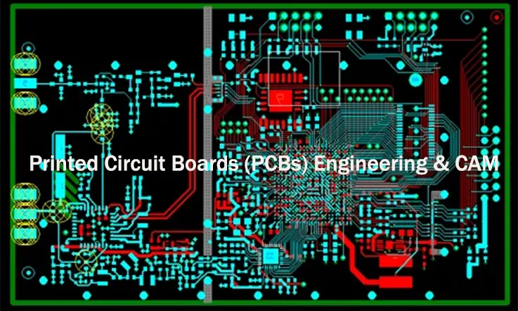
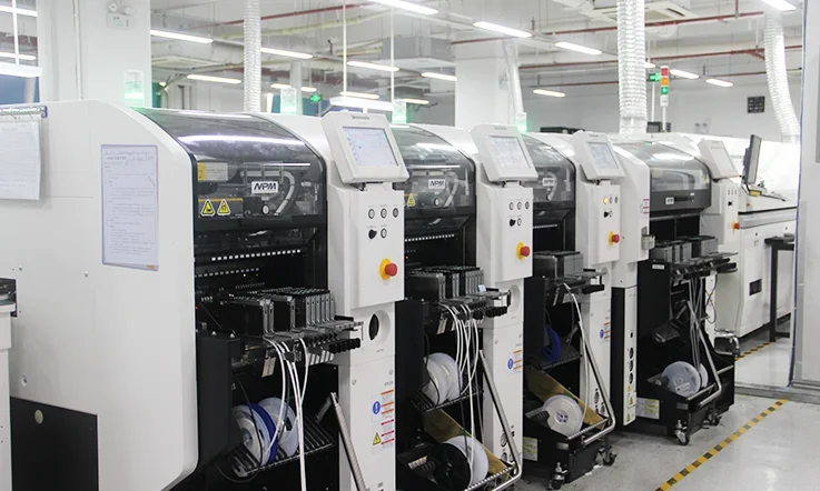
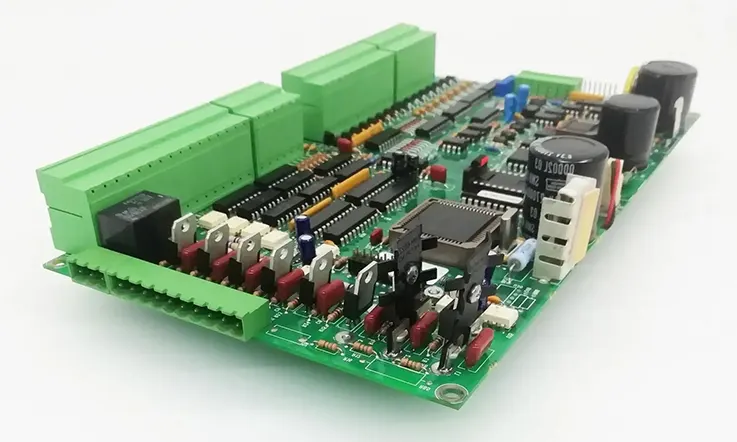
Printed Circuit Board (PCB) engineering and Computer-Aided Manufacturing (CAM) are like the bread and butter of modern electronics production. Every gadget, from smartphones to aerospace control systems, depends on PCBs that are precisely designed and flawlessly manufactured. But here’s the catch—getting a PCB from design to reality isn’t just about placing components on a board. The process demands a seamless transition between PCB engineering and PCB CAM to avoid costly errors, manufacturing delays, and functional mishaps.
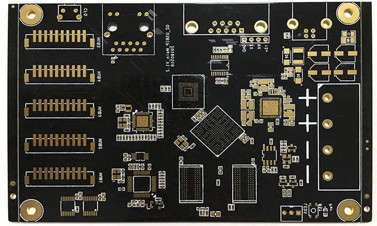
In addition, as electronic devices become more advanced, PCB engineering faces increasing demands in signal integrity, power efficiency, thermal management, and miniaturization. From high-density interconnect (HDI) PCBs to multi-layer stack-ups, modern designs require precise layout techniques, optimized routing, and manufacturable structures. This is where PCB CAM (Computer-Aided Manufacturing) software steps in, bridging the gap between ECAD design and fabrication processes.
In this guide, we’re diving deep into how PCBs engineering and PCB CAM work together, breaking down industry best practices, advanced techniques, and how the right software tools can save you from pulling your hair out.
Introduction to PCBs Engineering and PCB CAM
Designing and manufacturing printed circuit boards isn’t just about connecting components and sending them off to production. Every choice in PCB layout, material selection, trace routing, and stack-up configuration affects the performance, reliability, and cost of the final product. But even the most carefully designed board can run into issues if it isn’t optimized for fabrication and assembly.
That’s where PCB CAM (Computer-Aided Manufacturing) steps in. By refining Gerber file processing, CAM tooling adjustments, and DFM/DFT/DFA analysis, PCB CAM ensures that a design is ready for production without last-minute surprises.
This section dives into PCB engineering fundamentals, the role of PCB CAM in manufacturing, and how automation is reshaping the industry. Engineers refining a design and manufacturers aiming to reduce errors must understand these processes to achieve the best results.
What is PCBs Engineering?
The world of PCB engineering revolves around more than just drawing circuit connections. Every PCB must be designed with electrical performance, manufacturability, and long-term reliability in mind. A board that looks great on-screen might be a nightmare to produce if it ignores real-world constraints.
Core Aspects of PCB Engineering-
A well-planned PCB starts with a solid understanding of these elements:
●PCB Layout – Arranging traces, vias, and components in a way that supports signal integrity and power distribution.
●PCB Stack-Up – Choosing the right number and arrangement of layers to balance performance and cost.
●Trace Routing – Determining the best way to connect components while reducing interference.
●High-Speed PCB Design – Managing signal integrity for fast data transmission in applications like RF, DDR, and PCIe circuits.
●Fabrication Process – Understanding how different materials, etching methods, and via structures affect the manufacturability of the PCB.
Industry Applications of PCBs Engineering-
Different sectors require unique PCB engineering approaches:
●Automotive Electronics – Modern vehicles use multi-layer PCBs for safety, infotainment, and power management.
●Consumer Devices – Smartphones, laptops, and smart home products demand high-density, lightweight PCB designs.
●Medical Equipment – Life-saving devices depend on strict signal integrity and low electromagnetic interference (EMI).
Note: If you’re designing PCBs, ignoring real-world constraints is a shortcut to failure. Material selection, signal integrity, and manufacturing limitations all play a huge role in getting a product to market successfully.
Understanding PCB CAM and Its Role in Manufacturing Optimization
Once a PCB design is finalized, it needs to be translated into machine-readable instructions for fabrication, assembly, and testing. This is where PCB CAM software becomes a necessity. It bridges the gap between design and production, ensuring that everything aligns with factory capabilities.
How PCB CAM Converts a Design into a Manufacturable Product-
PCB CAM tools take the original design files and apply a series of automated checks and adjustments to prepare them for production. This process includes:
●Gerber File Processing – Converting PCB layouts into a format that fabrication machines can read.
●DFM (Design for Manufacturing) Checks – Identifying clearance issues, minimum trace widths, and material limitations.
●DFA (Design for Assembly) Validation – Ensuring that components are positioned for automated assembly without defects.
●DFT (Design for Testability) Enhancements – Adding test points and features that make post-production verification easier.
●CAM Tooling Adjustments – Fine-tuning solder mask layers, silkscreens, and panel layouts for efficiency.
Skipping PCB CAM processing can lead to unforeseen fabrication errors, component misalignment, and wasted material—all of which translate to higher costs and delays.
The Impact of CAM Optimization on Manufacturing Efficiency-
Well-optimized CAM files allow manufacturers to:
●Reduce scrap rates by eliminating design-related issues before fabrication. ●Improve yield by ensuring panelization layouts maximize material usage. ●Speed up production by minimizing last-minute engineering revisions.
Investing time in DFM/DFA/DFT analysis during the PCB CAM stage prevents costly surprises later. Catching problems early means fewer delays, lower costs, and a more predictable production timeline.
The Evolution of PCB CAM and Modern Trends in PCB Engineering
Gone are the days when PCB CAM involved manual file adjustments and trial-and-error corrections. Today, automation and AI-driven analysis have reshaped how designs are prepared for manufacturing.
Advancements in Automated PCB CAM Processing-
Modern PCB CAM software has taken a huge leap forward with AI-assisted verification, predictive analysis, and real-time design adjustments. Instead of we manually reviewing every layer and trace, machine learning algorithms now detect potential production bottlenecks before they happen.
This automation speeds up the process while reducing human errors, making it possible to optimize stack-up designs, drill hole placements, and solder mask definitions with minimal manual intervention.
Cloud-Based PCB CAM and Collaborative Manufacturing-
With more design and manufacturing teams spread across different locations, cloud-based PCB CAM tools allow engineers, PCB fabricators, and assemblers to collaborate in real time. This eliminates the need for constant file exchanges and version mismatches, streamlining the entire workflow.
We can flag a trace width issue or silkscreen misalignment, and our designer can fix it instantly—no back-and-forth emails required. This kind of real-time collaboration minimizes revision cycles and keeps production on schedule.
AI-Driven PCB Engineering and Smart Manufacturing-
Artificial intelligence isn’t just making PCB CAM faster—it’s making it smarter. AI-powered tools can:
●Predict signal integrity issues before prototyping.
●Optimize trace routing for lower EMI and better thermal management.
●Suggest panelization layouts that improve material efficiency.
Essential PCB CAM Processes in PCBs Engineering
The journey from a PCB design concept to a fully fabricated board isn’t just about drawing traces and dropping components on a layout. Without proper CAM processing, even the best designs can run into manufacturing roadblocks, leading to production setbacks and unnecessary costs.
This is why PCB CAM processes play a huge role in bridging the gap between design and fabrication. CAM software ensures that every design is not just functional on screen but also manufacturable on the factory floor.
From preparing design files to optimizing layouts for fabrication and automating error detection, let’s dive into what makes PCB CAM a must-have in modern electronics manufacturing.
Preparing PCB Design Files for CAM Processing
Before a PCB design can move to fabrication, it needs to be translated into a format that PCB manufacturers can understand. PCB CAM software acts as the interpreter, converting complex designs into precise fabrication instructions.
Choosing the Right File Format for Manufacturing-
PCB designs are typically handed off in a few standard file formats, each catering to specific fabrication needs.
Consolidates fabrication, assembly, and testing data
Comprehensive, reduces file misinterpretation
IPC-2581
Vendor-independent format for design-to-fabrication integration
Standardized for modern PCB production
Netlist Files
Ensures circuit connectivity correctness
Prevents fabrication mismatches
●Gerber Files (RS-274X) – The industry standard for defining PCB layers, including copper, solder mask, and silkscreen layers.
●ODB++ – A comprehensive format that consolidates fabrication, assembly, and testing data into a single package.
●IPC-2581 – A neutral, vendor-independent format designed for seamless integration across different manufacturing environments.
●Netlist Files – Ensures that the fabricated PCB matches the original circuit connections.
Sending incomplete or improperly formatted files to a circuit boards manufacturer can cause delays, misinterpretations, or even faulty production runs. That’s why CAM engineers run verification checks before fabrication begins.
Netlist Verification: Catching Hidden Errors Before Production-
A PCB layout might look fine, but unseen errors can cause massive headaches if they aren’t caught early. Netlist verification compares the PCB layout against the original circuit design to ensure:
●No missing connections that could cause open circuits.
●No unintended shorts between traces or components.
●Proper alignment of copper layers to prevent mismatches in multilayer PCBs.
Potential Issue
Impact on PCB
Missing connections
Causes open circuits, rendering PCB non-functional
Unintended shorts
Leads to electrical failures and component damage
Misaligned copper layers
Creates mismatches in multilayer PCBs
Skipping this step could mean discovering issues only after production, turning what should have been a seamless build into an expensive rework job.
Panelization Techniques: Making Manufacturing Efficient-
Once the PCB design is validated, the next step is panelization—the process of arranging multiple PCB units onto a single panel for fabrication. Proper panelization ensures:
●Efficient use of materials, reducing waste and lowering costs.
●Easier handling during assembly, minimizing production errors.
●Simplified depaneling, preventing mechanical stress on individual boards.
Panelization Benefit
Outcome
Efficient material usage
Reduces waste and lowers costs
Easier handling during assembly
Minimizes production errors
Simplified depaneling
Prevents mechanical stress on individual boards
Ignoring panelization best practices could lead to warped PCBs, alignment issues, and excessive material waste.
Heads-up: Not all manufacturers support every file format, so always check fabrication guidelines before sending your design files.
How PCB CAM Optimizes Design for Manufacturability?
Even if a PCB is perfectly designed, it doesn’t always mean it’s easy to manufacture. PCB CAM software ensures that designs are not just electrically sound but also optimized for fabrication and assembly.
DFM Checks: Preventing Costly Production Mistakes-
Addressing these issues upfront reduces scrap rates, prevents delays, and saves money on production runs.
DFA Considerations: Ensuring a Smooth Assembly Process-
Even if a PCB is perfectly fabricated, poor assembly planning can turn production into a nightmare. CAM software runs DFA (Design for Assembly) checks to make sure:
●Components are properly spaced to accommodate automated pick-and-place machines.
●Silkscreen labels are readable after assembly, avoiding confusion during manual inspections.
●Solder pad sizes are optimized for proper wetting, reducing the risk of cold joints.
DFA Check
Reason
Component spacing
Allows room for automated pick-and-place machines
Silkscreen readability
Prevents confusion during manual inspections
Solder pad size optimization
Ensures proper wetting, reducing cold joints
If these issues aren’t caught early, they could lead to assembly defects, increased labor costs, and unnecessary rework.
PCB CAM Automation: Reducing Errors and Enhancing Production Yield
Gone are the days of manual CAM reviews—today’s many PCB fabrication houses use advanced automation tools to detect errors and fine-tune designs for better production results.
How Automated DFM Tools Improve Manufacturing Readiness-
Modern CAM software applies automated DFM rule sets to detect common issues instantly. These automated checks help with:
●Ensuring via drill sizes are within PCB manufacturer tolerances.
●Detecting silkscreen overlaps that could cause confusion in assembly.
●Balancing copper distribution to prevent PCB warping.
Automated Check
Key Improvement
Via drill size verification
Ensures manufacturability
Silkscreen overlap detection
Prevents component misidentification
Copper balancing
Reduces PCB warping
By automating these checks, we can reduce human error, improve fabrication accuracy, and accelerate production timelines.
The Role of CAM Rule Sets in Maintaining Quality-
PCB fabs develop custom CAM rule sets tailored to their equipment and processes. These rules ensure:
●Minimum trace widths and spacings are met for a given etching process.
●Drill hole tolerances align with plating and routing capabilities.
Failing to adhere to these guidelines can lead to fabrication defects, costly rework, and yield loss.
Boosting Production Yield Through Smart CAM Adjustments-
Every PCB manufacturer aims to maximize yield—getting the highest number of fully functional boards from a production batch. PCB CAM tools help improve yield by:
●Refining solder mask clearances to prevent unintended shorts.
●Optimizing stencil designs to ensure consistent solder paste application.
●Adjusting copper balancing to reduce thermal and mechanical stress.
Optimization
Yield Improvement
Refining solder mask clearances
Prevents unintended shorts
Optimizing stencil designs
Ensures consistent solder paste application
Adjusting copper balancing
Reduces thermal and mechanical stress
By integrating these automated processes, PCB CAM significantly enhances production efficiency while maintaining high-quality standards.
Advanced PCB Stack-Up Design and Signal Integrity in PCBs Engineering
In PCB design, setting up the right stack-up configuration, maintaining signal quality, and managing heat effectively help achieve reliable performance. For designs like multi-layer boards and high-speed circuits, these aspects require even more attention, as each layer and its interactions affect overall functionality. We must carefully plan each layer’s design to prevent potential performance issues.
This section will focus on the specific processes and considerations in PCB CAM that help achieve optimal signal integrity and thermal performance, reducing potential design flaws and maximizing the operational efficiency of the final PCB product.
PCB CAM Considerations for Multi-Layer and High-Speed PCB Stack-Ups
Multi-layer PCBs are essential when dealing with complex designs and high-density circuits, but they bring about challenges in signal transmission and thermal management. In these designs, PCB CAM tools assist by validating factors like impedance control, trace width, and material selection.
Controlled Impedance and Dielectric Materials-
In high-speed circuits, maintaining controlled impedance is essential to prevent signal degradation. PCB CAM tools ensure that traces are routed according to impedance rules that help maintain signal quality, particularly in high-frequency designs.
●Dielectric materials influence signal propagation velocity. PCB CAM software can analyze design requirements and recommend suitable materials, assisting our engineers in selecting the most appropriate option for each application.
●Trace width and spacing affect impedance consistency. By verifying that traces adhere to specified width parameters, PCB CAM tools support precise signal transmission and minimize signal reflection.
Trace Width Calculations and Multi-Layer Routing-
Correct trace width is more than just fitting within the available space—it’s about ensuring that signals can travel without causing interference.
●PCB CAM tools allow engineers to run simulations for trace width to ensure that each design specification is met. This includes the careful routing of traces across multiple layers to avoid noise and interference between signal paths.
●Multi-layer routing in high-speed designs requires precision in terms of both trace width and layer allocation, preventing cross-talk and signal coupling.
Proper planning and use of PCB CAM software streamline the routing process, ensuring minimal distortion across the design.
Power and Ground Layer Optimization-
Power and ground planes help maintain voltage stability and reduce electromagnetic interference (EMI). PCB CAM tools provide:
●Ground plane optimization to ensure continuous coverage, which helps reduce signal noise and improves signal quality.
●Power plane design to maintain stable voltage levels across the board.
Correctly designed power and ground layers help in reducing noise and ensuring that the power distribution network (PDN) operates effectively throughout the design.
Signal Integrity and Power Integrity Optimization Through PCB CAM
Signal integrity and power integrity are major considerations for high-speed designs, ensuring that signals travel through the PCB without degradation and power is delivered efficiently to the components.
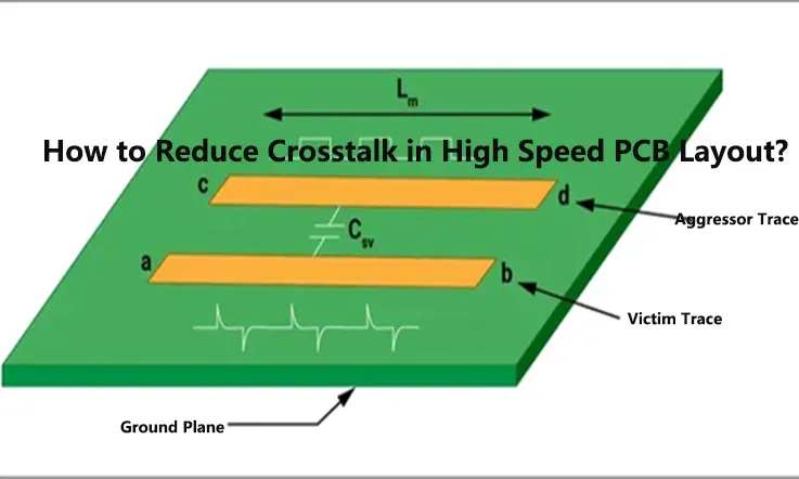
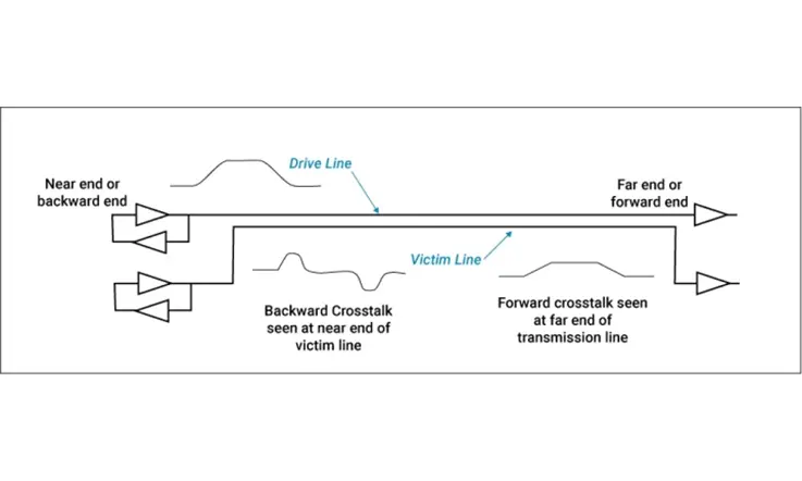
Minimizing EMI and Crosstalk-
Electromagnetic interference (EMI) can lead to signal distortion and operational instability in high-speed PCBs. PCB CAM tools address this by:
●Ensuring proper trace separation to minimize crosstalk between traces, especially when dealing with sensitive signals.
●Optimizing return paths and integrating shielding around sensitive areas to protect against external EMI.
These optimizations are automated in PCB CAM tools, ensuring that designs meet stringent EMI regulations while minimizing potential interference.
Differential Pair Routing and Layout Optimization-
For high-speed differential signals, proper routing is necessary to ensure signals arrive in sync at the receiving end. PCB CAM software automates the routing of differential pairs, ensuring that:
●The traces are matched in length for synchronized signal transmission.
●The spacing between differential pairs is consistent, helping minimize potential noise or signal degradation.
Optimized differential pair routing helps maintain signal fidelity for high-speed applications, such as data transfer in high-performance computing and communication systems.
Power Delivery Optimization-
Ensuring stable and uniform power delivery to components is a challenge in complex PCB designs. Through PCB CAM, we can:
●Simulate IR drop to check for voltage fluctuations across the PCB, ensuring that power integrity is maintained.
●Perform current density analysis to avoid overheating or inefficient power delivery to components.
Efficient power delivery improves overall device performance, preventing component failures due to power inconsistencies.
Thermal Management and PCB CAM Strategies for Heat Dissipation
Managing heat in high-density PCBs is necessary, especially for high-power circuits. Without proper dissipation, excessive heat may cause component damage or reduced performance.
Thermal Vias and Copper Pours for Heat Dissipation-
Thermal vias are an effective solution to help conduct heat away from high-power components. PCB CAM tools help:
●Optimize via placement for maximum heat transfer from sensitive areas.
●Design copper pours for effective thermal distribution across the PCB.
Thermal management is achieved by ensuring heat flows efficiently from the components to the outer layers of the PCB where it can be dissipated.
Using Heat Sinks and Passive Cooling-
For components that generate significant heat, additional measures like heat sinks and thermal pads are employed. PCB CAM can assist in:
●Planning the integration of heat sinks and thermal vias to promote better heat dissipation.
●Ensuring that materials used for heat sinks are compatible with the PCB design for optimal performance.
Heat dissipation is a main factor in ensuring that components remain within operating temperatures.
Material Selection for Thermal Performance-
Choosing the right materials for a PCB impacts not just electrical performance but also thermal dissipation. PCB CAM tools can help us choose materials with higher thermal conductivity, making it easier to dissipate heat and maintain performance in thermal-heavy applications.
Ensuring PCB Quality Control Through PCB CAM Analysis
Every stage of PCB manufacturing comes with potential issues that can impact the final product. Defects not only lead to scrap and wasted resources but can also result in electrical failures and unreliable performance in end-use applications. This is where PCB CAM (Computer-Aided Manufacturing) steps in as a gatekeeper, catching design flaws before they escalate into costly production errors.
More than just a verification tool, PCB CAM acts as an early-warning system that detects issues in design files, optimizes layout for manufacturing, and minimizes errors during fabrication and assembly. The following sections will explore how PCB CAM enhances production efficiency, reduces defect rates, and ensures electrical performance through rigorous testing.
How PCB CAM Enhances Manufacturing Yield and Reduces Defects?
To maintain stable PCB production, minimizing defects is a top priority. Leveraging PCB CAM allows manufacturers to simulate production conditions, spot potential failures, and make corrections before fabrication even begins.
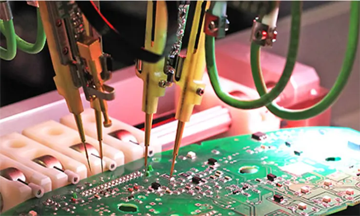
Automated Optical Inspection (AOI) and X-ray Inspection-
Throughout production, AOI (Automated Optical Inspection) quickly identifies missing components, poor solder joints, short circuits, and open traces. Using high-resolution cameras, AOI scans the PCB surface far more efficiently than manual inspection, significantly reducing human error.
For hidden solder joints, such as Ball Grid Array (BGA) components, X-ray inspection becomes essential. It reveals hidden defects like voids, cold solder joints, and misalignments. Integrating AOI and X-ray inspection within PCB CAM creates a closed-loop system where design and production teams can make real-time adjustments to improve overall manufacturing quality.
Solder joint reliability directly impacts PCB longevity. If reflow soldering temperatures are not properly controlled, issues such as cold solder joints, bridging, or incomplete wetting can occur. PCB CAM simulates solder joint behavior and optimizes the reflow temperature curve to ensure proper bonding.
Additionally, PCB CAM evaluates pad design, ensuring that pad sizes match component leads, eliminating pad misalignment issues, and preventing problems like tombstoning or solder paste misplacement.
Panel Optimization to Improve Material Utilization-
For high-volume production, panel layout significantly affects manufacturing costs. Poor panel design wastes substrate material and can lead to mechanical stress issues. PCB CAM applies panelization algorithms to determine the most efficient layout, maximizing the number of PCBs per panel while preventing mechanical failures like board warping or cracking.
Design Rule Check (DRC) in PCB CAM: Preventing Common PCB Errors
Many PCB failures originate from design errors, including inadequate trace widths, via violations, and misaligned solder masks. If these mistakes go unnoticed in the design phase, they can lead to performance degradation, electrical shorts, or manufacturability issues. PCB CAM performs DRC (Design Rule Check) to automatically detect these violations before the design moves to production, saving time and preventing costly rework.
Via and Annular Ring Clearance Checks-
Vias connect different PCB layers, but if poorly designed, they can cause electrical and soldering issues. PCB CAM verifies via size, annular ring clearance, and pad-to-via spacing to ensure robust electrical connections and reliable manufacturing.
Design Parameter
Optimal Value Range
Potential Issue if Violated
Via Diameter
0.2mm – 0.5mm
Weak electrical connections
Annular Ring Width
≥ 0.1mm
Poor plating adhesion, open circuits
Pad-to-Via Clearance
≥ 0.2mm
Risk of solder bridging, short circuits
Trace Width, Spacing, and Drill Hole Tolerance Control-
Every PCB trace must adhere to minimum width and spacing guidelines to prevent short circuits and impedance mismatches. PCB CAM measures signal traces, calculates impedance matching, and detects violations to ensure compliance with fabrication tolerances.
Drill hole tolerances also require strict control. If via holes deviate from specified dimensions, they may cause plating failures or lead to mechanical instability. PCB CAM automatically checks drill hole sizes to ensure they remain within acceptable limits.
Solder Mask Alignment Verification-
The solder mask protects PCB surfaces from oxidation and accidental solder bridging. However, if misaligned, exposed copper can create short circuits or lead to corrosion. PCB CAM runs precise solder mask alignment checks, correcting misalignments to maintain circuit reliability over time.
Implementing Electrical Testing (DFT) with PCB CAM for Reliability
Even after a PCB is built according to specifications, verifying its electrical functionality remains necessary. DFT (Design for Testability) ensures each PCB undergoes comprehensive electrical testing before use. PCB CAM helps plan and refine test points, making testing more straightforward and enhancing reliability.
Flying Probe Testing and In-Circuit Testing (ICT)-
Flying Probe Testing is ideal for prototype and low-volume production since it provides flexible, point-by-point electrical testing without requiring a custom fixture. PCB CAM optimizes probe paths to minimize test time while maximizing fault detection.
For high-volume production, In-Circuit Testing (ICT) is the preferred approach. ICT relies on Bed-of-Nails test fixtures, allowing simultaneous testing of multiple circuits. PCB CAM ensures that test points are optimally placed, preventing the risk of untestable connections that could cause functional failures later on.
Test Method
Best for
Key Advantage
Limitations
Flying Probe Testing
Low-volume, prototyping
No fixture required, flexible
Slower than ICT
In-Circuit Testing (ICT)
High-volume production
Fast, parallel testing
Requires custom fixture
Functional Testing and Test Point Optimization-
Beyond basic continuity checks, functional testing examines real-world circuit behavior, such as signal integrity, power consumption, and thermal performance. PCB CAM arranges test point distribution to guarantee access to all essential nodes, allowing functional tests to cover all necessary electrical paths.
How Choosing PCB CAM Software for Efficient PCB Engineering?
Printed circuit board production relies on precise data handling, thorough design verification, and seamless integration between design and fabrication. PCB CAM software acts as the bridge between electronic design automation (EDA) tools and the manufacturing floor, ensuring that layouts are checked for manufacturability, fabrication data is properly formatted, and potential issues are caught before production.
With multiple options available, selecting the right PCB CAM tool depends on its capabilities, compatibility with design software, and how well it supports automated checks and optimization. Understanding how these tools function can help avoid common errors, streamline production, and improve overall workflow efficiency.
Comparing PCB CAM Software: Features and Performance
Different PCB CAM solutions cater to various stages of the fabrication process. Some focus on validating designs, while others provide in-depth panelization and automated manufacturing checks. Below are some widely used options:
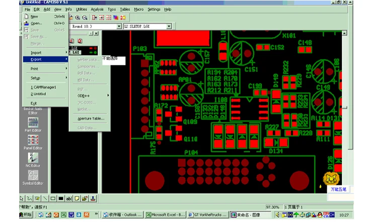
1. CAM350-
A widely used solution that allows engineers to inspect, edit, and verify PCB designs before manufacturing. It includes design rule checks (DRC), panelization tools, and Gerber file editing, making it a preferred choice for preparing boards for fabrication.
2. Altium CAM Editor-
Built into Altium Designer, this tool simplifies the transition from ECAD to CAM by offering native support for Gerber, ODB++, and IPC-2581 formats. It is particularly useful for those already working in the Altium environment.
3. Valor NPI-
Developed by Siemens, this software specializes in automated design-for-manufacturability (DFM) analysis, identifying potential assembly challenges like incorrect component footprints, solder paste misalignment, and electrical testability issues.
4. Genesis and Frontline InCAM-
Both developed by Orbotech (now part of KLA Corporation), these tools are widely adopted by PCB manufacturers. Genesis offers extensive CAM editing and fabrication job preparation, while Frontline InCAM enhances process automation, panel optimization, and manufacturability improvements.
5. Ucamco Integr8tor-
This software is designed to automate PCB data analysis and generate instant manufacturability reports. It is particularly useful for fabricators who need to assess multiple designs quickly without extensive manual input.
Each tool offers a different balance of features, and the right choice depends on project requirements, manufacturing complexity, and how well it integrates into existing workflows.
What to Look for When Choosing PCB CAM Software?
Selecting PCB CAM tools involves considering several factors that impact design verification, fabrication readiness, and overall efficiency. Some of the core areas to evaluate include:
1. Error Detection and Design Verification-
Fabrication defects often stem from design oversights such as trace width violations, solder mask misalignment, and annular ring clearance issues. A robust PCB CAM tool should automatically flag these concerns, preventing costly rework.
2. Integration with ECAD Tools-
For teams using design software like Altium, Cadence, or KiCad, seamless data transfer to CAM software is necessary. Direct compatibility minimizes conversion errors and speeds up manufacturing preparation.
3. Automation and Workflow Optimization-
Modern PCB CAM tools include automation features such as DFM checks, panelization, and test point optimization. These functions reduce manual intervention and accelerate the transition from design to production.
4. File Format Support-
A well-rounded PCB CAM system should support widely used fabrication formats, such as:
●Gerber (RS-274X) – The standard format for PCB manufacturing
●ODB++ – A richer format preferred for seamless data exchange
●IPC-2581 – A modern open-standard format improving industry-wide compatibility
5. Vendor Support and Software Updates-
Manufacturing processes evolve, and having access to software updates and technical support ensures that engineers can keep up with new fabrication requirements and technological advancements.
Integrating PCB CAM Software into PCB Design and Fabrication
Smooth integration between design tools and CAM software eliminates manual errors and speeds up production. The following workflow outlines how PCB CAM tools fit into the overall PCB fabrication process:
1. ECAD to CAM Transition-
After finalizing a PCB layout, the design is exported in a manufacturing-ready format (e.g., Gerber, ODB++, IPC-2581). The CAM software then runs validation checks to ensure the design meets fabrication guidelines.
2. Automated DFM Analysis-
Advanced PCB CAM tools provide real-time feedback, enabling we to resolve manufacturability issues before production begins. This minimizes fabrication delays and avoids unnecessary re-spins.
3. Manufacturing File Preparation-
Once the CAM review is complete, the software generates essential files for production, including:
●NC Drill files for defining hole placements
●Solder paste layers for stencil creation
●Panel layouts to optimize material usage
4. Smart Factory and Process Automation-
Some advanced PCB CAM solutions integrate with smart manufacturing systems, enabling real-time monitoring, predictive analysis, and adaptive process adjustments. This helps improve fabrication efficiency and consistency.
PCB CAM Tooling and Manufacturing Guidelines in PCB Engineering
Manufacturing a PCB requires more than just following a blueprint. Every step, from panelization to solder mask application and material utilization, must be carefully managed to avoid unnecessary costs and production delays. PCB CAM tooling plays a direct role in shaping fabrication efficiency, ensuring smooth transitions between design, assembly, and testing.
A carefully planned CAM processing approach helps eliminate design bottlenecks, reduce material waste, and maintain efficient production timelines. Below are some of the most effective strategies utilized in PCB CAM tooling and manufacturing.
Understanding PCB Panelization and Tooling Optimization in CAM
Panelization allows multiple PCBs to be produced together, making fabrication faster and reducing handling time. The way boards are arranged in a panel affects everything from material usage to assembly precision.
1. Breakaway Tabs and V-Scoring: Choosing the Right Separation Method-
When manufacturing in bulk, individual PCBs need a clean and efficient separation method. Two common techniques are:
●Breakaway Tabs: These small sections of material hold the PCB in place during fabrication. To make them easier to remove, they often feature perforations, sometimes referred to as “mouse bites.”
●V-Scoring: A shallow cut is made along the surface of the PCB, allowing it to snap apart after assembly. This method works well for straight-edged designs and high-volume runs.
Separation Method
Advantages
Disadvantages
Breakaway Tabs
Easy to implement, supports irregular shapes
May leave rough edges, requires more space
V-Scoring
Ideal for straight edges, fast removal
Not suitable for complex board shapes
2. Routing vs. Punching for PCB Separation-
The method used to detach boards from a panel affects speed and material usage.
●Routing: A CNC machine mills out the board shape. This method is flexible but generates more waste.
●Punching: A dedicated press quickly separates PCBs using a pre-made die. This approach is faster but requires upfront tooling investment.
3. Fiducial Marks for Precise SMT Pick-and-Place Alignment-
Fiducial marks act as reference points for automated assembly equipment. Without them, pick-and-place machines may misalign components, especially on dense PCBs. To improve accuracy, these small copper pads should be:
●Placed symmetrically on opposite corners of the board.
●Free from solder mask or silkscreen coverage.
●Consistently sized across all production runs.
4. Panel Layout and Waste Reduction-
Maximizing panel efficiency lowers material costs. By arranging PCBs tightly without unnecessary gaps, we minimize wasted substrate and improve overall yield. Strategic nesting of boards allows for better material utilization.
Solder Mask, Silkscreen, and Copper Layer Considerations in PCB CAM
Fine-tuning solder mask openings, silkscreen placement, and copper balancing prevents defects and enhances durability. These layers do more than just protect the PCB—they influence long-term performance.
1. Solder Mask Openings and PCB Protection-
The solder mask prevents unintended solder bridges, oxidation, and contamination. However, certain areas must remain exposed for proper assembly:
●Component pads must be fully open to allow solder adhesion.
●Clearance between mask openings and copper traces must be carefully set to avoid exposure issues.
●For fine-pitch components, a properly defined mask prevents shorts and alignment errors.
Solder Mask Design Factor
Impact on PCB Manufacturing
Potential Issue if Ignored
Pad Opening Size
Ensures solderability without bridging
Cold joints or solder shorts
Clearance from Traces
Prevents unintended copper exposure
Electrical shorts
Fine-Pitch Mask Definition
Supports precise component placement
Misalignment and solder issues
2. Silkscreen Readability and Placement-
Silkscreen markings provide component labels, polarity indicators, and assembly guidance. To avoid issues during production:
●Text should be large enough to remain readable after printing.
●Avoid placing silkscreen on solder pads, which can interfere with soldering.
●Use high-contrast colors for better legibility (e.g., white silkscreen on a green mask).
3. Copper Layer Balancing to Prevent PCB Warping-
Uneven copper distribution leads to mechanical stress during thermal cycling. To avoid board warping and twisting, copper layers must be evenly distributed. Techniques include:
●Adding copper fills in low-density areas to even out material distribution.
●Symmetrically designing inner and outer copper layers to avoid stress imbalances.
4. Surface Finish Selection: HASL, ENIG, and OSP-
The type of surface finish affects solderability, oxidation resistance, and long-term reliability. Common choices include:
●HASL (Hot Air Solder Leveling): Economical but not ideal for fine-pitch components.
●OSP (Organic Solderability Preservative): A cost-effective, lead-free option with a shorter shelf life.
Choosing the right finish depends on assembly requirements, environmental exposure, and storage conditions.
Cost Optimization Strategies in PCB CAM for Large-Scale Manufacturing
Efficient CAM strategies help us reduce material usage, minimize processing time, and eliminate unnecessary expenses. These approaches streamline production while maintaining quality.
1. Maximizing Material Utilization-
The more efficiently a panel is arranged, the less material is wasted. Manufacturers optimize layouts by:
●Minimizing gaps between PCBs to fit as many boards as possible per panel.
●Standardizing board sizes to simplify production planning.
●Using shared tooling strips to reduce cutting waste.
Optimization Strategy
Material Savings
Impact on Cost
Tight PCB Nesting
Reduces unused panel space
Lower material costs
Standardized PCB Dimensions
Simplifies panel arrangement
Faster production setup
Shared Tooling Strips
Minimizes cutting waste
Less scrap and higher yield
2. Reducing Drill Costs by Limiting Hole Variations-
Drilling is one of the slowest steps in PCB fabrication. The fewer drill bit changes required, the faster the process. Cost-saving techniques include:
●Standardizing via and hole sizes instead of using many different diameters.
●Avoiding microvias unless necessary, as they require advanced drilling techniques.
3. Cutting Production Waste by Catching Errors Early-
CAM software catches many common design mistakes before fabrication begins, such as:
●Missing solder mask clearances
●Overlapping silkscreen on pads
●Incorrect drill-to-pad alignment
Addressing these errors ahead of time prevents costly rework and material loss.
4. Faster Turnaround with Automated CAM Processing-
Modern CAM software automates design verification, panelization, and manufacturing prep, reducing the time from design submission to production. This speeds up delivery schedules and increases overall efficiency.
5. Large-Scale Batch Processing Efficiency-
For high-volume manufacturing, batch processing saves both time and money. Strategies include:
●Combining multiple small orders into a single production run.
●Pre-optimizing solder mask and paste layers for repeatable consistency.
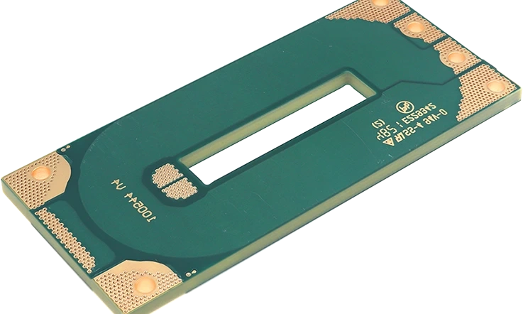
High-Density Interconnect (HDI) PCBs and PCB CAM Challenges
As electronic devices become more compact and complex, HDI (High-Density Interconnect) PCBs have become a best choose solution for maximizing functionality within limited space. These circuit boards rely on microvias, fine-pitch components, and multi-layer stack-ups, pushing fabrication techniques to their limits.
Unlike standard PCBs, HDI designs demand precision at every stage, from via formation to layer registration. Without CAM-driven verification, manufacturers risk misalignment, material waste, and inconsistent electrical performance.
Let’s explore how PCB CAM ensures smooth HDI fabrication, covering design preparation, manufacturing accuracy, and cost-efficient strategies.
Why HDI PCBs Require Advanced PCB CAM Techniques?
HDI designs challenge traditional fabrication methods, requiring laser-drilled vias, sequential lamination, and controlled layer stack-ups. Proper CAM processing prevents costly mistakes that could disrupt production.
1. Microvia Design and Via-in-Pad Implementation-
Unlike mechanically drilled vias, microvias are laser-drilled and must be carefully positioned to maintain electrical performance and structural reliability. PCB CAM plays a role in:
●Ensuring microvia alignment across multiple layers.
●Checking aspect ratio limitations to prevent reliability issues.
●Optimizing via-in-pad structures to support high-speed signals without unwanted electrical interference.
2. Sequential Lamination and HDI Layer Stack-Up-
HDI PCBs rely on sequential lamination, where multiple fabrication steps increase the chance of misalignment, resin starvation, and warping. PCB CAM reduces these risks by:
●Simulating layer compression effects before production.
●Verifying drill-to-copper spacing to maintain electrical clearance.
●Automating impedance calculations to meet signal integrity requirements.
3. Fine-Pitch Component Placement and Routing Adjustments-
With BGA (Ball Grid Array) and CSP (Chip Scale Package) components shrinking to 0.4mm pitch and below, routing traces between pads requires careful planning. PCB CAM enhances this process by:
●Applying automated fan-out routing to escape dense pin grids.
●Adjusting trace width-to-space ratios based on fabrication tolerances.
●Generating high-resolution manufacturing plots to prevent etching defects.
Overcoming Manufacturing Challenges of HDI PCBs with PCB CAM
HDI fabrication introduces challenges that extend beyond standard PCB manufacturing, from laser drilling precision to impedance-controlled routing. Addressing these factors through CAM-driven analysis and verification leads to more consistent results.
1. Laser Drilling Accuracy for Microvias-
HDI PCBs require laser-drilled microvias that must align precisely with inner copper layers. PCB CAM enhances accuracy by:
●Generating optimized drill coordinates to prevent breakouts.
●Applying correct laser ablation settings to avoid over-etching.
●Verifying stacking rules to avoid structural weaknesses.
2. Via-in-Pad Technology and Planarization Considerations-
Via-in-pad structures improve signal transmission but require planarization techniques to avoid assembly defects such as solder voids and uneven surfaces. PCB CAM helps by:
●Defining appropriate solder mask clearances to prevent solder wicking.
●Recommending resin fill or copper cap methods for a smooth finish.
●Simulating thermal expansion effects to prevent layer delamination.
3. High-Aspect Ratio Vias and Plating Control-
High-aspect ratio vias (depth-to-diameter ratio >10:1) require precise plating techniques to ensure electrical continuity without mechanical stress. CAM-driven plating analysis assists by:
●Calculating copper thickness requirements for consistent conductivity.
●Optimizing drill parameters to prevent hole breakage.
●Predicting plating uniformity issues before fabrication starts.
4. Impedance-Controlled Routing and Signal Integrity Preservation-
HDI PCBs carry high-speed signals, making impedance consistency a priority. CAM software assists by:
●Adjusting trace width and spacing based on dielectric constants.
●Adding controlled impedance test structures for validation.
●Preventing signal degradation through automated checks.
5. Registration Precision for Layer-to-Layer Alignment-
As HDI stack-ups grow in complexity, misalignment between layers can result in shorts, open circuits, or fabrication scrap. PCB CAM reduces these risks by:
●Providing fiducial alignment analysis for precise layer registration.
●Simulating shrinkage and expansion effects during lamination.
●Applying dynamic adjustments to compensate for potential material distortion.
PCB CAM Strategies for Reducing Cost and Complexity in HDI PCB Production
HDI PCBs increase fabrication expenses due to specialized materials, advanced drilling techniques, and additional process steps. CAM-driven solutions help optimize manufacturing efficiency while maintaining product performance.
1. Optimizing Panel Utilization to Reduce Material Waste-
HDI PCBs often require custom panel layouts, but inefficient planning leads to higher material waste. CAM software assists in:
●Nestling smaller boards together to improve material efficiency.
●Minimizing border clearances while maintaining fabrication tolerances.
●Predicting material shrinkage to avoid misaligned cuts.
2. Staggered vs. Stacked Vias: Finding the Right Balance-
Stacked vias provide compact routing, but staggered vias offer better reliability at lower costs. CAM processing helps us:
●Compare trade-offs between staggered and stacked configurations.
●Apply optimized drill sequencing to reduce via collapse risks.
●Balance via structures to prevent stress buildup.
3. Choosing the Right Substrate Material for Cost-Effective Performance-
Material selection affects HDI production expenses and electrical properties. PCB CAM ensures compatibility by:
●Simulating dielectric loss and signal speed effects across different materials.
●Matching material properties with design requirements.
●Optimizing thermal expansion coefficients to prevent delamination.
4. CAM-Driven Yield Improvements to Minimize Scrap Rates-
Defective HDI PCBs increase production costs due to scrap rates and rework expenses. CAM automation reduces these issues by:
●Detecting common fabrication errors before production begins.
●Providing predictive failure analysis to flag potential defects.
●Generating precision manufacturing files for improved first-pass yield rates.
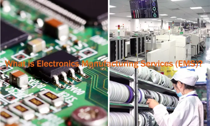
Electronics Manufacturing Services (EMS) power industries ranging from consumer electronics to aerospace, medical devices, and industrial automation. As technology advances, manufacturers are integrating cutting-edge processes such as high-density interconnect (HDI) PCBs, rigid-flex circuits, lead-free soldering, AI-driven quality inspection, and 5G-enabled automation to keep up with evolving market demands.
In EMS, PCB manufacturing involves material selection, signal integrity optimization, and thermal management, while PCB assembly incorporates Surface Mount Technology (SMT) and Through-Hole Technology (THT). High-reliability production requires precise design and strict quality control methods, including In-Circuit Testing (ICT), functional testing, and Environmental Stress Screening (ESS). Additionally, supply chain management plays a central role in global component sourcing, inventory forecasting, and counterfeit component prevention.
This guide delves into the core technologies, cost optimization strategies, and critical factors in selecting the right manufacturing partner, providing OEMs, PCB designers, and manufacturers with a comprehensive industry perspective.
Understanding Electronics Manufacturing Services (EMS) and Its Industry Applications
Electronics Manufacturing Services (EMS) support the design, assembly, testing, and distribution of electronic products across various industries. Companies that rely on EMS providers gain access to advanced manufacturing technologies, streamlined supply chain management, and specialized expertise. From printed circuit board (PCB) assembly to full system integration, EMS providers assist businesses in optimizing production and ensuring product reliability.
Each industry has its own manufacturing needs, regulatory requirements, and production complexities. The right EMS approach depends on factors such as material sourcing strategies, compliance standards, and production volume. A closer look at EMS operations and their role in different sectors provides insight into how companies leverage these services.
What Are Electronics Manufacturing Services (EMS) and Their Core Functions?
EMS providers cover multiple aspects of electronic product development and manufacturing. Their facilities incorporate automated production lines, precision assembly techniques, and quality control systems to handle complex builds. EMS offerings extend beyond manufacturing to include supply chain coordination and post-production support.
Small-batch production runs to evaluate design effectiveness and manufacturability.
Supply Chain Management
Component sourcing, procurement strategies, and inventory control to prevent disruptions.
Testing & Quality Assurance
Inspection processes, including in-circuit testing (ICT), automated optical inspection (AOI), and functional validation.
Box Build & Final Assembly
Integration of electronics into enclosures with wiring, firmware installation, and final testing.
Regulatory Compliance & Certifications
Adherence to industry-specific standards such as IPC-A-610, ISO 9001, RoHS, and ITAR.
Aftermarket & Repair Services
Maintenance, refurbishment, and troubleshooting support for electronic products.
Automated equipment and industry best practices improve consistency across these processes. EMS providers structure production workflows to match client specifications while addressing environmental considerations, design complexity, and performance testing.
How EMS Supports Consumer Electronics, Aerospace, and Medical Device Industries?
EMS providers work with companies across multiple sectors, each with distinct production requirements. Their ability to handle precision manufacturing, compliance mandates, and efficient logistics makes them valuable partners in delivering high-quality electronic products.
Consumer Electronics: High-Volume Manufacturing and Rapid Production Cycles-
Consumer electronics manufacturing prioritizes efficiency, cost management, and fast turnaround times. Devices such as smartphones, gaming consoles, and home automation systems require streamlined production to keep pace with shifting market trends. EMS providers implement automated assembly lines and design-for-manufacturability (DFM) strategies to support these projects.
Key Considerations in Consumer Electronics EMS:
●High-speed SMT placement for miniaturized components.
●Flexible production scaling to accommodate demand fluctuations.
●Efficient prototyping and rapid validation of new designs.
Aerospace & Defense: Compliance and High-Reliability Manufacturing-
Electronics used in aerospace and defense applications must endure harsh environments, extreme temperatures, and electromagnetic interference. EMS providers in this sector follow strict manufacturing guidelines and conduct extensive testing to validate product performance under stress conditions.
Core Considerations in Aerospace & Defense EMS:
●Conformal coating and thermal management solutions for extended durability.
●Multi-stage inspection and quality verification processes.
●Secure supply chain oversight for controlled component sourcing.
Medical Devices: Regulatory Adherence and Precision Assembly-
The medical industry enforces strict regulations to ensure the safety and effectiveness of electronic equipment. EMS providers working in this sector must document every stage of production, maintain cleanroom assembly environments, and comply with international medical standards.
Main Considerations in Medical Device EMS:
●ISO 13485 certification and adherence to FDA guidelines.
●Comprehensive traceability systems for material tracking.
●Electrostatic discharge (ESD) protection measures to prevent component failures.
Each of these industries depends on EMS providers to meet specific production challenges. The choice of an EMS partner should align with the regulatory, technological, and logistical demands of the sector.
Differences Between EMS, ODM, and OEM in Electronics Production
EMS, ODM (Original Design Manufacturer), and OEM (Original Equipment Manufacturer) represent different approaches to electronics production. Understanding their distinctions helps businesses determine the best outsourcing strategy for their needs.
Model
Description
EMS (Electronics Manufacturing Services)
Provides contract manufacturing, PCB assembly, testing, and logistics for various clients.
ODM (Original Design Manufacturer)
Designs and produces electronic products, which other brands can customize and resell.
OEM (Original Equipment Manufacturer)
Develops and markets electronic products under its own brand but outsources production.
Choosing the Right Model for Production Needs-
●EMS providers handle manufacturing without contributing to product design. Companies looking for reliable assembly, testing, and supply chain services benefit from this model.
●ODM companies offer pre-designed solutions that can be modified based on customer requirements. This option is suitable for businesses that want to introduce products with minimal design investment.
●OEMs maintain control over the design and branding of their products while relying on external manufacturing partners for production scalability.
Selecting the appropriate approach depends on production goals, cost considerations, and the level of design involvement required. EMS remains a solution for companies seeking specialized manufacturing support without investing in in-house production infrastructure.
High-Precision PCB Manufacturing in Electronics Manufacturing Services (EMS)
Printed circuit boards are at the center of electronic manufacturing, providing the structural and electrical foundation for everything from everyday consumer gadgets to high-performance aerospace and medical devices. The demand for smaller, more efficient, and more complex circuit boards has led to advancements in fabrication methods, material selection, and quality assurance. EMS providers apply specialized manufacturing techniques to ensure that PCBs meet electrical, mechanical, and environmental requirements while keeping production scalable and cost-effective.
This section explores how EMS companies handle PCB fabrication, the materials used to optimize performance, and the industry standards that define manufacturing quality.
Advanced PCB Fabrication Techniques: HDI, Rigid-Flex, and Multilayer Boards
The push for high-performance electronics has driven PCB manufacturing to evolve beyond standard two-layer designs. Depending on the application, manufacturers incorporate high-density interconnect (HDI) designs, rigid-flex configurations, or multilayer structures to maximize space utilization, improve signal integrity, and enhance durability.
HDI (High-Density Interconnect) PCB Fabrication-
HDI boards allow for finer trace patterns, smaller vias, and increased wiring density, making them suitable for compact and high-speed applications such as telecommunications equipment and advanced computing systems.
Characteristics of HDI PCBs:
●Microvias and laser-drilled holes for compact circuit routing.
●Sequential lamination for high layer count and signal efficiency.
●Optimized stack-ups that reduce electromagnetic interference (EMI).
Rigid-Flex PCB Manufacturing-
Rigid-flex PCBs combine the durability of rigid circuits with the adaptability of flexible substrates. These designs eliminate the need for connectors between different sections of a board, reducing potential failure points and saving space.
Manufacturing considerations for rigid-flex PCBs:
●Layer stacking to balance mechanical flexibility and electrical performance.
●Controlled impedance routing to support high-speed data transmission.
●Precision laser cutting and drilling for clean flex section transitions.
Multilayer PCB Production-
For applications requiring complex signal distribution and power management, multilayer PCBs provide a way to incorporate multiple circuits within a compact design.
Factors influencing multilayer PCB fabrication:
●Material selection for dielectric layers to maintain consistent electrical properties.
●Advanced lamination techniques to prevent internal delamination.
●Copper thickness optimization for efficient current flow.
EMS providers select the appropriate PCB fabrication approach based on product requirements, ensuring durability, efficiency, and manufacturability at scale.
Material Selection for High-Reliability PCBs: FR4, Rogers, and Ceramic Substrates
The materials used in PCB construction affect electrical performance, heat dissipation, and mechanical strength. EMS providers work with a range of substrates to match the needs of specific applications, balancing factors such as frequency stability, thermal resistance, and cost efficiency.
FR4: Standard for General-Purpose PCBs-
FR4 is the most widely used PCB material, offering a combination of electrical insulation, mechanical strength, and affordability. It is commonly found in industrial automation, consumer electronics, and automotive applications.
FR4 Properties
Typical Value
Dielectric Constant (Dk)
~4.2 – 4.8
Thermal Conductivity
~0.25 W/m·K
Glass Transition Temperature (Tg)
130°C – 180°C
Rogers Materials: Designed for High-Frequency Electronics-
For applications requiring low signal loss and improved thermal stability, Rogers laminates provide better electrical performance than traditional FR4. These materials are frequently used in 5G networks, aerospace radar systems, and RF communication devices.
Advantages of Rogers PCB Materials:
●Low loss tangent for reduced signal degradation.
●Stable dielectric constant across temperature variations.
●High-frequency compatibility for microwave and millimeter-wave circuits.
Ceramic Substrates: Thermal Stability and Durability-
Ceramic-based PCBs handle extreme temperature conditions and provide excellent thermal conductivity, making them reliable for power electronics, automotive engine controls, and high-reliability aerospace components.
Why Ceramic Substrates Are Used:
●High resistance to oxidation and moisture exposure.
●Efficient heat dissipation for high-power circuits.
●Low expansion rates, reducing stress on solder joints.
Each material offers unique properties that determine its suitability for different PCB applications. EMS providers assess operating conditions, signal requirements, and production scale to select the best material for a given design.
How EMS Ensures PCB Manufacturing Meets Industry Standards?
PCB manufacturing follows strict guidelines to ensure that boards function correctly and maintain consistency across production batches. EMS providers integrate industry-recognized quality standards and inspection methods to verify that every PCB meets performance expectations before final assembly.
IPC Standards in PCB Manufacturing-
The IPC (Institute for Printed Circuits) establishes globally accepted benchmarks for PCB design, fabrication, and testing. Compliance with IPC standards reduces variability and ensures that manufacturers follow best practices.
IPC Standard
Purpose
IPC-6012
Qualification and performance for rigid PCBs
IPC-2221
Generic design standards for printed circuits
IPC-A-600
Acceptability of printed boards
Testing and Quality Control in PCB Production-
EMS providers conduct multiple rounds of testing to detect defects and confirm that boards function as intended.
●Automated Optical Inspection (AOI): Uses high-resolution cameras to identify issues such as solder bridging and misaligned components.
●In-Circuit Testing (ICT): Checks continuity and component values to verify electrical correctness.
●X-Ray Inspection: Analyzes hidden solder joints, particularly for ball grid arrays (BGAs) and multilayer PCBs.
Regulatory Compliance for Industry-Specific Applications-
Different industries require additional certifications to meet product safety and performance regulations.
●ISO 13485: Required for medical electronics manufacturing.
●IATF 16949: Ensures compliance with automotive industry production standards.
●ITAR Compliance: Necessary for defense and aerospace applications.
PCB Assembly Processes in Electronics Manufacturing Services (EMS)
Building a circuit board is more than just placing components onto a substrate. Every step in the assembly process impacts how well the final product operates in real-world conditions. EMS providers bring together advanced automation, skilled technicians, and strict quality control measures to deliver reliable PCBs for industries such as consumer electronics, aerospace, and medical technology.
Choosing the right assembly method, soldering techniques, and inspection processes ensures that boards can handle high-performance demands while meeting regulatory standards. Let’s break down the most widely used PCB assembly techniques, lead-free soldering advancements, and quality assurance methods that keep production in check.
Surface Mount Technology (SMT) vs. Through-Hole Technology (THT) in EMS
Every PCB design calls for an assembly method that aligns with its application. Two widely used techniques—Surface Mount Technology (SMT) and Through-Hole Technology (THT)—offer different benefits based on factors such as board complexity, durability requirements, and manufacturing scale.
Surface Mount Technology (SMT) Assembly-
SMT has transformed PCB production by allowing smaller, lightweight components to be placed directly onto the surface of the board. With automated pick-and-place machines and reflow soldering, this method supports high-speed manufacturing while keeping costs manageable.
Advantages of SMT in EMS Manufacturing:
●Supports compact, lightweight designs for modern electronics.
●Enables faster, high-volume production through automation.
●Enhances electrical performance by reducing lead length.
SMT Assembly Process in EMS:
Step
Description
Solder Paste Application
A stencil applies solder paste onto PCB pads.
Component Placement
Automated machines precisely position components.
Reflow Soldering
Controlled heat bonds components securely.
Inspection & Testing
AOI and functional tests ensure proper assembly.
Through-Hole Technology (THT) Assembly-
While SMT dominates modern electronics, THT still plays a strong role in applications that demand durable mechanical connections, such as industrial controls and aerospace systems.
When THT Makes Sense:
●Ideal for components handling high currents and voltages.
●Strengthens solder joints for vibration-heavy environments.
●Simplifies repairs and modifications in certain designs.
Common THT Soldering Methods:
Method
How It Works
Wave Soldering
A molten solder wave bonds components efficiently.
Hand Soldering
Used for repairs, prototypes, and specialty components.
Selective Soldering
A precise alternative for mixed-technology boards.
Many EMS providers combine SMT and THT in hybrid PCB designs to balance speed, durability, and cost.
Lead-Free and RoHS-Compliant Soldering Techniques for EMS Manufacturing
Shifting away from traditional lead-based solder has become a priority in electronics manufacturing. With Restriction of Hazardous Substances (RoHS) compliance required in many regions, EMS companies now rely on lead-free solder alloys that meet environmental and performance standards.
Popular RoHS-Compliant Soldering Alloys-
Lead-free soldering brings challenges, such as higher melting points and different wetting properties. The table below highlights commonly used alternatives.
Solder Alloy
Composition
Melting Point (°C)
Why It’s Used
SAC305
Sn96.5/Ag3.0/Cu0.5
217-220
Reliable for most applications.
Sn100C
Sn99.3/Cu0.7
227
Reduces oxidation risks.
Bi57Sn42Ag1
Bi57/Sn42/Ag1
138
Low-temperature option for sensitive components.
How EMS Providers Handle Lead-Free Soldering Challenges-
●Solder Joint Durability: Flux and pad design modifications improve bonding.
As lead-free technology continues evolving, EMS manufacturers refine their processes to meet industry expectations without compromising reliability.
The Role of Automated Optical Inspection (AOI) in EMS PCB Assembly
No matter how advanced a manufacturing process is, errors can still occur. A single misplaced component or poor solder joint can lead to performance issues, product recalls, or safety risks. Automated Optical Inspection (AOI) systems step in to catch these issues before they become bigger problems.
How AOI Works in PCB Manufacturing-
AOI relies on high-resolution cameras, pattern recognition, and machine learning algorithms to inspect every PCB that comes off the assembly line.
●Handles High-Speed Production: Keeps up with automated lines.
●Supports Complex PCB Designs: Inspects fine-pitch components and multi-layer structures.
With AOI acting as a checkpoint, EMS manufacturers can maintain high-quality production standards while reducing waste and improving efficiency.
Design for Manufacturability (DFM) and Design for Assembly (DFA) in EMS
Bringing a PCB design from concept to production isn’t just about getting circuits onto a board—it’s about making sure the design works seamlessly with real-world manufacturing processes. Design for Manufacturability (DFM) and Design for Assembly (DFA) are the foundation of any EMS workflow, ensuring that a product moves through fabrication and assembly without delays, cost overruns, or performance issues.
Companies that overlook these principles often find themselves battling production bottlenecks, excessive scrap rates, or field failures. By considering material choices, layout efficiency, and component selection upfront, EMS providers help us refine their designs for streamlined manufacturing. Let’s dive into the core aspects of PCB layout optimization, common design missteps, and engineering challenges related to high-speed signals and thermal performance.
How EMS Providers Optimize PCB Layout for Cost-Effective Manufacturing?
PCB layout is where good intentions meet real-world constraints. A design that looks flawless on a screen might end up causing unnecessary delays and expenses if it’s not aligned with manufacturing processes. EMS providers help engineers fine-tune layouts so they integrate with standard fabrication techniques, automated assembly, and quality control procedures.
To make production flow without unnecessary setbacks, we focus on several aspects of PCB design:
●Component placement: Parts need to be arranged in a way that allows automated machines to place them accurately and efficiently.
●Trace routing: Poorly designed trace paths can lead to signal integrity issues and added costs during manufacturing.
●Drill hole sizing and spacing: Incorrectly specified holes can cause issues with plating and lead to board failures.
●Panelization strategies: Multiple PCBs are often fabricated in a single panel to improve throughput and reduce waste.
Taking the time to refine these aspects early means fewer production slowdowns, better material utilization, and a smoother transition from prototype to full-scale manufacturing.
Common PCB Design Mistakes and Their Impact on EMS Production
Even the best engineers occasionally overlook factors that affect manufacturing. Some mistakes might not show up until production begins—when it’s already too late to fix them without adding cost and delays.
EMS providers regularly see preventable issues that could have been caught with an early DFM check, such as:
●Mismatched footprints: Components that don’t align properly with the PCB pads can lead to soldering defects.
●Inconsistent trace widths: This can create electrical performance issues, especially in high-speed designs.
●Poor thermal relief design: Incorrect copper connections around component leads can cause soldering inconsistencies.
●Sharp angles in traces: This increases the risk of electrical noise and signal degradation.
●Overlapping copper pours: Unintended shorts can occur, leading to rework or scrapped boards.
Signal Integrity, Thermal Management, and High-Speed Design Considerations
Modern circuit boards are pushing limits in speed, power, and miniaturization. The smaller and denser a board becomes, the more engineers need to pay attention to signal integrity, heat dissipation, and electromagnetic interference.
When it comes to signal performance, trace width, spacing, and layer stack-up all play a role in reducing unwanted noise and ensuring signals reach their destination intact. Poor routing or improper impedance matching can lead to performance drops or even complete circuit failure.
Thermal management is another major factor, especially in designs where power-hungry components are packed into tight spaces. Without the right strategy, heat builds up quickly and can cause instability or shorten the lifespan of electronic devices. EMS providers use a combination of thermal vias, copper thickness adjustments, and heat sinks to keep temperatures under control.
Ignoring these factors isn’t just an inconvenience—it can mean the difference between a reliable product and one that struggles in real-world conditions.
Prototyping and Quality Control in Electronics Manufacturing Services (EMS)
Transforming an electronic idea into a finished product is no simple task. Every step requires meticulous planning, precise execution, and strict validation. Before moving to full-scale production, PCB prototyping and quality assurance ensure a hassle-free transition.
EMS can providers help our engineers fine-tune designs, resolve manufacturing bottlenecks, and confirm performance expectations long before production ramps up. Without these steps, companies risk unexpected delays, excessive costs, and compromised product reliability—headaches no business wants to deal with.
Let’s break down how prototyping, testing, and compliance shape the electronics manufacturing landscape.
Rapid PCB Prototyping: Refining Designs Before Full-Scale Production
Prototyping is where ideas get stress-tested. Engineers get a chance to spot flaws, improve circuit layouts, and confirm electrical performance before committing to large production runs. EMS providers use various methods to keep this process efficient, including:
●Quick-turn PCB fabrication: Accelerates design iterations with rapid manufacturing of prototype boards.
●On-demand assembly services: Allows small-batch PCB assembly with precise component placement, even for fine-pitch and BGA packages.
●Additive manufacturing for test fixtures: Enables quick adjustments to connectors, enclosures, and mechanical parts.
While prototyping saves time and refines designs, we need to consider material compatibility, DFM constraints, and real-world manufacturing limitations. A well-executed prototype prevents unexpected surprises during full-scale production.
PCB Testing Methods: Preventing Failures Before They Happen
No manufacturer wants to deal with field failures, product recalls, or unhappy customers. That’s why EMS providers implement multiple testing strategies to detect design flaws, process inconsistencies, and performance issues before PCBs leave the factory.
●In-Circuit Testing (ICT): Detects component placement errors, shorts, and open circuits at the board level.
●Functional Testing: Simulates real-world operating conditions to confirm PCBs perform as intended.
●Environmental Stress Screening (ESS): Subjects PCBs to temperature fluctuations, vibration, and humidity to assess durability in harsh conditions.
Skipping these steps invites costly rework, delays, and customer dissatisfaction. Thorough testing ensures PCBs meet application requirements and maintain consistent performance over time.
EMS Industry Certifications: Meeting Manufacturing and Regulatory Standards
For EMS providers, compliance is non-negotiable. Certifications demonstrate adherence to manufacturing protocols, process controls, and regulatory requirements across various industries. Some of the most recognized certifications include:
●IPC Standards: Define quality benchmarks for PCB fabrication, assembly, and inspection.
●ISO 9001: Outlines best practices for maintaining consistent production processes and customer satisfaction.
●FDA Compliance: Applies to medical electronics, ensuring devices meet strict safety and performance regulations.
Electronics Manufacturing Services (EMS) and Supply Chain Management
Electronics Manufacturing Services (EMS) isn’t just about building printed circuit boards or assembling electronic devices—it’s about making sure every component, from microcontrollers to capacitors, arrives on time, meets specifications, and stays within budget.
With global supply chains becoming more unpredictable, EMS providers must navigate sourcing challenges, fluctuating lead times, and compliance requirements to keep production lines moving. Companies that fail to adapt to supply chain disruptions risk project delays, unexpected costs, and even lost customers.
Let’s explore how EMS providers handle supply chain risks, leverage AI-driven forecasting, and prevent counterfeit components from infiltrating production.
Managing Global Supply Chain Risks in EMS Manufacturing
The electronics industry has always been at the mercy of market fluctuations, geopolitical events, and material shortages. A single bottleneck—whether it’s a semiconductor shortage or a shipping delay—can send shockwaves through an entire production schedule.
EMS providers tackle these risks by:
●Diversifying suppliers: Relying on a single vendor for critical components is a recipe for trouble. EMS companies maintain a network of alternative suppliers to ensure steady supply.
●Strategic inventory planning: Stockpiling high-risk components and forecasting demand helps prevent last-minute scrambles for parts.
●Regional sourcing strategies: Nearshoring production can cut down on customs delays, tariffs, and transportation costs, keeping things more predictable.
Manufacturers that take a proactive approach to supply chain management can avoid the costly pitfalls that come with last-minute part substitutions, production halts, and rushed redesigns.
The Role of AI in Component Sourcing and Inventory Forecasting
AI is changing the game in how EMS providers source components, predict shortages, and optimize inventory levels. Traditional forecasting methods struggle to keep up with market volatility, but AI-driven solutions offer real-time insights that help manufacturers stay ahead.
Here’s how AI transforms supply chain management in EMS:
●Predictive analytics: AI-powered systems analyze historical purchase data, global supply trends, and real-time demand shifts to flag potential shortages before they happen.
●Automated supplier matching: Instead of relying on manual searches, AI can scan global databases and recommend alternative sources when parts are unavailable.
●Smart inventory control: AI can identify slow-moving stock and optimize reorder points, preventing overstocking or last-minute shortages.
EMS companies that embrace AI-driven supply chain strategies can make smarter purchasing decisions, minimize disruptions, and reduce excess costs tied to poor inventory planning.
Preventing Counterfeit Electronic Components in EMS Supply Chain
Counterfeit electronic components aren’t just a nuisance—they can lead to device failures, warranty claims, and even safety hazards. With counterfeiters getting more sophisticated, EMS providers need strict screening processes to keep fake parts out of their supply chain.
Here’s how EMS providers spot and eliminate counterfeit risks:
●Trusted vendor partnerships: EMS companies work only with authorized distributors and certified suppliers to avoid gray-market parts.
●Advanced component testing: X-ray inspection, decapsulation analysis, and electrical testing help detect counterfeit semiconductors and passive components.
●Blockchain-based tracking: Some companies use digital ledgers to trace components from manufacturer to end product, ensuring authenticity.
A robust anti-counterfeit strategy saves us from costly recalls, brand damage, and potential liability issues. Cutting corners in component sourcing isn’t worth the risk when product integrity is on the line.
Cost Optimization Strategies in Electronics Manufacturing Services (EMS)
Electronics Manufacturing Services (EMS) providers are always on the lookout for ways to reduce expenses while maintaining production standards. Every decision, from PCB manufacturing methods to supply chain efficiency, directly impacts overall costs. Smart planning, material selection, and streamlined logistics can lead to significant savings without sacrificing reliability.
Let’s explore how EMS companies control production costs while ensuring efficiency remains high.
Reducing PCB Manufacturing Costs Without Compromising Quality
Lowering PCB manufacturing costs requires a combination of strategic design, material efficiency, and process refinement. Adjusting panelization, standardizing board sizes, and selecting cost-effective substrates all contribute to savings without causing performance issues down the line.
Approaches to Lower PCB Manufacturing Costs-
Cost Reduction Method
Impact on Expenses
Optimized Panelization
Reduces material waste by increasing board yield
Standardized Board Dimensions
Eliminates custom tooling fees
Bulk Purchasing of Components
Lowers per-unit cost with supplier discounts
Alternative Substrates
Finds balance between material cost and performance
Layer Reduction
Cuts down on manufacturing complexity
By focusing on these adjustments, EMS providers keep manufacturing expenses under control while ensuring PCBs meet performance expectations.
The Advantages of Outsourcing PCB Assembly to EMS Providers
Handing over PCB assembly to an EMS provider helps businesses streamline operations and reduce in-house expenses. With established infrastructure, experienced staff, and access to cost-effective materials, EMS companies handle production more efficiently than many in-house setups.
How EMS Outsourcing Reduces Expenses-
Factor
Effect on Cost
Large-Scale Production
Lowers per-unit costs through high-volume assembly
Skilled Technicians
Removes need for extensive in-house training
Advanced Equipment Access
Avoids investment in costly machinery
Shorter Lead Times
Minimizes storage and holding costs
Established Supply Networks
Reduces component expenses through supplier relationships
By outsourcing assembly, businesses shift focus toward innovation and market growth while keeping production costs manageable.
Just-In-Time (JIT) Inventory Management for EMS Production
Keeping excessive inventory ties up capital, increases storage costs, and raises the risk of component obsolescence. Just-In-Time (JIT) inventory management ensures materials arrive only when needed, cutting down on waste and unnecessary stockpiling.
JIT Inventory Benefits for EMS Providers-
JIT Strategy
Cost Impact
Lower Warehouse Expenses
Reduces the need for large storage facilities
Less Material Waste
Prevents outdated parts from sitting on shelves
Better Cash Flow
Keeps funds available for other operations
Flexible Supply Chain
Allows quicker response to demand changes
With JIT inventory management, EMS manufacturers maintain a lean, efficient operation without unnecessary financial strain.
Choosing the Right Electronics Manufacturing Services (EMS) Partner
Selecting an EMS provider is more than just about production capabilities—it’s about building a long-term collaboration that supports efficiency, quality, and scalability. An effective partnership with an EMS company helps OEMs navigate supply chain challenges, optimize manufacturing costs, and ensure compliance with industry standards.
To make an informed decision, companies need to evaluate technical expertise, production capacity, regulatory compliance, and overall financial impact. Let’s dive into the essential aspects of choosing an EMS partner and how the right selection can streamline product development.
Factors to Consider When Selecting an EMS Provider
Choosing an EMS provider requires a detailed look at production capabilities, supply chain reliability, engineering expertise, and regulatory compliance. Beyond pricing, the ability to meet production demands, ensure consistent quality, and provide technical support can make a significant difference in the long run.
A provider with strong engineering resources can help refine designs, improve manufacturability, and troubleshoot issues before they become costly. Manufacturing capacity should align with both current needs and future scalability. A well-established supply chain network helps prevent delays and secures high-quality components. Certifications such as IPC and ISO indicate adherence to industry standards, ensuring that the final product meets all necessary regulations.
Cost transparency is another major factor. A low upfront cost does not always translate to lower overall expenses. Additional costs can arise from logistics, quality control, or unexpected delays, making it essential to evaluate the total financial impact.
Key Considerations When Evaluating EMS Providers-
Factor
Why It Matters
Engineering Expertise
A strong team can assist in design improvements and DFM/DFA optimization
Manufacturing Capacity
The facility should handle your volume needs, whether for prototypes or mass production
Supply Chain Management
A well-connected provider can reduce lead times and secure reliable components
Compliance and Certifications
Ensures products meet industry regulations (IPC, ISO, FDA, etc.)
Cost Structure
A transparent pricing model prevents unexpected expenses
Flexibility and Scalability
The provider should support future product iterations
By assessing these areas, businesses increase their chances of forming a productive partnership that supports their long-term manufacturing goals.
How EMS Companies Improve Time-to-Market for OEMs?
In electronics manufacturing, keeping up the pace is a big deal. Production slowdowns can mean missed chances, increased expenses, and reduced profits. EMS providers with streamlined operations and well-organized supply chains help businesses launch products faster while ensuring consistent output.
Rapid prototyping services allow OEMs to refine their designs early in the development process, reducing time spent on revisions. Engineering support speeds up problem-solving, preventing design flaws from causing production delays. A well-integrated supply chain keeps components readily available, reducing downtime caused by material shortages. Automation in assembly ensures faster production cycles with greater precision, leading to shorter lead times.
How EMS Providers Shorten Time-to-Market-
Strategy
Impact on Time-to-Market
Rapid Prototyping Services
Helps OEMs test and refine designs quickly
In-House Engineering Support
Speeds up design revisions and problem-solving
Integrated Supply Chain Management
Reduces delays in component sourcing
Automated Assembly Processes
Increases production speed and consistency
By leveraging these strategies, EMS providers help OEMs get their products into the market faster without sacrificing quality.
Understanding the Total Cost of Ownership (TCO) in EMS Outsourcing
When evaluating EMS providers, the quoted price per unit does not always reflect the actual financial impact of outsourcing. The total cost of ownership (TCO) takes into account factors such as logistics, quality assurance, potential rework, and supply chain risks.
Production costs go beyond just assembly—shipping expenses, customs fees, and warehousing costs can add up quickly. If a provider has a high defect rate, expenses related to rework and scrap can outweigh initial cost savings. Delays in sourcing materials or manufacturing setbacks can disrupt product launch schedules, leading to missed revenue opportunities.
Working with an EMS provider that maintains consistent production quality and supply chain reliability helps companies avoid unexpected costs. A careful evaluation of long-term financial impact ensures a stable and cost-effective manufacturing partnership.
Breaking Down TCO in EMS Partnerships-
Cost Factor
Why It Affects the Bottom Line
Unit Price vs. Total Cost
A low per-unit cost doesn’t always mean lower overall expenses
Logistics & Shipping
Long-distance suppliers may lead to higher freight and tariff costs
Late shipments can disrupt entire production schedules
Service & Support Costs
Lack of engineering assistance can lead to expensive design flaws
Understanding TCO prevents companies from making short-term decisions that lead to long-term financial strain.
Emerging Technologies in Electronics Manufacturing Services (EMS)
The electronics manufacturing industry is undergoing a transformation driven by new technologies. EMS providers are adopting advanced manufacturing techniques to improve efficiency, enhance product performance, and meet the growing demand for miniaturized, flexible, and high-speed devices.
The following sections will explore some of the most impactful technological trends shaping the future of EMS.
Miniaturization Trends in EMS: Chip-on-Board and Embedded Components
As electronic devices become more compact, the demand for high-density packaging technologies continues to rise. Traditional component packaging is being replaced with more space-efficient solutions to optimize performance and streamline manufacturing processes.
Chip-on-Board (COB) technology eliminates the need for traditional component packaging by mounting bare dies directly onto the PCB. This approach reduces power consumption, improves heat dissipation, and accelerates signal transmission. Industries such as medical electronics, automotive, and aerospace are increasingly using COB to meet strict size and performance requirements.
Embedded components take integration a step further by incorporating passive and active elements within the PCB layers. This design reduces signal interference, enhances mechanical strength, and enables ultra-thin devices. However, embedded components present challenges in manufacturing, repairability, and design complexity.
As miniaturization advances, many manufacturers are adopting sophisticated inspection techniques such as high-resolution X-ray imaging and automated optical inspection (AOI) to ensure high-density PCB quality.
Flexible and Wearable Electronics: The Future of EMS PCB Design
Flexible electronics are redefining PCB design, enabling lighter, more durable, and adaptable solutions for wearable and foldable devices.
Flexible PCBs (FPCs) use materials like polyimide (PI) and liquid crystal polymer (LCP), allowing circuits to bend without performance loss. These circuits are widely used in foldable smartphones, automotive displays, and smartwatches.
Wearable electronics rely on flexible technology for comfort and long-term usability. Smartbands, medical sensors, and fitness trackers demand high-reliability flexible PCBs that can withstand mechanical stress and environmental conditions. As demand increases, EMS providers are optimizing manufacturing techniques, including advanced adhesives, precision soldering, and high-accuracy component placement.
Manufacturing flexible PCBs presents challenges such as substrate handling, connection reliability, and mechanical stress management. To address these issues, factories are deploying precision robotic arms and automated production lines to maintain high-quality standards.
How 5G and AI Are Transforming the EMS Industry?
The integration of 5G and artificial intelligence (AI) is reshaping the EMS landscape, enhancing automation, and optimizing supply chain operations.
5G technology improves data transmission speeds between machines, enabling real-time analytics and remote-controlled production lines. The low-latency, high-bandwidth connectivity supports smart factory operations, reducing downtime and optimizing resource allocation.
Artificial intelligence is being deployed in automated optical inspection (AOI), predictive maintenance, and supply chain management. For example, AI-driven algorithms can analyze manufacturing data to detect defects early, significantly reducing waste and improving yield rates.
Impact of 5G and AI on EMS-
Technology
Benefits
Typical Applications
5G
High-speed data transfer
Remote equipment monitoring, smart factories
AI
Quality inspection and forecasting
AOI detection, supply chain optimization
AI-driven supply chain management helps EMS providers improve inventory forecasting accuracy and mitigate component shortages. By analyzing market trends and historical data, EMS companies can fine-tune procurement strategies, reducing risks associated with stockouts or excess inventory.
IC substrates form the foundation that connects semiconductor components to complex circuit boards. As industries like AI, IoT, 5G, and high-performance computing (HPC) continue to push for faster and more efficient devices, these substrates help ensure that the final products meet the demands of high performance, reliability, and compact design.
This comprehensive guide offers an in-depth look at the essential elements of IC substrate design, including the materials, manufacturing processes, and the specific technologies that enable them to support advanced packaging solutions such as flip-chip and high-density interconnects (HDI).
Introduction to IC Substrates: The Foundation of Advanced Electronics
In today’s world of high-performance electronics, the term “IC substrate” often doesn’t get the attention it deserves. However, these components are at the heart of advanced PCBs and play an indispensable role in modern electronic systems. As the push for more powerful, compact, and energy-efficient devices continues, the evolution of IC substrate technology will play a huge role in driving innovation.
IC substrates are designed to meet the high demands of advanced electronics by providing the necessary structure, electrical pathways, and thermal management required to ensure reliable and efficient device performance. They serve as the fundamental building block for IC packaging, PCB interconnects, and chip-to-board connections.
What is an IC Substrate? Defining Its Role in Electronics?
At their core, IC substrates are multi-layered boards used in PCB design that support integrated circuits (ICs). They provide the physical structure needed to create the electrical connections between the chip and the board, allowing for communication with other components in a system. More than just a base for the IC, these substrates are designed to ensure the smooth transmission of signals and to maintain the thermal balance of the system.
When you think about a smartphone or a 5G base station, the IC substrates inside these devices serve as the foundation for the components that make these devices function. For example, the IC substrate in a 5G base station has to be capable of handling high-frequency signals with minimal signal loss. In the case of AI chips, the IC substrate needs to ensure that the signals passing through it don’t degrade, keeping high-speed data transfer efficient and reliable.
Key Characteristics of IC Substrates in Modern Electronics
When we talk about IC substrates, there are a few standout features that truly define how these components perform in today’s high-demand applications. Let’s break down these main characteristics:
●Signal Integrity: For IC substrates to function effectively, they must maintain signal clarity. This is especially true for high-speed applications like AI chips and HPC systems, where even the smallest distortion in signal quality can lead to significant performance loss. Substrates need to support fast signal transmission without interference, and this requires careful material selection and precise routing.
●Thermal Management: As electronic devices become increasingly powerful, heat management has become a top concern in design. IC substrates are engineered with thermal control in mind, utilizing materials like ceramics or high-performance polymers that efficiently dissipate heat. Take AI processors, for example—they can generate a lot of heat, and without effective heat management, performance could drop off quickly. That’s where thermal vias and heat sinks come into play. These components are built into the substrate to channel heat away from critical parts, ensuring the system stays within the optimal operating temperature and continues to perform at its best.
●Reliability and Durability: The modern demand for long-lasting devices that can operate in challenging environments (such as extreme temperatures, moisture, or mechanical stress) has driven the development of more reliable IC substrates. High-end PCBs and IC substrates need to endure rigorous conditions without degrading, ensuring that systems perform well over extended periods of time.
Why IC Substrates Are Important for Cutting-Edge Technologies?
As electronics continue to evolve, IC substrates are becoming the foundation that enables these advancements. In this section, we’ll explore how IC substrates support some of the most cutting-edge technologies.
●AI and Machine Learning: The rise of AI technologies has led to an increased demand for high-performance processors that can handle complex calculations at scale. IC substrates in AI processors must be capable of supporting high-density connections and rapid data transfer while keeping heat under control. Substrates need to integrate fine-pitch designs and multiple signal layers to meet the high demands of machine learning and neural network processing.
●5G and Next-Gen Networks: As 5G technology expands, the need for robust IC substrates grows. These substrates must support high-frequency signals and high-density interconnections to maintain the speed and efficiency of next-gen communication networks. With 5G base stations and smart devices requiring precision and reliability in signal processing, IC substrates ensure these devices can meet demanding network requirements without performance degradation.
●High-Performance Computing (HPC): Systems designed for high-performance computing often feature multiple processors that run intensive computations. To achieve this level of performance, IC substrates are designed to manage high thermal loads and ensure signal fidelity across multiple processing units. Whether in cloud data centers or scientific research computing, these substrates play an integral role in ensuring that the system runs effectively under pressure.
Materials for IC Substrates: Choosing the Best for High-Performance Applications
In the design of IC substrates for high-performance electronics, selecting the right material can significantly influence the final product’s overall effectiveness. The decision goes beyond just cost; it’s about ensuring that the substrate provides the necessary characteristics like signal integrity, thermal management, and mechanical support for the application at hand.
IC substrates must be tailored to meet specific performance demands. AI processors require fast data processing with efficient power distribution, while 5G systems need materials that ensure low latency and consistent signal transmission. As technology pushes the boundaries of what’s possible, new materials and methods are continually developed to meet these evolving requirements. Let’s delve into the two broad categories of materials used for IC substrates and how their properties directly affect performance.
Organic vs Inorganic Materials: Understanding IC Substrate Materials
In the selection of IC substrate materials, two broad categories stand out: organic and inorganic materials. Each type is chosen based on the demands of the specific application and the environment in which the device will operate.
●Organic Materials (e.g., ABF Resin): Organic substrates, such as those made from ABF (Ajinomoto Build-up Film) resin, are often used in consumer electronics and mid-range devices. These materials are flexible, cost-effective, and allow for high-density interconnects that are often required in modern electronic devices. ABF resin, for example, enables designs with fine-pitch connections and is effective in handling moderate thermal performance. This makes it a preferred choice for IoT devices and smartphones, where power consumption and miniaturization are prioritized.
●Inorganic Materials (e.g., Glass Substrates): Inorganic materials, like glass substrates, are known for their excellent thermal conductivity and dimensional stability, making them a solid choice for applications involving high temperatures and intense workloads. Glass substrates are commonly used in high-performance computing (HPC) systems and 5G infrastructure, where their ability to handle high-frequency signals and manage heat effectively supports smooth operations. These materials help maintain signal integrity and facilitate reliable data transfer, even in demanding environments.
Here’s a comparison table to summarize these materials:
Material Type
Typical Applications
Advantages
Key Characteristics
Organic (ABF Resin)
Consumer electronics, IoT devices
Flexible, lower cost, high-density routing
Fine-pitch designs, moderate thermal performance
Inorganic (Glass)
HPC systems, 5G infrastructure
High thermal conductivity, excellent signal integrity
Signal stability, high-frequency handling
High-Performance Materials for AI and IoT IC Substrates
With the increasing complexity of AI and IoT devices, material selection plays a large part in determining how well these systems operate. The materials used in IC substrates for these applications need to manage high-density interconnections and maintain efficient power distribution while ensuring that signal integrity is preserved under demanding conditions.
●AI Chips: For AI systems, which involve tasks like deep learning and neural networks, IC substrates must handle high-speed data processing without overheating. Materials such as polyimide and ABF resin are frequently used due to their ability to withstand high-frequency signals and thermal loads. These materials help to ensure low signal loss and maintain reliable communication between the various processing units within the AI chip.
●IoT Devices: IoT devices—ranging from smart sensors to wearable tech—require IC substrates that facilitate low power consumption while supporting multiple communication protocols. Materials like FR4 are commonly used in less demanding IoT applications, as they balance cost and performance. However, for industrial IoT or smart city applications, higher-end materials like ceramic substrates or polymides may be used to meet the demands of durability and stability in fluctuating temperatures and environments.
How Material Selection Affects Thermal Management and Signal Integrity?
When designing an IC substrate, thermal management and signal integrity are among the main factors in selecting materials. Each material has specific properties that impact how well the substrate addresses these aspects.
●Dielectric Constant: The dielectric constant of a material governs how it interacts with electrical signals. A material with a low dielectric constant is preferable when signal integrity is a primary concern, especially for high-speed systems like 5G and HPC applications. Lower dielectric constants reduce signal loss and prevent interference, allowing for more precise and faster data transmission.
●Thermal Conductivity: As electronic systems, particularly AI chips and HPC systems, produce significant amounts of heat, the ability to dissipate heat efficiently becomes necessary. Inorganic materials, like ceramics, have higher thermal conductivity, which helps in transferring heat away from sensitive components. This can prevent issues like thermal throttling, where components reduce performance due to excessive heat. On the other hand, organic materials tend to have lower thermal conductivity and are more suitable for applications where heat management isn’t as challenging.
●Signal Loss: Signal loss is another factor that influences IC substrate performance. Materials with low signal loss are preferred in high-frequency systems, such as 5G, where clear signal transmission is needed for smooth data flow. Ceramics are often chosen for these applications due to their low attenuation properties, helping to maintain the strength and quality of high-speed signals.
Here’s a summary of material properties that affect performance:
IC Substrate Manufacturing Processes: Precision Engineering for Performance
The manufacturing of IC substrates is a highly specialized process requiring advanced techniques to achieve the precision necessary for high-performance electronics. As devices get more complex, we must employ increasingly sophisticated methods to create substrates that can handle the demands of AI, IoT, and high-speed data transmission.
The manufacturing process must consider several factors, including the material selection, the complexity of the substrate design, and the precision required for producing microvias, fine-pitch traces, and stacked layers. These processes need to deliver substrates that meet the most stringent standards for signal integrity, thermal management, and mechanical durability. Let’s explore how these advanced manufacturing techniques come together to create high-performance IC substrates that support today’s innovative technologies.
Advanced IC Substrate Manufacturing Techniques
Manufacturing IC substrates involves a series of detailed processes to ensure optimal performance at the smallest scales. Techniques like microvia drilling, etching, stacking, and layer bonding are used to create high-density designs that support advanced electronic circuits.
●Microvia Drilling: One of the most main processes in modern IC substrate production is microvia drilling. These microscopic holes are created to facilitate high-density interconnections within the substrate. Typically, microvias range in size from 50 to 150 microns in diameter and are essential for connecting multiple layers of the substrate while keeping the footprint small. This drilling is done with precision lasers, ensuring minimal thermal stress and maximum control.
●Etching: Etching involves the use of chemical processes to remove unwanted materials and create the intricate patterns required for signal routing on the substrate. By exposing the material to acid-based solutions, we can create circuit patterns that serve as the path for electrical signals. The etching process needs to be extremely controlled to avoid defects that can compromise performance, particularly when working with fine-pitch designs.
●Stacking and Layer Bonding: As substrates become increasingly complex, the need for stacked layers has risen. Stacking involves bonding multiple layers of material to create substrates with higher component density. This allows for multilayer interconnections and ensures that each layer can handle specific electrical tasks. The bonding process requires precision, especially when combining different materials, such as organic films with inorganic layers like glass.
These processes work together to create IC substrates that can handle the intense demands of modern electronic systems. The combination of layering, microvias, and etching provides the structural integrity needed for applications like 5G, AI, and HPC.
The Role of Automation in IC Substrate Production
The growing complexity of IC substrates has made automation a fundamental part of the production process. With the use of machine learning and robotics, automation is transforming how substrates are produced, improving precision and efficiency while reducing the risk of human error.
●Machine Learning in Manufacturing: Machine learning has found its way into PCB manufacturing to predict and improve processes. By analyzing data from production runs, these systems can identify patterns, optimize workflows, and predict maintenance needs. This helps ensure that production remains smooth and cost-effective while maintaining the high standards required for high-performance IC substrates.
●Robotics and Automation Systems: Robotics are used to handle tasks like material handling, inspection, and soldering with unparalleled precision. These automated systems significantly enhance the speed and efficiency of processes like stacking, bonding, and layer alignment. They also allow for much finer control during processes like microvia drilling or etching, ensuring consistency across batches and reducing the chance of defects.
●AI for Predictive Maintenance: Automation also extends to predictive maintenance. With AI-powered tools monitoring every step of the production process, manufacturers can identify potential issues before they arise. For example, soldering issues or material wear can be detected early, minimizing downtime and enhancing overall production efficiency.
The combination of automation and AI brings a new level of precision to IC substrate production, ensuring high yields, reduced waste, and consistent product quality.
Achieving Fine-Pitch Designs for Complex IC Substrates
As electronics advance, fine-pitch designs are becoming more common, especially in high-density IC substrates. Fine-pitch designs involve reducing the distance between interconnects and traces to less than 0.5 mm. These designs are ideal for applications such as AI chips, 5G systems, and HPC, where efficient data transfer and compact sizes are required.
●Fine-Pitch Routing: Fine-pitch routing involves the creation of tight interconnections between microvias and traces. This requires precision etching and careful planning to prevent signal interference or cross-talk. We must also account for thermal expansion and ensure that the substrate maintains its integrity over time as temperatures fluctuate.
●Via-in-Pad: One of the techniques used in fine-pitch design is via-in-pad technology. This technique places vias directly under component pads to allow for tighter spacing, which is particularly useful in high-density circuits. While this method provides more room for component placement, it requires careful handling during soldering and stacking processes to avoid defects.
●Microvia Designs: Microvias are used to route signals through multi-layer substrates, creating a compact layout for high-performance chips. These vias can be blind or buried, depending on the design requirements, and their precise creation helps ensure signal integrity and thermal conductivity are maintained. Microvia designs assist us in achieving the miniaturization needed for next-gen devices while preserving performance and durability.
Table: Comparison of Fine-Pitch Techniques
Design Method
Use Case
Benefits
Challenges
Fine-Pitch Routing
High-speed, miniaturized circuits
Space efficiency, high-density routing
Signal interference, trace complexity
Via-in-Pad
High-density PCBs
Tighter component placement
Potential soldering issues, complexity
Microvia Designs
Multi-layer IC substrates
Minimizes signal loss, supports miniaturization
Manufacturing complexity, cost increases
IC Substrate Design for High-Speed Communication and AI Chips
When designing IC substrates for high-speed communication systems, such as those used in 5G or high-performance computing (HPC), or for AI chips, the stakes are high. These applications demand precision and reliability, as they operate under conditions where signal integrity, thermal management, and electromagnetic interference (EMI) can all make a huge difference in performance.
As the complexity of these chips increases, so does the need for innovative IC substrate designs that address unique challenges. For instance, AI chips typically require tight signal traces and minimized latency, while high-speed circuits like those used in 5G need to handle high frequencies and high power dissipation. Let’s break down the main design aspects and their specific applications to meet these demands effectively.
Signal Integrity in IC Substrates for High-Speed Applications
Signal integrity is one of the most pressing concerns when designing IC substrates for high-speed applications like 5G, HPC, and AI chips. At these frequencies, even the slightest imperfections in the substrate or the traces can cause signal loss or interference, resulting in data corruption or performance degradation. Here’s how impedance matching and crosstalk reduction come into play to keep things running smoothly.
●Impedance Matching:Impedance matching is a technique used to align the electrical impedance of PCB traces with the source and load impedance. This helps to avoid signal reflection, which can cause degradation or distortion, especially at high frequencies. For AI chips or 5G circuits, where maintaining signal clarity is necessary, accurate impedance matching ensures that the signal stays clean and undistorted from the transmitter to the receiver. Achieving this requires the use of advanced simulation tools and precise trace width calculations in the design process.
●Crosstalk Reduction: When multiple signals are routed in close proximity on a substrate, they can interfere with each other, a phenomenon known as crosstalk. For high-speed data transmission, this interference can significantly affect signal integrity. To minimize crosstalk, designers often employ techniques like shielding, ground planes, and the proper spacing between signal traces. By ensuring that trace layouts are properly optimized, crosstalk is reduced, allowing AI chips or HPC systems to operate without data corruption or performance hits.
Table: Key Techniques for Enhancing Signal Integrity in High-Speed Substrates
Technique
Purpose
Application
Benefit
Impedance Matching
Prevent signal reflection and distortion
AI, 5G, HPC circuits
Maintains signal fidelity, prevents data loss
Crosstalk Reduction
Minimize interference between signals
AI chips, high-speed circuits
Enhances signal clarity, reduces errors
Ground Planes
Isolate signal traces and reduce noise
5G, high-speed communications
Improves signal quality, reduces EMI
Thermal Management Strategies in IC Substrate Design
As AI chips and 5G systems operate at increasingly high frequencies, thermal management becomes a challenge. High-frequency chips generate heat, which must be dissipated efficiently to ensure reliable performance over time. Here are some strategies used to control heat and maintain optimal substrate performance:
●Thermal Vias: Thermal vias are small holes within the IC substrate that provide a direct path for heat to travel from one layer to another. This process is used to guide heat away from core components and distribute it more evenly across the board. By using multi-layer designs with thermal vias, heat dissipation is maximized, helping to prevent overheating and component failure in high-power circuits.
●Heat Sinks: Heat sinks are passive devices designed to absorb and dissipate heat generated by high-power components. These are often placed on top of components like power transistors or AI processors to reduce the amount of heat building up within the substrate. In combination with thermal vias, heat sinks are highly effective in managing thermal stress and ensuring long-term reliability of the substrate.
●Thermal Conductivity of Materials: The material selected for the IC substrate impacts the efficiency of heat management. Materials such as ceramics and advanced polymers, known for their high thermal conductivity, are often used to enhance heat distribution. This ensures that even under heavy workloads, the substrate stays within thermal limits, preventing potential issues like thermal runaway or damage to components.
Example Case: In a 5G base station, the heat dissipation needs are particularly high due to the high-speed signal processing required. Our engineers design the substrate with advanced thermal vias and metal-core PCBs, which help rapidly dissipate heat to prevent the 5G chip from overheating during peak usage.
Minimizing Noise and Enhancing Reliability in IC Substrate Designs
Noise and reliability issues in IC substrates can undermine performance, especially for demanding AI and high-speed circuits. Electromagnetic interference (EMI) can degrade signal quality and introduce errors in data transmission. Let’s dive into how noise reduction strategies and reliability-enhancing techniques work together to ensure consistent performance over time.
●Electromagnetic Interference (EMI) Shielding: EMI shielding is one of the most effective ways to minimize external noise that can disrupt signal transmission within an IC substrate. Therefore, many designers use various shielding techniques such as conductive layers and ground planes to block unwanted electromagnetic waves. These shielding structures prevent interference from nearby components, ensuring that AI processors and high-speed communication chips operate without degradation.
●Material Selection for Reliability: Choosing the right materials for IC substrates has a direct impact on the reliability of high-speed circuits. Materials like polyimide, ABF resin, and ceramic composites provide mechanical stability and thermal resistance, ensuring the substrate can withstand extended usage. Reliability tests, such as thermal cycling and mechanical stress tests, are commonly conducted to confirm that the substrate maintains its performance over time.
●Via and Pad Design: The design of vias and pads on the substrate directly impacts its reliability. Via-in-pad designs are used to improve component placement density while ensuring that the vias are robust enough to handle thermal and electrical stresses. The careful pad design ensures proper soldering and electrical connectivity, reducing the chance of failure during long-term use.
Challenges in IC Substrate Design
The design and manufacturing of IC substrates for high-performance circuits require precise engineering and meticulous attention to detail. Challenges like signal integrity, thermal management, and reliability testing need to be addressed effectively to ensure long-lasting performance in diverse applications.
In this section, we’ll explore the common challenges that arise during IC substrate design, including how to address issues related to signal integrity, thermal stresses, and advanced testing for substrate reliability.
H3: Overcoming Signal Integrity Issues in IC Substrate Design
Signal integrity is a fundamental aspect of IC substrate design. As devices become smaller and more powerful, ensuring the quality of high-frequency signals traveling through dense circuits is a growing challenge. Without proper management, issues like signal degradation, impedance mismatch, and noise interference can degrade overall performance, especially in high-speed applications.
To maintain signal quality, several techniques are employed:
●Impedance Matching: It’s essential to design traces with controlled impedance to ensure that signals travel through the substrate without significant reflection. Misaligned impedance leads to signal loss or distortion.
●Crosstalk Reduction: Using ground planes and shielding techniques helps mitigate electromagnetic interference (EMI) and crosstalk between adjacent signals.
●Signal Path Optimization: Shortening the signal paths and optimizing the routing of traces can reduce the loss of high-frequency signals.
As seen in Table 1, choosing the right material is core to achieving low signal loss and optimal impedance control for high-frequency applications.
Addressing Thermal and Mechanical Challenges in IC Substrate Manufacturing
Thermal management is a major factor in IC substrate design. As the demand for higher performance in smaller spaces increases, IC substrates must be able to handle greater heat generation and mechanical stresses without compromising performance.
●Thermal Cycling: Repeated exposure to thermal cycles can cause substrates to expand and contract, leading to delamination and warping. To reduce this risk, high thermal conductivity materials are used to dissipate heat efficiently.
●Mechanical Stress: As substrates become smaller and more densely packed with components, warping or cracking can occur under mechanical strain. Employing reinforced materials or multi-layer designs can help prevent structural failures.
Table 2 compares materials commonly used for IC substrates based on their thermal conductivity and coefficient of thermal expansion (CTE). The higher the thermal conductivity, the better the material is at dissipating heat, while a lower CTE reduces the risk of thermal stress and warping.
Advanced Inspection and Testing for IC Substrate Reliability
Ensuring the reliability of IC substrates is essential to avoid system failures during product lifecycles. Advanced inspection and testing methods help identify flaws that could compromise substrate performance.
●Automated Optical Inspection (AOI): This technology uses high-resolution cameras and image recognition algorithms to detect surface defects such as misaligned vias, cracks, or voids.
●X-ray Inspection: Internal defects that can’t be detected by surface inspection methods can be identified with X-ray imaging, which allows for inspection of the substrate’s inner layers and connections.
●Failure Analysis: Once potential defects are identified, failure analysis tools such as scanning electron microscopy (SEM) and focused ion beam (FIB) help engineers pinpoint the exact cause of the problem.
Table 3: Testing Methods and Defect Detection Capabilities
Testing Method
Defects Detected
Detection Rate
Automated Optical Inspection (AOI)
Surface defects (misalignment, trace breaks)
90%
X-ray Inspection
Internal defects (voids, soldering issues)
95%
Scanning Electron Microscopy (SEM)
Microscopic defects (delamination, cracks)
98%
Focused Ion Beam (FIB)
Internal and surface defects (layer misalignment, pinholes)
99%
In Table 3, we compare inspection techniques based on their ability to detect various types of defects and the detection rate for each method. This provides insight into how us ensure IC substrate reliability during the production process.
Advanced Packaging Techniques for IC Substrates
In the modern electronics manufacturing industry, IC substrates are central to the development and performance of advanced packaging techniques. These techniques drive the compactness and efficiency of high-performance chips used in industries such as AI, 5G, and automotive electronics. The packaging process ensures that the IC substrate can meet the electrical and mechanical demands of modern applications, including high-speed data transfer and thermal management.
To achieve these demands, various packaging strategies are employed, including flip-chip, BGA, HDI, and even 3D packaging. These processes allow for enhanced signal integrity, reduced size, and better thermal conductivity. Let’s dive into some of the most effective packaging techniques and how IC substrates help meet the increasing demand for compact, high-performance electronics.
IC Substrates in Flip-Chip and BGA Packaging
When you look at modern electronics, flip-chip and BGA (Ball Grid Array) are two of the go-to packaging methods used to create compact, high-density circuits. These packaging methods are designed to handle the increasing demand for high-speed signals and reduced form factor, and both leverage IC substrates as the foundation for their performance.
●Flip-Chip Packaging: Flip-chip technology is widely used for its ability to enhance electrical performance by connecting the IC chip directly to the substrate with solder bumps. This design removes the need for wire bonds, which helps save space and shortens electrical paths. In devices like AI chips and 5G components, where clear signals and high-frequency operations are required, flip-chip technology minimizes signal loss and lowers parasitic inductance. IC substrates in flip-chip packages also assist in managing thermal stress, helping the chip function consistently during long operational hours.
●BGA Packaging: BGA packaging involves placing a grid of solder balls on the bottom of the IC substrate, which are then used to connect the chip to the PCB. It’s a widely used method in high-performance computing and mobile devices because it allows for more robust connections and better heat dissipation. With BGAs, the IC substrate provides a reliable interface that facilitates high-speed signal transmission while handling the heat generated by high-performance components.
Table: Key Packaging Techniques and Their Benefits
By using IC substrates, both flip-chip and BGA packaging can enhance the performance and reliability of chips, which is particularly beneficial for industries that demand advanced processing power, such as AI and 5G communications.
IC Substrate Solutions for High-Density Interconnects (HDI)
High-Density Interconnect (HDI) technology makes it possible to integrate more features into smaller spaces. HDI is a transformative method for creating compact, high-performance PCBs and IC substrates found in devices like mobile phones, wearables, and automotive electronics. Through the use of microvias and fine-pitch routing, HDI designs improve signal routing and enhance electrical performance in tightly packed systems.
●Microvia Technology: Microvias are tiny holes drilled into IC substrates to create connections between different layers in a PCB. They’re essential for high-density designs, enabling high-speed signal transmission in compact devices like smartphones and AI chips. The small size of these vias shortens the signal travel distance, which improves signal quality and reduces interference. In AI applications, where fast data processing is necessary, microvias help build dense interconnections while maintaining performance.
●Fine-Pitch Routing: Fine-pitch routing involves placing components with smaller spacing, enabling dense circuit designs. This approach allows IC substrates to support more components in a compact space, maintaining high-speed performance. The design ensures that signal paths remain short, minimizing signal loss and crosstalk, which could otherwise affect performance.
●HDI and AI Chips: For AI applications, HDI substrates ensure that AI chips with numerous connections function smoothly and responsively. These substrates support high-speed processing and manage complex data flows while helping with heat regulation.
Example Case: In an AI-driven autonomous vehicle, the IC substrates using HDI technology must support advanced processing and high-frequency communication without taking up too much space. Microvias ensure that the substrate can hold enough powerful ICs while ensuring signal quality and thermal dissipation.
3D Packaging and Hybrid Materials in IC Substrates
With the growing need for faster chips and higher densities, 3D packaging has emerged as a promising technology to take IC substrates to the next level. This innovation allows multiple layers of chips to be stacked on top of each other, significantly reducing the footprint of the substrate and enabling the miniaturization of electronic devices. Additionally, the use of hybrid materials in IC substrates enhances their overall thermal performance and signal integrity.
●3D Packaging: This technique involves stacking multiple ICs on top of each other in a vertical arrangement. The substrate acts as a support for each layer of chips, with micro-bumps providing connections between the layers. This allows for high-bandwidth data transfer between the stacked chips without significant signal degradation. For AI and HPC applications, 3D packaging offers a compact yet powerful solution for meeting the high-performance needs of next-gen computing systems.
●Hybrid Materials: Hybrid materials such as ceramic-filled polymers or graphene composites are increasingly being used in IC substrates to enhance thermal conductivity and signal integrity. These materials help manage heat more effectively, ensuring that chips in high-performance systems, such as 5G and AI applications, stay within operational temperature limits. Additionally, the versatility of these materials enables the design of more flexible packaging, which is especially beneficial in systems that demand curved or adaptable substrates.
●Integrating Flexible Materials: Another core innovation is the integration of flexible materials into IC substrates. This is particularly beneficial for applications like wearable electronics or flexible displays, where rigid PCB designs don’t work. The use of flexible substrates in combination with advanced packaging techniques allows for the creation of bendable or foldable devices without compromising on signal integrity or thermal performance.
Example Case: A next-gen AI chip designed for edge computing might require a 3D stacked configuration to maximize performance while reducing thermal stress. The IC substrate is designed with hybrid materials to ensure that heat generated by the stacked chips is efficiently managed.
IC Substrates vs. Substrate-Like PCBs (SLP), HDI, and Standard PCBs: A Comparative Analysis
The world of printed circuit boards is vast, and understanding the differences between IC substrates, Substrate-Like PCBs (SLP), HDI (High-Density Interconnect), and standard PCBs is essential for anyone working with high-performance electronics. These types of boards serve different purposes and are designed to meet specific requirements based on application needs, but what sets them apart?
This section will dive into the technical specifications of each type, comparing their design, layer count, thickness, and manufacturing characteristics. We’ll take a closer look at how these differences impact performance, particularly in cutting-edge fields like semiconductor packaging, 5G, AI, and IoT. By the end of this comparison, you’ll have a clearer picture of how to select the right PCB for your next project.
IC Substrates, SLP, HDI, and Standard PCBs: Key Differences in Design and Manufacturing
Let’s break down the distinctions between IC substrates, SLP, HDI, and standard PCBs, focusing on the number of layers, thickness, line width, and spacing—parameters that influence how these boards perform in different applications.
1.Layer Count and Complexity-
●IC Substrates typically range from 2 to 10 layers, designed with precision for semiconductor packaging.
●SLP also falls within 2-10 layers, but with a focus on reducing size and improving signal integrity while accommodating various active and passive components.
●HDI PCBs generally have 4 to 16 layers and are designed to handle high-speed signals with minimal interference, perfect for applications like mobile devices and advanced computing.
●Standard PCBs can stretch the layer count over 100 layers in some cases, depending on the complexity of the circuit. These are often used in traditional consumer electronics but are less suited for high-performance, high-speed designs.
2.Thickness Variations-
●IC Substrates are the thinnest of the group, often coming in at below 1.5mm, with some designs reaching as thin as 0.1mm.
●SLP boards are generally thicker than IC substrates but not as thick as HDI. Their thickness typically falls between 1.5mm and 3mm.
●HDI boards are thicker than SLP substrates, often ranging from 0.4mm to 7mm depending on the complexity and requirements of the end application.
●Standard PCBs can exceed 7mm in thickness, accommodating large, complex circuits or more rugged designs for industrial use.
3.Line Width and Spacing-
●IC Substrates are designed with line widths typically below 25μm (1mil), ideal for high-density designs where signal integrity is a top concern.
●SLP substrates offer a slightly more relaxed design but still support high-density routing with line widths above 1mil (typically in the range of 20-35μm).
●HDI PCBs are designed with line widths around 2mil (50μm), which allows for more complex routing and denser circuit designs compared to standard PCBs.
●Standard PCBs are the least dense in terms of line width and spacing, with widths typically above 2mil and limited to traditional designs with less compact routing.
Table 1: Comparison of Layer Count, Thickness, and Line Width for IC Substrates, SLP, HDI, and Standard PCBs
PCB Type
Layer Count
Thickness
Line Width
Application
IC Substrates
2-10 layers
<1.5mm
<25μm (1mil)
Semiconductor packaging, high-performance chips
SLP (Substrate-Like PCB)
2-10 layers
1.5mm – 3mm
20/35μm
Active/passive components, precision electronics
HDI PCBs
4-16 layers
0.4mm – 7mm
40-50μm
High-speed communication, mobile devices, medical electronics
Standard PCBs
>100 layers
>7mm
>2mil
Consumer electronics, industrial equipment
●Analysis: This table offers a clear comparison of the layer count, thickness, and line width differences across various PCB types. These factors directly influence the choice of substrate based on the specific requirements of your application.
Technical Details of Substrate-Like PCB (SLP) and Its Role Between IC Substrates and HDI
SLP, also known as Substrate-Like PCB, has gained recognition for bridging the gap between IC substrates and HDI boards. Positioned between the two, SLP offers a balanced solution, allowing manufacturers to take advantage of smaller line widths and higher-density routing without fully embracing the complexity of HDI.
●Line Width and Spacing: One of the most significant advantages of SLP is its ability to reduce line width and spacing compared to standard HDI boards. While HDI typically supports line widths around 40-50μm, SLP can bring this down to as low as 20-35μm, allowing for denser routing and more compact designs.
●Design Flexibility: SLP’s ability to support smaller pitches and reduced trace widths makes it an attractive choice for high-performance consumer electronics, mobile devices, and wearable tech. It allows us to pack more functionality into smaller form factors, all while maintaining high reliability.
Table 2: SLP vs. HDI – Line Width Comparison-
PCB Type
Line Width (μm)
Trace Pitch (μm)
Minimum via size (μm)
SLP
20/35μm
30μm
60μm
HDI
40-50μm
50μm
80μm
●Analysis: As demonstrated in Table 2, SLP allows for smaller line widths and tighter trace pitches compared to HDI boards, making it a more cost-effective solution for high-density applications that don’t require the full complexity of HDI design.
IC Substrates vs. SLP, HDI, and Standard PCBs: Use Cases and Applications
Grasping the technical specifications is just one piece of the puzzle. It’s also necessary to align the right PCB type with the specific needs of the application. Below are some industries and use cases where each type of PCB is commonly applied:
●IC Substrates: Typically used in high-performance semiconductor packaging for chips, IC substrates are designed to meet the high-speed and low-volume requirements of advanced electronics. They are good for cutting-edge processors, memory modules, and 3D packaging.
●SLP (Substrate-Like PCB): With its higher density and flexibility, SLP is used in consumer electronics, smartphones, and wearable devices. Its ability to accommodate a variety of active and passive components makes it a go-to choice for compact yet high-performance boards.
●HDI PCBs: These boards are essential in high-speed communication systems, including 5G infrastructure, medical devices, and automotive electronics. Their superior signal integrity makes them perfect for applications where performance is non-negotiable.
●Standard PCBs: Standard PCBs are commonly used in traditional consumer electronics, home appliances, and industrial equipment. They’re the go-to choice when design complexity and speed aren’t the top considerations.
Why Choose Us for Fabricating Your IC Substrates PCB Project?
When it comes to fabricating IC substrates, achieving precision and performance is what sets your project up for success. Whether you’re in semiconductors, telecommunications, high-performance computing, or consumer electronics, selecting the right partner for PCB fabrication makes a real difference. We stand out in the competitive landscape by offering advanced technology, extensive experience, and a proven history of delivering high-quality IC substrates tailored to your specific needs.
1.Expertise in Advanced IC Substrate Designs and Manufacturing
With years of experience in the field, our team brings deep technical knowledge to every project. We specialize in signal integrity, thermal management, and high-density interconnects, ensuring your IC substrates perform as expected under varying conditions.
●Tailored Solutions: We can customize your IC substrates to fit everything from single-chip packaging to complex multi-layer designs, making sure each component functions seamlessly.
●Precision Engineering: We know how much of a challenge it can be to deal with signal loss, impedance mismatch, and the wear and tear caused by thermal cycling in your designs. That’s why we use the latest tools and tech to deliver the precision and reliability you need to keep things running at their best.
2.High-Performance Standards for Various Applications
Our IC substrates are designed to meet the demands of a wide array of high-tech applications. From 5G infrastructure to AI technologies, we build substrates that support the diverse needs of industries looking to stay ahead of the curve.
●5G Technology: We design substrates that are optimized for high-frequency and low-latency applications, ensuring your equipment works efficiently in 5G networks.
●AI and Machine Learning: As AI systems push boundaries, we provide IC substrates that are built to handle high-speed data processing while also maintaining thermal efficiency.
●Medical and Automotive Industries: With a focus on durability and reliability, our IC substrates provide stability and protection against electromagnetic interference, offering assurance in core applications.
3.Advanced Manufacturing Techniques for Maximum Precision
Our production capabilities cover everything from microvia drilling to laser etching, and we rely on advanced layer bonding techniques to meet the highest standards of PCB design. We’re equipped to handle complex designs with fine-pitch routing and high-density interconnects for applications that demand tight specifications.
●Microvia and Fine-Pitch Routing: With capabilities to produce microvias as small as 10μm and fine-pitch routing down to 20μm, we’re able to deliver substrates that meet the needs of today’s high-performance designs.
●Thermal Management Expertise: Our solutions for thermal vias and heat dissipation help ensure that IC substrates maintain optimal temperature control, even in demanding environments.
4.Rigorous Quality Control and Testing Processes
At every step of the manufacturing process, we apply a thorough testing regimen to verify the integrity and reliability of each IC substrate. We use automated inspection systems and failure analysis to identify potential issues before they arise, ensuring the highest level of reliability for every product.
●Automated Testing: Our in-line testing systems help identify and correct any issues early, guaranteeing that you receive consistent and reliable results.
●Comprehensive Reliability Testing: We rigorously test for factors such as thermal cycling, mechanical stress, and electrical integrity, ensuring that your IC substrates hold up in the long term.
5.Commitment to Sustainability and Cost Efficiency
We are dedicated to delivering cost-effective solutions without compromising on quality. Our lean manufacturing processes minimize waste and streamline production times, making sure we meet your budgetary requirements.
●Sustainable Practices: We embrace eco-friendly materials and energy-efficient processes, contributing to a more sustainable future while delivering reliable products.
●Competitive Pricing: We make sure our IC substrates provide great value, offering a balance of performance and cost, and ensuring that your budget is put to good use.
6.JarnisTech’s IC Substrate Manufacturing Capabilities
Feature
Specification
Layer Count
2 to 10 layers
Technology Highlights
PCB support for 1 chip solder via Wire Bonding or Flip Chip Process
1. What is the maximum operating temperature for IC Substrates?
IC Substrates are generally designed to withstand temperatures up to 250°C, but this can vary depending on the materials used and the specific requirements of the application.
2. How do IC Substrates affect the performance of semiconductors?
IC Substrates provide a stable platform that ensures proper electrical and thermal performance of semiconductor chips. Their design influences factors like signal integrity and heat management.
3. Can IC Substrates support multi-chip packages?
Yes, IC Substrates can support multi-chip packages by providing complex interconnects between chips, often utilizing advanced features like microvias and multi-layer designs to ensure efficient communication.
4. Can IC Substrates be customized for different chip sizes?
Yes, IC Substrates are often custom-designed to accommodate specific chip sizes, ensuring optimal connectivity and signal integrity for each individual application.
5. Can IC Substrates be used for both active and passive components?
Yes, IC Substrates are designed to integrate both active (like semiconductors) and passive components (like capacitors and resistors) on the same substrate.
High Voltage Printed Circuit Boards (PCBs) are widely used in sectors that require high electrical power and reliability, including renewable energy, electric vehicles, and power electronics. These PCBs are specifically designed to handle higher voltages and current levels, while ensuring electrical safety and long-lasting performance. With technological progress and the increasing need for reliable, high-performance systems, the demand for High Voltage PCBs continues to grow. These PCBs help meet the challenges of powering next-generation electric vehicles and supporting critical renewable energy systems.
This guide dives deep into the critical aspects of High Voltage PCB design, manufacturing, assembly, and the latest industry standards. We will explore key factors like dielectric strength, thermal management, and compliance with electrical safety standards, which are crucial for ensuring the performance and reliability of these PCBs. Furthermore, we’ll discuss how new material innovations and emerging technologies are driving the evolution of high voltage designs.
Why Should You Design PCBs for Systems of High Voltage?
One primary reason for the widespread use of printed circuit boards capable of handling high voltages is their necessity in various industries. Sectors such as high voltage applications, power generation, military, and aerospace heavily rely on these specialized boards. Utilizing alternative PCBs in these industries can lead to increased arcing, which not only incurs substantial costs but also causes significant inconvenience.
Benefits of a High Voltage PCB Design
There are numerous benefits associated with high voltage PCB designs, primarily attributed to the utilization of heavier copper compared to other PCB designs. These advantages include enhanced endurance against thermal strains, ensuring that the board can effectively withstand thermal fluctuations.
Moreover, high voltage PCBs exhibit increased current-carrying capacity, a characteristic not commonly found in other types of boards. Additionally, these boards offer superior mechanical strength, particularly evident in plated-through holes (PTH) and connector sites. By incorporating a higher copper weight on the circuitry layer, high voltage PCBs enable a significant reduction in the overall product size. Furthermore, copper-plated vias facilitate efficient heat transfer to external heatsinks, optimizing thermal management.
Drawbacks of a High Voltage PCB Design
However, high voltage PCB designs do come with certain challenges. One of the main challenges is the higher cost. Using thicker copper for better conductivity adds to material costs, which increases overall production expenses. Additionally, the fabrication and assembly of high voltage PCBs generally take longer than standard PCBs. The extra steps required, such as the use of heavier copper and other specific design modifications, extend the production timeline.
The widespread use of high voltage PCBs across different industries is largely due to their ability to manage high voltages effectively. These specialized boards provide several advantages, including better resistance to thermal stress, higher current-carrying capacity, and greater mechanical strength. However, there are also some challenges to consider, such as higher costs and longer production times. Even with these considerations, high voltage PCBs continue to be indispensable in sectors where consistent performance under high voltage conditions is needed.
Introduction to High Voltage PCBs
High Voltage PCBs are a specialized category of PCBs designed to handle voltages far higher than those found in standard PCBs, often exceeding 100V and reaching several kilovolts in certain cases. These boards are widely used in industries where power conversion and control are essential, including power electronics, renewable energy systems, and electric vehicles (EVs). The growing need for compact, reliable, and efficient high-voltage components in advanced technologies underscores the role these PCBs play in driving modern engineering solutions.
In high voltage PCB design, considerations extend far beyond traditional circuit board layouts. These boards are specifically tailored to handle electrical isolation, thermal stress, and high voltage levels without compromising performance. With that in mind, let’s take a closer look at what makes high voltage PCBs different, how they are used in various applications, and the factors that go into their design.
What Are High Voltage PCBs and Their Key Characteristics?
High Voltage PCBs are designed to manage electrical voltages beyond the capabilities of standard PCBs. These specialized boards are commonly used in applications that demand both high power handling and effective electrical isolation, where precise engineering is necessary to maintain stable and consistent performance.
Here are some of the characteristics that set high voltage PCBs apart:
1.PCB Materials: The materials used in high voltage PCBs need to withstand high voltages without breaking down. Materials like ceramic, PTFE (polytetrafluoroethylene), and FR4 are commonly chosen for their dielectric strength and reliability under extreme conditions. These materials allow the PCB to maintain structural integrity even in high-stress environments.
2.Breakdown Voltage: The breakdown voltage is the maximum voltage at which the insulating material on a PCB will fail. High voltage PCBs are designed with careful attention to trace width, spacing, and material selection to ensure that the breakdown voltage comfortably exceeds the operating voltage. Proper spacing between traces and components helps to prevent electrical failure and maintain reliable operation under high voltage conditions.
3.Dielectric Strength: Dielectric strength refers to the ability of the PCB material to resist electrical breakdown under high voltage. High voltage PCBs rely on materials with excellent dielectric properties, such as ceramic or PTFE, which help prevent arcing and leakage currents. The higher the dielectric strength, the better the material can withstand electrical stress.
For high voltage PCB our designers, understanding these materials and properties is core to ensuring both the safety and efficiency of their designs. You can think of it like building a high wall that holds back a flood—if you use the right materials and build it to the right specifications, it won’t buckle under pressure.
Applications of High Voltage PCBs in Modern Electronics
High Voltage PCBs are essential in a wide variety of applications across industries that deal with substantial electrical currents. These applications often require unique materials and design specifications to maintain system performance under high voltage conditions. Here’s how high voltage PCBs fit into some of the most modern electronics:
1.Power Electronics: Power electronics are devices designed to manage the flow of electrical energy efficiently, often converting it between different forms. High voltage PCBs are used in inverters, DC-DC converters, and power amplifiers, where they facilitate energy conversion while maintaining reliable performance and thermal management.
●Example: In a solar inverter, high voltage PCBs are responsible for converting the direct current (DC) from solar panels into alternating current (AC) for residential or industrial use. The PCB must manage high currents while keeping electrical isolation intact.
2.Renewable Energy: With the global push toward clean energy, high voltage PCBs are a core part of systems used in wind turbines, solar power arrays, and battery storage systems. These PCBs ensure that electrical conversion and distribution are efficient, helping renewable energy systems meet modern demands.
●Example: Wind turbine controllers rely on high voltage PCBs to manage the electrical output from the turbine and ensure safe power conversion to the grid.
3.Electric Vehicles (EVs): As the electric vehicle industry grows, the need for high voltage PCBs has soared. These PCBs are integral in battery management systems (BMS), on-board chargers (OBC), and powertrain electronics. They ensure the efficient transfer of energy while ensuring insulation and thermal control.
●Example: High voltage PCBs in electric vehicle battery packs help manage charging and discharging cycles, keeping the system stable and balanced.
The Role of High Voltage PCBs in Safety and Performance
In high voltage applications, ensuring the safety and efficiency of electrical systems is non-negotiable. The design of high voltage PCBs requires a strategic approach to prevent electrical hazards, control heat, and manage power delivery across sensitive circuits. Let’s explore how these boards contribute to maintaining both safety and performance.
1.Electrical Safety: Ensuring electrical safety in high voltage systems is all about insulation and separation between high voltage components and lower voltage parts of the system. High voltage PCBs are designed with specific trace widths, component placements, and spacing to guarantee that electrical currents do not flow where they shouldn’t, preventing short circuits or arcing.
●Example: In industrial power systems, a high voltage PCB may feature a combination of wide traces and robust insulation materials to protect both the user and equipment from electrical faults.
2.Thermal Management: High voltage circuits often generate substantial heat, which can damage components and affect performance if not properly managed. High voltage PCBs incorporate thermal vias, heat sinks, and material selections that help dissipate heat effectively.
●Example: Power inverters used in industrial applications rely on high voltage PCBs that are equipped with thermal management systems to keep components within safe temperature ranges, avoiding overheating or system failure.
3.High Voltage Circuit Design: The design of high voltage PCBs requires careful balancing of several factors, such as the trace width, spacing, and the materials used. This precise design work ensures that the board can handle the electrical stresses it will face without suffering from breakdowns or other failures.
●Example: A DC-DC converter used in solar power systems uses specific trace and spacing designs to manage the electrical flow and ensure that the components function correctly without overheating or risking electrical damage.
Key Design Principles for High Voltage PCBs
Designing High Voltage PCBs involves a careful balance between safety and functionality. These boards have to handle much more than just electrical signals—they must manage the flow of high voltage currents safely and efficiently. To achieve this, we must consider multiple factors ranging from trace spacing to dielectric materials. So, what makes a good high voltage PCB design? Let’s break it down.
Design Considerations for High Voltage PCBs: Safety and Functionality
When designing high voltage PCBs, it’s essential to focus on the safety and functionality aspects of the design. This involves a detailed assessment of factors like trace spacing and breakdown voltage. These elements ensure that the board handles electrical stresses appropriately while maintaining overall performance.
1.Trace Spacing: The spacing between traces is a main factor in high voltage PCB design. If traces are placed too close together, the risk of electrical breakdown rises.. Proper spacing can prevent arcing and ensure the board operates as expected under high voltage conditions. The required spacing depends on the operational voltage and dielectric material used.
2.Breakdown Voltage: Every PCB material has a maximum voltage tolerance, or breakdown voltage. Selecting the right material, such as ceramic or PTFE (polytetrafluoroethylene), is necessary to ensure that the PCB can withstand high voltage without failure.
Key Factors Affecting High Voltage PCB Performance
The performance of high voltage PCBs is influenced by multiple factors. These include the choice of dielectric materials, trace width, power distribution, and electrical isolation. All of these elements work together to ensure that the board can handle high current and voltage levels without failure.
1.Dielectric Materials: The materials used for insulation must have high dielectric strength to prevent current leakage and breakdown. Common choices include ceramic and PTFE, which offer excellent electrical properties under stress.
2.Trace Width: The trace width determines the amount of current a trace can safely handle. It needs to be calculated carefully to avoid overheating and ensure adequate power distribution.
3.Power Distribution: High voltage PCBs often require careful power distribution management to avoid overloading certain areas of the board. Designing with power planes and multi-layer constructions ensures that the power is spread evenly across the circuit.
Component Type
Power Requirement (W)
Required Trace Width (mm)
Power Transistor
50
1.5
Capacitor
20
0.8
Voltage Regulator
10
1.0
4.Electrical Isolation: Ensuring proper electrical isolation between high voltage and low voltage sections of the PCB is essential. The design must make sure that power traces remain separated from sensitive signal traces to avoid interference.
Thermal Management in High Voltage PCB Design
Managing heat is an integral part of designing high voltage PCBs, especially when the board is subjected to high currents and high power levels. Therefore, poor thermal management can result in overheating and failure, so it’s necessary to design boards that effectively dissipate heat.
1.Thermal Properties: The materials used in high voltage PCB construction must have good thermal conductivity to transfer heat away from sensitive components. Copper, ceramic, and aluminum-based substrates are some of the best options for high heat dissipation.
2.Heat Dissipation: Thermal vias and heat sinks are commonly used to manage the heat generated by high power levels. Heat dissipation ensures that the PCB operates within safe temperature ranges, preventing thermal failure.
Material Type
Thermal Conductivity (W/m·K)
Recommended Use
Copper
400
Power traces, heat sinks
Ceramic
10
High voltage insulation
Aluminum
205
Power distribution layers
3.PCB Materials for Heat Management: Different materials offer varying degrees of thermal resistance. Ceramic substrates, for instance, not only provide excellent electrical isolation but also possess superior thermal conductivity, making them reliable for high power designs.
Manufacturing and Assembly of High Voltage PCBs
When it comes to high voltage PCBs, the manufacturing and assembly process requires precision and attention to detail. A simple oversight can lead to electrical breakdowns, safety hazards, or suboptimal performance. This section walks you through the high voltage PCB manufacturing process, the assembly challenges, and some of the advanced techniques used to meet the exacting demands of high voltage applications. Let’s break it down.
The Manufacturing Process for High Voltage PCBs
High Voltage PCB Manufacturing is a precise and multi-step process that involves selecting the right materials, designing with high voltage requirements in mind, and ensuring thorough electrical testing for performance and reliability. Here’s a look at what goes into the process:
1.PCB Fabrication: The first step involves creating the base structure for the PCB. This includes applying multiple layers of dielectric materials (like ceramic or PTFE) and copper traces. These materials are must to need in ensuring the PCB can handle the electrical and thermal stresses in high voltage environments. The fabrication process uses high precision to ensure the correct trace widths and spacing.
2.Dielectric Layers: High voltage PCBs rely on thick dielectric layers to separate conductive traces. Materials such as ceramic or high-temperature laminates are commonly used for these layers to ensure dielectric strength and prevent electrical breakdowns.
3.Electrical Testing: After the initial fabrication, the PCB undergoes rigorous electrical testing to ensure it meets the required breakdown voltage. Tests like high-voltage insulation tests and dielectric strength measurements are conducted to ensure that the PCB can handle its operating voltage without fail.
Test Type
Voltage Level (V)
Expected Result
Dielectric Strength Test
3000
No breakdown of insulation
High-Voltage Test
5000
No leakage or failure
Leakage Test
1000
Zero current leakage
Assembly Challenges in High Voltage PCB Manufacturing
While the fabrication process plays a large part in the overall design, the assembly of high voltage PCBs introduces its own set of challenges. From component placement to conformal coating, these PCBs require a tailored approach to ensure both electrical and mechanical dependability.
1.Component Placement: For high voltage PCBs, component placement is not as straightforward as in low voltage designs. High voltage parts need to be carefully positioned to prevent arcing and to allow for sufficient clearance between components. The placement is designed to ensure optimal insulation and protection from electrical faults.
2.Conformal Coating: High voltage circuits often require conformal coating to protect the PCB from environmental factors, such as moisture and contaminants. This protective layer is applied over the high-voltage traces to increase the PCB’s resistance to electrical breakdown and improve the board’s overall durability.
3.Voltage Tolerance: Ensuring that all components used in high voltage assemblies can handle the required voltage tolerance is necessary.. The assembly must be tested to make sure that all components can safely function at the expected operating voltages without breaking down.
Advanced Manufacturing Techniques for High Voltage PCBs
To meet the demands of modern high voltage applications, many manufacturers are adopting advanced techniques to ensure power distribution is as efficient and safe as possible. In this section, we explore custom PCB solutions, advanced manufacturing methods, and strategies to ensure high voltage tolerance.
1.Custom PCB Solutions: High voltage designs often require custom solutions, tailored to the specific needs of the project. Custom PCB layouts, power planes, and multi-layer constructions are frequently used to ensure that the power distribution across the board is efficient and safe. These solutions offer flexibility and durability while reducing the risk of electrical failure.
2.High Voltage Tolerance: To improve the voltage tolerance of a PCB, we can use advanced materials and techniques, such as high-temperature laminates and ceramic-filled substrates. These materials provide enhanced resistance to electrical breakdown and ensure that the board remains stable under high voltage conditions.
3.Power Distribution: Managing the flow of power across the PCB is one of the most complex aspects of high voltage design. Special attention is given to trace width, thermal vias, and multiple layers to ensure the power is evenly distributed and the PCB is capable of handling high current without overheating.
Industry Standards and Compliance for High Voltage PCBs
High voltage PCBs are an integral part of numerous electronic systems, ranging from industrial machinery to consumer electronics. To ensure that these boards function as expected while also adhering to the highest standards of safety and performance, we must comply with various international standards and certifications. In this section, we will explore the key global certification requirements, the compliance testing necessary for high voltage PCB design, and the specific safety standards that must be met in the industry.
Global Certification and Standards for High Voltage PCBs
When designing and manufacturing high voltage PCBs, following global standards is essential. Standards like UL Certification, IEC Standards, and IPC Standards ensure that the PCB meets safety and breakdown voltage requirements, offering assurance that the products are safe for use in demanding applications.
1.UL Certification: Underwriters Laboratories (UL) is one of the most respected organizations for testing and certification in the electronics industry. A UL Certified PCB means the product has undergone rigorous testing to ensure it meets specific electrical safety standards, including voltage tolerance and thermal performance. For high voltage applications, UL’s standards ensure that the PCB will function safely under extreme conditions, including both surge voltage and operating voltage.
2.IEC Standards: The International Electrotechnical Commission (IEC) sets global standards for electrical safety and voltage breakdown across various industries. IEC standards such as IEC 61010 and IEC 60204 provide detailed guidelines on the electrical performance and safety requirements for PCBs used in industrial settings. These standards dictate everything from component insulation to trace width and spacing.
3.IPC Standards: IPC is a global trade association that develops industry standards for PCB manufacturing and assembly. Their standards (like IPC-2221 for design and IPC-6012 for testing) ensure consistency in PCB quality, particularly in high voltage applications. These standards specify requirements for material properties, dielectric strength, and voltage endurance, ensuring that high voltage boards are reliable and safe.
Standard Organization
Certification Type
Relevant Standards
Application Area
UL
UL Certification
UL 94, UL 746C
Consumer electronics, power supplies
IEC
International Standard
IEC 61010, IEC 60204
Industrial equipment, machinery
IPC
Design & Testing Standards
IPC-2221, IPC-6012
PCB design, manufacturing
Compliance Testing and Regulations for High Voltage PCB Design
Compliance testing is a first step in high voltage PCB design. It’s a thorough process aimed at ensuring that every high voltage PCB meets the relevant electrical safety standards and performs reliably under real-world conditions. From breakdown voltage testing to electrical stress testing, these tests help ensure that the design will stand up to the demands of its specific application.
1.Compliance Testing: The primary goal of compliance testing is to check if the high voltage PCB meets safety regulations such as electrical insulation, breakdown voltage resistance, and thermal performance. Breakdown voltage tests, for example, measure the maximum voltage the PCB can safely handle before insulation failure occurs.
2.Electrical Safety Standards: There are strict guidelines that govern electrical safety for high voltage systems. Testing protocols assess the ability of the PCB material (such as FR4 or ceramic composites) to resist electrical breakdown under high voltage conditions. Test procedures like high-pot testing and hipot testing simulate real-world electrical stresses to verify the board’s safety under voltage surges.
3.Testing Regulations: High voltage PCB testing follows international standards like IEC 60364 (electrical installations in buildings) and UL 746 (standard for plastic materials). These regulations ensure that high voltage circuits and devices maintain electrical integrity and safety performance.
Testing Protocol
Test Description
Standard Applied
Voltage Rating
Breakdown Voltage Test
Measures insulation resistance and failure point
IEC 60364, UL 746
Up to 5000V
Hipot Testing
High-voltage dielectric strength testing
IEC 60204, UL 94
1000V to 8000V
High-pot Testing
Measures ability to withstand voltage without failure
UL 746, IPC-2221
3000V to 5000V
Key Factors to Consider for High Voltage PCB Safety
Designing for safety in high voltage PCBs is non-negotiable. The specific nature of high voltage circuits requires careful attention to factors such as electrical arcing, reliability of components, and strict adherence to safety standards to ensure that the PCB functions as expected without risk of failure.
1.High Voltage Circuit Design: Designing circuits for high voltage applications requires precision to avoid issues like electrical arcing. The layout should minimize trace length and ensure that traces are placed with adequate spacing to prevent unintended electrical contact. Thick copper traces are used to handle high current, while sufficient insulation between traces ensures that voltage breakdown does not occur.
2.Electrical Arcing: Electrical arcing is a potential hazard in high voltage PCBs, where voltage surges can cause a breakdown of air or insulation, leading to arcing between conductors. Proper component placement and adequate clearance between traces can reduce the risk of arcing.
3.PCB Reliability and Safety Standards: Reliability is another factor in high voltage PCB design. Using materials with high dielectric strength and ensuring that all components are rated for the required voltages can significantly reduce the risk of failure. Adhering to standards such as IPC-2221 ensures that the design process integrates critical safety features, such as thermal dissipation and electrical isolation.
Design Factor
Description
Safety Standard
Target Measurement
Trace Spacing
Minimum spacing between high voltage traces to prevent arcing
IPC-2221, UL 746
0.5mm to 2mm
Dielectric Strength
Resistance of PCB materials to electrical breakdown
IEC 60364, UL 746
>20 kV/mm
Component Placement
Proper distance between high voltage components to prevent electrical arcing
IPC-2221
>1.5mm clearance
Testing and Reliability for High Voltage PCBs
In the design and manufacturing of high-voltage PCBs, testing and reliability are integral aspects. High-voltage PCBs must not only meet safety standards but also ensure long-term stability and durability in real-world applications. Various testing protocols, including high voltage testing, long-term reliability testing, and stress testing, help ensure that these PCBs perform consistently under demanding conditions. In this section, we’ll delve into the main aspects of high voltage testing, reliability testing, and stress testing to help you understand how to ensure the safety and stability of high-voltage PCBs.
High Voltage Testing Protocols for PCBs
When manufacturing and applying high voltage PCBs, following stringent testing protocols is a must. These include breakdown voltage testing and electrical testing, which help confirm the voltage tolerance and electrical insulation properties of the PCBs. These tests ensure the boards can function reliably in real-world applications, reducing the risk of electrical failure and damage.
1.High Voltage Testing: This initial test evaluates the safety and electrical performance of high-voltage PCBs under high voltage conditions. The test typically involves applying a voltage higher than the PCB’s operational voltage to ensure its electrical insulation is intact. During this process, the PCB must withstand the applied voltage without electrical breakdown, ensuring it can handle real-world electrical stress.
2.Breakdown Voltage Testing: This specific test simulates extreme operating conditions, ensuring the PCB material’s dielectric strength can withstand high-voltage stress. The PCB undergoes a voltage surge to confirm that the insulation does not fail and cause electrical shorts or failures in the circuit.
3.Electrical Testing Protocols: Several standards, such as IEC 60204, UL 746, and IPC-2221, are followed during electrical testing. These protocols ensure that the PCB’s electrical properties meet international safety and stability standards, confirming that the design can be safely used in high-voltage applications.
Test Type
Test Description
Relevant Standard
Target Voltage Range
Breakdown Voltage Test
Measures the maximum voltage the PCB can withstand before breakdown
IEC 60204, UL 746
Up to 5000V
Dielectric Strength Test
Tests the PCB’s insulation strength against voltage surges
IEC 60364, UL 94
1000V to 8000V
Electrical Testing
General electrical performance tests for the PCB
IPC-2221, IEC 60204
3000V to 10000V
Long-Term Reliability Testing for High Voltage PCBs
It’s not enough for high voltage PCBs to pass initial tests—they must also undergo long-term reliability testing to ensure that they continue to function properly over time. These tests help identify potential issues such as material degradation or thermal failure, enabling us to address these concerns before they result in catastrophic failure.
1.Thermal Cycling Test: High-voltage PCBs experience repeated thermal expansion and contraction during operation. Thermal cycling tests simulate extreme temperature changes, ensuring that the PCB can maintain its electrical stability and physical integrity over time. These tests help assess whether the PCB can withstand the stress of heating and cooling cycles that may occur in real-world use.
2.Humidity Testing: High humidity can lead to electrical breakdown or corrosion, impacting PCB performance. Testing PCBs in various humidity conditions ensures they maintain electrical insulation and avoid short circuits or failure. These tests help determine how well the PCB performs under challenging environmental factors.
3.Insulation Resistance Testing: This test focuses on assessing the long-term performance of the PCB’s insulating materials. It checks whether the PCB’s insulation remains intact over time, even under prolonged exposure to environmental stressors. A significant part of this testing is to ensure that insulation resistance remains within safe limits, preventing breakdowns and failures.
Test Type
Test Description
Standard Applied
Target Measurement
Thermal Cycling Test
Simulates temperature fluctuations and the resulting effects on PCB performance
IEC 60364, UL 746
-40°C to 150°C
Humidity Testing
Tests PCB performance in varying humidity levels
IEC 60204, IPC-2221
95% RH at 40°C
Insulation Resistance Test
Measures the long-term insulation stability of the PCB
IEC 60364, UL 746
>100 MΩ
Stress Testing for High Voltage PCB Durability
Stress testing assesses the durability of high-voltage PCBs under extreme conditions. By simulating electrical overloads and voltage surges, stress testing helps evaluate the performance of the PCB under these high-stress scenarios. These tests not only provide valuable insight into the PCB’s ability to withstand stress but also help us identify potential failure modes and ensure the PCB’s long-term stability.
1.Stress Testing: The goal of stress testing is to simulate the electrical stress that the PCB might face in high-voltage environments. These tests help determine how well the PCB handles voltage spikes and other irregular electrical conditions that can occur during its use in actual devices.
2.PCB Durability Testing: This type of test evaluates how the PCB performs after extended periods of stress. It aims to uncover failure points that might not be immediately obvious, such as solder joint fatigue or material degradation. By subjecting the PCB to high-voltage stress and environmental factors, we can ensure that the PCB remains functional and reliable over time.
3.Failure Mode Testing: In failure mode testing, we can simulate various faults, such as electrical short circuits or burnouts, to understand how the PCB reacts under these extreme conditions. The insights gained during these tests provide crucial feedback that helps refine designs and improve the durability of the PCB in future iterations.
Test Type
Test Description
Test Standard
Target Condition
Stress Testing
Simulates extreme electrical stress on the PCB
IPC-2221
Overvoltage, Surge
PCB Durability Test
Evaluates long-term durability of PCB materials under high voltage
UL 746, IEC 60204
>1000V for 5000 hours
Failure Mode Testing
Simulates various PCB failure scenarios
IPC-2221
Overload, Short Circuits
Emerging Technologies in High Voltage PCB Design
High voltage PCB design is undergoing a significant transformation as new technologies gain traction in the industry. Several innovations are improving the efficiency and performance of high voltage systems. Let’s dive into the core technologies that are setting the stage for the future of high voltage PCBs.
1.Integrated Power Modules: The trend of consolidating multiple power components into a single unit is becoming more common in high voltage applications. These integrated power modules make it easier to design compact systems that still deliver the required power and functionality. These modules are finding their place in industries like automotive, energy, and electronics, where space constraints are a constant challenge.
2.Flexible PCBs: As industries like automotive and consumer electronics push design limits, the need for flexible high voltage PCBs is growing. These PCBs are designed to flex and adapt without compromising their electrical performance. Flexible PCB technology has caught attention due to its ability to fit into high voltage systems where both form factor and flexibility are necessary.
3.3D PCB Designs: Additive manufacturing has made its way into PCB fabrication, allowing for the design of 3D PCBs. By using 3D design techniques, we can optimize the placement of components in a three-dimensional space, improving power distribution and heat dissipation. This innovation is particularly valuable in industries like aerospace and automotive, where every inch of space matters.
These new technologies are pushing the boundaries of what high voltage PCBs can achieve, making designs more efficient, compact, and adaptable to evolving industry needs.
Material innovations play a significant role in improving the reliability and efficiency of high voltage PCBs. With the constant demand for higher performance, the materials used in these PCBs need to handle higher power levels and stress factors. Let’s explore some of the cutting-edge materials that are reshaping the way we approach high voltage PCB design.
1.Advanced Dielectric Materials: When designing for high voltage applications, materials with high dielectric strength are necessary to prevent electrical breakdown. Ceramic and polyimide-based materials are commonly used for their ability to withstand high voltage stresses while maintaining durability. These materials help ensure that insulation remains intact under tough conditions, contributing to the overall reliability of the board.
2.Thermal Management Materials: Thermal conductivity has become a main factor in the design of high voltage PCBs. To prevent damage from heat, we can use materials such as copper composites and aluminum PCBs that can conduct heat efficiently. This thermal management ensures that the PCB can handle power levels without overheating, which is a common concern in high voltage systems.
3.Solder Mask Innovations: Solder masks are used to protect PCB traces and components. New solder mask materials are designed to withstand high voltage conditions, offering better chemical resistance, UV stability, and dielectric strength. These improvements help protect high voltage PCBs from environmental factors that can lead to premature failure.
These material innovations are allowing high voltage PCBs to perform better, last longer, and operate more efficiently in demanding applications.
Material Type
Key Characteristics
Common Applications
Advanced Dielectrics
High dielectric strength and breakdown resistance
Power Electronics, Automotive
Thermal Management Materials
High thermal conductivity, effective heat dissipation
Industrial Electronics, Power Systems
Solder Mask Innovations
Resistance to chemicals and UV, high dielectric strength
Automotive, Consumer Electronics
FAQ & High Voltage PCBs
1. What is the maximum voltage a High Voltage PCB can handle?
High Voltage PCBs are designed to handle voltages ranging from 1kV to several kV, depending on the material and construction of the board.
2. Can High Voltage PCBs be used for power supply applications?
Yes, High Voltage PCBs are commonly used in power supply circuits, especially those designed for industrial, automotive, and renewable energy applications.
3.Can High Voltage PCBs be used in medical devices?
Yes, High Voltage PCBs are often used in medical devices, especially in imaging systems and equipment where high-voltage signals are needed for operation.
4. What is the recommended PCB thickness for high voltage applications?
The recommended PCB thickness depends on the voltage requirements, but typically it ranges from 0.8 mm to 2.0 mm, with adjustments made for specific voltage ratings.
5. Can High Voltage PCBs be used in both AC and DC circuits?
Yes, High Voltage PCBs can be designed for both AC and DC circuits, but the design considerations, such as trace spacing and insulation, may vary between the two.
With the increasing need for high-performance electronics, selecting the appropriate PCB material plays a core role in optimizing both functionality and cost. Shengyi SI10US PCB Material is gaining attention for its ability to handle high-frequency applications such as 5G infrastructure, automotive electronics, and microwave communications. With its low dielectric loss, thermal stability, and mechanical resilience, it offers strong performance across a range of demanding applications.
This article examines the characteristics of Shengyi SI10US, highlighting its cost advantages, environmental considerations, designing, fabrication and its potential in advanced technologies like wireless communications and autonomous systems. For professionals in PCB design, electronics manufacturing, and the communications industry, this material offers valuable insights for future innovations.
Introduction to Shengyi SI10US PCB Material
When it comes to designing and manufacturing high-performance PCBs, Shengyi SI10US PCB Material has earned its reputation as a go-to material for cutting-edge applications. The combination of low dielectric loss, high-frequency stability, and thermal efficiency makes it a powerful material choice for industries that rely on reliable signal transmission. So, if you’re designing 5G infrastructure, automotive radar systems, or aerospace electronics, Shengyi SI10US has what it takes to perform consistently under pressure.
But what exactly makes this material stand out in the crowded field of high-frequency PCB materials? Let’s dive deeper.
What is Shengyi SI10US PCB Material and Why is it Special?
Shengyi SI10US PCB Material is a high-performance laminate designed for applications requiring precise signal transmission, thermal stability, and mechanical strength. Made from advanced resin systems, it features a low dielectric constant (Dk) and low dissipation factor (Df), which are better for high-speed electronic applications. This makes it particularly suited for use in 5G communications, automotive electronics, military systems, and other high-tech industries where consistent, reliable performance is non-negotiable.
What really sets Shengyi SI10US apart from other PCB materials is its ability to maintain electrical stability even at high frequencies. The material helps ensure that signals travel with minimal degradation, a crucial factor when designing high-speed, low-latency circuits. In short, Shengyi SI10US is built to handle the heavy demands of modern electronic devices that rely on precise timing and low signal loss.
Key Advantages of Shengyi SI10US PCB Material in Electronics
So, what does Shengyi SI10US bring to the table when you’re building high-performance PCBs? Let’s break it down:
1.Low Dielectric Loss: The material’s low dissipation factor ensures that energy isn’t lost in the form of heat, which can affect both the efficiency and reliability of your circuits. This means that Shengyi SI10US is ideal for applications where signal integrity and power conservation are top priorities, such as in telecommunications networks and data centers.
2.High-Frequency Performance: With its low dielectric constant (Dk), Shengyi SI10US facilitates faster signal transmission, reducing delays that are often seen in conventional PCB materials. This feature is especially beneficial for high-speed applications like 5G, where fast data transfer and low latency are necessary for smooth, uninterrupted communication.
3.Superior Thermal Management: The material’s thermal conductivity is another major benefit. In devices where heat management is essential—such as power amplifiers, autonomous vehicle electronics, and aerospace sensors—Shengyi SI10US provides an effective solution by helping dissipate heat effectively, preventing overheating and extending the lifespan of components.
4.Mechanical Strength and Durability: Whether you are designing flexible PCBs or rigid boards, Shengyi SI10US is engineered for durability. It resists mechanical stress and environmental factors such as vibration and temperature fluctuations, making it good for automotive, military, and aerospace applications where boards must endure harsh conditions.
5.Environmental Compatibility: As industries increasingly focus on sustainable solutions, Shengyi SI10US aligns with RoHS standards, ensuring it’s free from harmful substances like lead, mercury, and other restricted materials. This helps companies meet regulatory requirements while minimizing the environmental impact of their electronic devices.
How Shengyi SI10US PCB Material Supports the Future of PCB Design?
Shengyi SI10US is well-positioned to support the continued evolution of next-generation wireless communications and Internet of Things (IoT) devices. As these technologies advance, the demand for faster, more reliable electronic components grows, and Shengyi SI10US is designed to meet these needs.
●5G Networks: The rollout of 5G networks marks a major shift in wireless technology. With its low dielectric loss and ability to handle high frequencies, Shengyi SI10US is becoming a popular choice for 5G base stations, high-speed data transmission, and antenna systems. The material supports reliable signal propagation, helping to reduce interference in demanding environments, ensuring better overall performance in these advanced applications.
●Internet of Things (IoT): As more devices become connected, IoT applications require PCB materials that can handle complex, high-speed communication with low power consumption. The low signal loss and thermal stability of Shengyi SI10US make it a reliable choice for these devices, whether it’s smart sensors, wearable technology, or smart home systems.
●Autonomous Vehicles: With autonomous driving technologies pushing the boundaries of electronics, Shengyi SI10US supports sensor fusion systems, which rely on fast, accurate data transmission for real-time decision-making. The material’s thermal conductivity and mechanical strength help ensure that autonomous vehicle PCBs operate safely and reliably, even in the most demanding environments.
Key Properties of Shengyi SI10US PCB Material
The performance of Shengyi SI10US PCB Material in advanced designs hinges on its exceptional properties. These attributes have made it a popular choice in industries that demand high precision, such as telecommunications, automotive, and aerospace applications. By examining its electrical, thermal, and mechanical properties, we can gain a clearer understanding of how Shengyi SI10US ensures reliable, efficient operation across a range of high-performance applications.
Electrical Properties of Shengyi SI10US PCB Material
When designing high-frequency PCBs, signal integrity and minimal energy loss are core factors in achieving optimal performance. Shengyi SI10US excels in these areas due to its low loss tangent and stable dielectric constant. These features directly impact how well the material handles high-speed data and signal transmission, especially in fields like 5G, IoT, and telecommunications.
●Low Loss Tangent: The loss tangent is a measurement of how much energy is lost as heat during signal transmission. A lower loss tangent indicates that the material retains more of the signal’s power and results in less attenuation.
●Dielectric Constant (Dk): The dielectric constant (Dk) influences how signals travel through a material. A stable Dk allows signals to pass through consistently, which is especially necessary when working with high-frequency signals that require precision.
Here’s a table summarizing the electrical properties of Shengyi SI10US:
Property
Value
Impact
Loss Tangent
0.002
Minimal signal loss during high-frequency transmission, ensuring clarity.
Dielectric Constant (Dk)
10
Consistent signal velocity, reducing impedance mismatch.
Frequency Range
1 GHz to 10 GHz
Supports a wide range of high-speed applications, from Wi-Fi to 5G.
The combination of low loss tangent and a stable dielectric constant is what makes Shengyi SI10US best for demanding high-frequency applications.
Thermal and Mechanical Properties of Shengyi SI10US PCB Material
Beyond its electrical characteristics, thermal and mechanical stability ensure that Shengyi SI10US PCB operates reliably in different stress and temperature conditions. The material’s thermal conductivity and mechanical durability provide the necessary support for consistent performance in demanding environments over time.
●Thermal Conductivity: Effective heat management is a main factor when designing systems with high power consumption. Materials with improved thermal conductivity help dissipate heat more effectively, ensuring that sensitive components are safeguarded from temperature-related damage.
●Mechanical Strength: The material’s ability to withstand mechanical stress—such as vibrations, shocks, and temperature fluctuations—ensures durability and prevents deformation over time.
Here’s a table summarizing the thermal and mechanical properties of Shengyi SI10US:
Property
Value
Impact
Thermal Conductivity
0.3 W/m·K
Prevents overheating in high-power applications, keeping components safe.
Glass Transition Temp (Tg)
180°C
Maintains structural integrity at high temperatures, ideal for automotive and industrial applications.
Mechanical Strength (Flexural Modulus)
18 GPa
Provides resistance to deformation in high-stress environments.
Durability and Long-Term Performance of Shengyi SI10US PCB Material
When assessing the long-term reliability of a PCB, its ability to resist environmental factors such as moisture and extreme temperatures is considered. Shengyi SI10US is designed to perform consistently over extended periods, even under harsh conditions, helping to reduce the need for frequent replacements and supporting the durability of devices.
●Temperature Resistance: Shengyi SI10US has a high glass transition temperature (Tg), which ensures that the material remains stable and maintains its electrical properties even when exposed to fluctuating temperatures in applications such as military electronics and aerospace.
●Moisture Resistance: The material’s resistance to moisture absorption helps prevent performance degradation over time, particularly in applications exposed to humid or fluctuating environmental conditions.
Here’s a table summarizing the durability and long-term performance features of Shengyi SI10US:
Property
Value
Impact
Glass Transition Temp (Tg)
180°C
Ensures stability at high temperatures, extending the life of PCBs in extreme conditions.
Moisture Absorption
0.10%
Prevents degradation from humidity exposure, maintaining long-term performance.
Shelf Life (in sealed packaging)
6 months
Ensures stability during storage, reducing material degradation before production.
Design Optimization with Shengyi SI10US PCB Material
When designing high-frequency PCBs, achieving optimal performance requires precise material selection, effective layout strategies, and careful attention to signal integrity, impedance control, and thermal management. Shengyi SI10US PCB Material is a reliable choice for these types of designs due to its low-loss characteristics, stable dielectric properties, and ability to manage high-power applications. Let’s explore the techniques that can be applied when working with Shengyi SI10US to improve performance in demanding designs.
How to Optimize High-Frequency PCB Designs with Shengyi SI10US?
To enhance the performance of high-frequency PCBs, we many engineers must employ specific techniques focused on signal integrity, impedance control, and low-loss transmission. Shengyi SI10US is well-suited for these tasks due to its favorable electrical properties.
●Signal Integrity: With Shengyi SI10US, signal paths maintain clarity over long distances due to the material’s low loss tangent. This reduces the likelihood of signal degradation, even in high-frequency applications, such as 5G base stations or satellite communication systems.
●Impedance Control: Achieving accurate impedance matching is fundamental for minimizing reflections and maintaining signal quality. The stable dielectric constant (Dk) of Shengyi SI10US ensures that impedance remains consistent across the board, even at high frequencies.
●Low-Loss Transmission: To ensure that signals travel effectively with minimal attenuation, Shengyi SI10US provides an excellent low-loss environment, especially for designs that transmit high-frequency signals over longer distances, like those in RF (Radio Frequency) circuits.
Let’s look at a practical example: in 5G base station designs, signal attenuation due to material loss can significantly affect performance. By using Shengyi SI10US, we can ensure that data transmission rates remain consistent without signal degradation over long distances.
Minimizing Signal Loss and Crosstalk in Shengyi SI10US PCBs
In multilayer PCB designs, signal loss and crosstalk are two common issues that can degrade performance. With Shengyi SI10US, these challenges can be significantly reduced through effective design practices.
●Signal Loss: Signal degradation is often caused by high material losses and impedance mismatches. Thanks to Shengyi SI10US’s low loss tangent, signal attenuation is minimized, which improves the overall quality of signal transmission across high-frequency circuits.
●Crosstalk Prevention: In densely packed designs, crosstalk can occur when signals from one trace interfere with adjacent traces. The superior dielectric properties of Shengyi SI10US help prevent such interference, ensuring that signals travel with minimal cross-channel noise.
For instance, in IoT devices, where compact designs with high-density traces are essential, Shengyi SI10US helps ensure signal purity by reducing the likelihood of crosstalk between traces.
Below is a table summarizing how Shengyi SI10US addresses signal loss and crosstalk:
Design Factor
Impact on Performance
Benefits of Shengyi SI10US
Loss Tangent
Reduces signal attenuation
Maintains clarity and accuracy in high-frequency signals
Dielectric Constant (Dk)
Stabilizes signal propagation
Ensures consistent impedance, reducing signal reflections
Impedance Control
Prevents signal degradation and distortion
Ensures smooth signal transmission in complex layouts
Through these improvements, Shengyi SI10US provides us with the tools necessary to enhance signal clarity and maintain optimal transmission quality.
Best Practices for Designing with Shengyi SI10US PCB Material
When working with Shengyi SI10US, there are several best practices that can be applied to ensure the PCB design meets the high standards required for high-frequency applications.
●Layout Optimization: Start by minimizing the length of signal paths and ensuring uniform trace widths. A well-organized layout reduces the likelihood of unnecessary resistance, ensuring signals remain strong and clear.
●Trace Width Calculation: Accurate trace width calculation is necessary to maintain controlled impedance in the design. By accounting for Shengyi SI10US’s stable dielectric constant, designers can calculate trace widths with precision to support optimal signal integrity. This approach helps ensure that performance is consistent, even in high-frequency applications, where small variations could lead to signal disruptions.
●Thermal Management: For high-power designs, effective heat dissipation is a must. Shengyi SI10US boasts high thermal conductivity, allowing it to efficiently dissipate heat from power-hungry components, reducing the risk of thermal buildup and improving overall system reliability.
An example would be the design of automotive PCBs used in electric vehicles, where the thermal properties of Shengyi SI10US ensure that critical components stay within safe operating temperatures, avoiding overheating and potential failure.
Here’s a table summarizing the best practices for designing with Shengyi SI10US:
Best Practice
Recommended Approach
Impact on Design
Layout Optimization
Shorten signal paths, ensure consistent spacing
Reduces resistance and minimizes signal interference
Trace Width Calculation
Use Dk to precisely calculate trace widths
Maintains stable impedance and optimal signal transmission
Thermal Management
Use copper pours, vias, and heat sinks as needed
Efficient heat dissipation ensures system longevity and reliability
By applying these techniques, we can ensure that their designs using Shengyi SI10US meet the required performance benchmarks.
Challenge and Technology of Using Shengyi SI10US Laminate Materials in PCB Manufacturing
In PCB manufacturing, integrating Shengyi SI10US laminate materials presents specific challenges that require advanced processing techniques, precision in assembly, and innovative testing methodologies. Shengyi SI10US is recognized for its low dielectric loss and high-frequency stability, but working with it in production settings demands a careful approach to soldering, surface mount technology (SMT), and other critical fabrication processes. This section will delve into the challenges that engineers face when working with Shengyi SI10US in PCB production.
Fabrication Challenges for High-Frequency PCBs with Shengyi SI10US
Working with Shengyi SI10US laminate materials involves adapting fabrication techniques to account for its unique properties, especially when compared to more common PCB materials like FR4. The primary challenge comes from maintaining the material’s electrical properties while handling the physical demands of the fabrication process.
●Soldering and Material Behavior: Unlike conventional materials, Shengyi SI10US has a lower coefficient of thermal expansion (CTE), which affects how it responds to temperature during processes such as soldering. Soldering profiles need to be optimized to avoid damaging the low loss characteristics. Inappropriate temperatures or rapid thermal cycling could compromise the electrical performance of the material.
●SMT Assembly and Thermal Management: Surface mount technology (SMT) is a standard approach in PCB assembly, but with Shengyi SI10US, careful management of heat during the reflow soldering process is essential. The material has different thermal properties, so controlling the heat to avoid material deformation is necessary for maintaining the integrity of the design.
Factor
Impact
Recommended Approach
Soldering Profile
Ensures proper bonding without material degradation
Slow ramp-up and gradual cooling during reflow soldering
CTE Compatibility
Affects thermal expansion and solder joint reliability
Optimize solder paste and flux composition to accommodate CTE
Heat Resistance
Material distortion can affect performance
Control peak temperatures and cooling rates during soldering
By fine-tuning these processes, we can ensure Shengyi SI10US performs as expected, contributing to stable high-frequency operations in end-products.
Precision and Automation in Manufacturing Shengyi SI10US PCBs
The complexity of high-frequency PCB designs using Shengyi SI10US demands precision and automation in the manufacturing process. These technologies enhance consistency and efficiency, ensuring high-quality outputs across large production volumes.
●Automated Assembly: With Shengyi SI10US, automated systems play a central role in ensuring precise component placement and alignment. This helps maintain consistent impedance control and trace width throughout the design process. By minimizing manual errors, automation streamlines everything from assembly to testing, improving overall efficiency and reducing the chance of costly mistakes.
●Inspection and Quality Control: To ensure that every PCB meets design specifications, automated optical inspection (AOI) and X-ray inspection are used to detect defects like misalignments, solder bridges, or trace inconsistencies. These inspection techniques enable manufacturers to identify issues early in the production cycle, improving yield rates.
●Real-Time Monitoring: Manufacturing processes depend on real-time monitoring systems to track deviations and ensure design specifications are met on schedule. For high-frequency materials like Shengyi SI10US, this step helps prevent any material or process variations that could impact performance.
Automation Aspect
Benefit
Technology Applied
Automated Assembly
Ensures precision and minimizes human error
High-speed pick-and-place machines for component placement
Automated Optical Inspection
Detects defects early, reducing wastage
Optical scanners for real-time surface inspection
X-ray Inspection
Ensures no internal defects such as solder bridges
X-ray machines for checking multi-layer PCBs and via integrity
Advanced Prototyping Techniques for Shengyi SI10US PCBs
During the prototyping stage, advanced techniques are employed to validate the electrical, thermal, and mechanical performance of designs made with Shengyi SI10US. These techniques help identify potential issues early, ensuring that the final product meets performance expectations.
●Rapid Prototyping: With high-frequency materials like Shengyi SI10US, rapid prototyping is a useful method to quickly verify design integrity. Advanced techniques like laser direct imaging (LDI) and high-precision etching allow for the creation of test boards that simulate real-world operating conditions.
●Thermal Simulation and Testing: Thermal simulations are used to model how Shengyi SI10US will perform under varying temperatures. This process allows us to adjust component placement and PCB layout to optimize heat dissipation, ensuring long-term reliability in high-power applications.
●Signal Integrity Testing: we can use signal integrity tests like Time Domain Reflectometry (TDR) or Vector Network Analyzers (VNA) to confirm that Shengyi SI10US can handle high-speed signals without significant loss or degradation.
Prototyping Technique
Purpose
Impact on Design Validation
Laser Direct Imaging (LDI)
Create high-precision prototypes quickly
Shortens time-to-market for new designs
Thermal Simulation
Model thermal performance under stress
Helps adjust layout for better heat dissipation
Signal Integrity Testing
Validate electrical performance in high-speed circuits
Ensures that signal quality is maintained at high frequencies
These prototyping techniques ensure that the Shengyi SI10US material performs as expected under real-world conditions, offering us a reliable way to test designs before scaling up production.
Comparing Shengyi SI10US PCB Material with Other Materials
When selecting PCB materials, the right choice can impact both performance and cost, as well as the overall lifespan of the final product. Shengyi SI10US stands out with its distinct features, but how does it compare to other commonly used materials in high-frequency applications? Let’s explore how Shengyi SI10US holds up against some of the popular choices in the industry.
SI10US vs Rogers PCB: Performance in High-Frequency Designs
Rogers materials, such as Rogers 4003 and Rogers 4350, have long been used in high-frequency PCB designs. However, Shengyi SI10US offers competitive performance in several aspects:
Property
Rogers 4003
Rogers 4350
Shengyi SI10US
Dielectric Constant
3.38± 0.05
3.48± 0.05
3.5
Loss Tangent (at 10 GHz)
0.0027
0.0037
0.0029
Thermal Conductivity (W/m·K)
0.71
0.69
0.7
Cost (USD/sqm)
250-300
200-250
150-180
●Dielectric Constant: Rogers materials provide excellent control, but SI10US offers similar stability at high frequencies, particularly for wireless applications.
●Loss Tangent: SI10US shows a lower loss tangent, meaning less signal attenuation in high-frequency applications.
●Thermal Conductivity: SI10US offers better heat dissipation, making it a strong option for high-power PCB designs.
●Cost: SI10US is more affordable than Rogers, offering cost savings without compromising on performance.
All in all, Shengyi SI10US stands as a cost-effective alternative to Rogers materials, especially for designs that prioritize signal integrity and thermal stability.
SI10US vs Taconic PCB: Signal Integrity and Thermal Performance
Taconic PCB materials, such as Taconic TLY and Taconic RF-35, are well-regarded for low loss and high-speed performance. However, Shengyi SI10US presents advantages in several areas:
Property
Taconic TLY
Taconic RF-35
Shengyi SI10US
Dielectric Constant
2.2
3.38
3.5
Loss Tangent (at 10 GHz)
0.0028
0.0018
0.0029
Thermal Conductivity (W/m·K)
0.22
0.24
0.7
Moisture Absorption (%)
0.10
0.12
0.08
●Signal Integrity: Both materials perform well in reducing signal loss, but SI10US has a slight edge in signal retention at higher frequencies.
●Thermal Management: SI10US has better thermal conductivity, offering superior heat dissipation and making it suitable for applications that require high thermal management.
●Moisture Resistance: SI10US performs better than Taconic when it comes to moisture resistance, making it a more reliable choice in environments with fluctuating humidity levels. This feature ensures the material maintains its integrity and performs consistently, even in conditions where moisture could potentially disrupt functionality.
SI10US offers better thermal performance and lower moisture absorption, making it a reliable choice in challenging environments like telecommunications and automotive systems.
SI10US vs Teflon PCB: Mechanical and Thermal Performance
Teflon-based PCBs, often used in microwave and RF applications, are known for their low dielectric loss. However, Shengyi SI10US presents certain advantages, particularly in terms of mechanical strength and thermal conductivity:
Property
Teflon PCB
Shengyi SI10US
Dielectric Constant
2.2
3.5
Loss Tangent (at 10 GHz)
0.0025
0.0029
Thermal Conductivity (W/m·K)
0.25
0.7
Mechanical Strength (MPa)
30
60
●Thermal Conductivity: Teflon’s thermal performance lags behind SI10US, which provides significantly better heat dissipation. This makes SI10US more suitable for high-power applications.
●Mechanical Strength: Teflon is brittle under mechanical stress, whereas SI10US provides enhanced durability, ensuring reliability in demanding environments.
●Dielectric Constant: While Teflon offers a lower dielectric constant, which can be desirable for certain high-frequency applications, SI10US delivers excellent performance at a higher frequency range.
While Teflon remains a popular choice for microwave applications, Shengyi SI10US offers better thermal stability and mechanical strength, which can be beneficial for applications requiring long-term reliability.
SI10US vs Nanya PCB: Signal Loss and Impedance Control
Nanya PCB materials, such as Nanya N-TEK and Nanya Green, are commonly used in various PCB applications. However, SI10US has some advantages in terms of signal integrity and impedance control:
Property
Nanya N-TEK
Nanya Green
Shengyi SI10US
Dielectric Constant
3.0
3.2
3.5
Loss Tangent (at 10 GHz)
0.003
0.004
0.0029
Signal Loss (dB/cm at 10 GHz)
0.4
0.45
0.35
Impedance Control (Ohms)
±5%
±5%
±3%
●Signal Loss: SI10US has lower signal loss, ensuring better signal transmission at higher frequencies.
●Impedance Control: SI10US offers more precise impedance control, leading to improved signal integrity in complex PCB designs.
When compared to other materials, Shengyi SI10US shows better signal loss management and more consistent impedance control. This makes it a reliable choice for high-speed digital designs, particularly in applications like 5G infrastructure, where precise signal integrity is needed.
SI10US vs Isola PCB: Performance in Data-Intensive Applications
Isola PCB materials, such as Isola IS620 and Isola FR408HR, are known for high-frequency performance and signal fidelity. However, Shengyi SI10US provides a reliable alternative:
Property
Isola IS620
Isola FR408HR
Shengyi SI10US
Dielectric Constant
3.45
3.65
3.5
Loss Tangent (at 10 GHz)
0.0035
0.0095
0.0029
Thermal Conductivity (W/m·K)
0.38-0.53
0.4
0.7
Moisture Absorption (%)
0.10
0.15
0.08
●Signal Fidelity: While Isola materials maintain excellent performance for high-frequency data transmission, SI10US offers lower signal attenuation and greater long-term stability in extreme conditions.
●Thermal Performance: SI10US provides superior thermal management, especially for high-density PCBs in telecommunications and data centers.
Therefore, Shengyi SI10US offers strong competition to Isola materials, especially in designs requiring high-frequency stability and reliable thermal dissipation.
Cost-Effectiveness of Shengyi SI10US PCB Material
Selecting the right PCB material often requires balancing performance and costs. In industries such as telecommunications, automotive, and 5G infrastructure, where reliable signal transmission and consistent performance are necessary, Shengyi SI10US has proven itself to be an effective solution. Over the lifespan of high-performance applications, SI10US helps to reduce long-term operational costs, thanks to its durability, stable signal integrity, and thermal management.
Evaluating the ROI of Shengyi SI10US in High-Performance Applications
When considering the return on investment (ROI) of Shengyi SI10US, it’s clear that although the initial cost may be higher than that of standard materials, the benefits it offers in performance and longevity make it a practical choice for industries requiring high reliability.
In telecommunications and 5G networks, SI10US helps maintain signal quality over longer distances and through more complex designs. The material’s low loss reduces the need for frequent maintenance or repairs, delivering consistent performance over time, which minimizes long-term operational expenses.
In automotive applications, where uninterrupted communication is a must for systems like ADAS (Advanced Driver Assistance Systems), the long lifecycle of Shengyi SI10US helps minimize downtime and lowers the frequency of component swaps. This, in turn, leads to noticeable savings over the product’s life.
Cost vs. Performance: Why Shengyi SI10US is a Smart Choice
The cost of Shengyi SI10US may be higher than traditional materials like FR4, but the material offers measurable improvements in signal integrity and thermal conductivity. In high-frequency designs, where signal degradation can lead to costly errors and performance issues, SI10US helps to maintain a steady and consistent flow of information, which lowers the likelihood of signal-related failures.
In microwave communication and 5G infrastructure, where signal loss is a core concern, Shengyi SI10US provides a more stable performance profile than conventional materials, allowing for better data throughput and reduced signal degradation over long distances. This results in a more dependable network, fewer signal-related issues, and less need for troubleshooting, all of which contribute to a more economical operation.
Sustainability and Eco-Friendly Aspects of Shengyi SI10US PCB Material
With environmental concerns rising across industries, Shengyi SI10US stands out for its eco-friendly attributes. The material complies with RoHS standards, ensuring it is free from harmful substances like lead and halogens. These properties not only meet the required industry regulations but also help reduce the environmental impact of electronics manufacturing.
By choosing SI10US, we can contribute to more sustainable production processes, aligning their operations with both environmental standards and long-term sustainability goals. This shift towards eco-conscious materials also helps in maintaining compliance with global regulatory frameworks, providing businesses with both performance and compliance benefits over the long term.
Future Trends and Developments in Shengyi SI10US PCB Technology
The use of advanced PCB materials like Shengyi SI10US is expanding as the demands for higher performance in electronics continue to grow. From 5G infrastructure to autonomous systems, SI10US is being adapted to meet the evolving needs of these high-frequency applications. As these technologies advance, Shengyi SI10US is positioned to meet the increasing demands for signal integrity, low-loss transmission, and thermal stability.
The Evolution of High-Frequency PCB Materials
With the development of 5G, IoT, and other advanced technologies, high-frequency materials like Shengyi SI10US must handle increasingly complex performance requirements. These demands go beyond just high-speed data handling—they require consistent signal integrity and the ability to manage thermal and mechanical stress across a wide range of applications.
Innovation in PCB Materials for 5G and IoT-
As 5G and IoT technologies are deployed globally, Shengyi SI10US is adapting to meet the higher-frequency requirements of telecommunications infrastructure. This material supports low-loss transmission, helping to minimize signal degradation even at high frequencies. It also provides the necessary thermal conductivity to manage the increased power demands seen in these high-performance systems.
Property
SI10US
5G Target Range
Dielectric Constant
3.5
3.5 – 3.7
Loss Tangent
0.0029
≤ 0.003
Thermal Conductivity
0.7 W/m·K
≥ 0.5 W/m·K
●Signal Integrity: SI10US minimizes signal loss even in fast data-transmission scenarios.
The development of autonomous vehicles and AI-driven electronics is pushing the boundaries of high-frequency applications. For these systems, the ability to handle signal integrity under high speeds and extreme conditions is a necessity. Shengyi SI10US is being used in PCBs for such systems, supporting precision and ensuring consistent performance.
Property
SI10US
Autonomous Target Range
Mechanical Strength
60 MPa
≥ 50 MPa
Loss Tangent
0.0029
≤ 0.003
Dielectric Constant
3.5
3.4 – 3.6
●Mechanical Reliability: Provides the necessary strength for high-vibration applications like autonomous systems.
●Signal Transmission: Keeps signal attenuation low even in high-speed, high-precision designs.
Anticipated Changes in PCB Manufacturing
With the growing use of advanced materials such as Shengyi SI10US, PCB manufacturing techniques must also evolve. As the adoption of advanced materials like Shengyi SI10US rises, PCB manufacturing processes must adapt. Techniques such as laser drilling, precision etching, and automated assembly are stepping up to meet the demands of creating low-loss PCBs with high accuracy.
Advanced Fabrication Techniques for Low-Loss Materials-
The demand for low-loss materials like Shengyi SI10US is shaping the future of PCB fabrication. As more sophisticated components emerge, advanced manufacturing methods are being used to meet the unique requirements of these materials. Techniques like laser drilling and precision etching help to ensure that signal loss is minimized and that high-density designs can be achieved.
●Laser Drilling: Helps ensure precise, high-frequency vias with minimal signal interference.
●Precision Etching: Ensures smooth signal paths for reliable high-speed transmission.
As PCB manufacturing adapts to the needs of advanced materials like SI10US, new techniques are emerging to support high-density designs and minimize signal loss. These methods will become even more necessary as industries like 5G and autonomous vehicles keep pushing the limits of technology.
FAQ: Shengyi SI10US PCB Material
1.Can Shengyi SI10US PCB material be used for multilayer PCBs?
Yes, Shengyi SI10US is compatible with multilayer PCB designs, offering low loss and stability across multiple layers.
2.How does Shengyi SI10US compare to FR4 in terms of signal integrity?
Shengyi SI10US outperforms FR4 in high-frequency applications by providing lower signal loss and better signal integrity over a wider frequency range.
3.What is the temperature range of Shengyi SI10US PCB material?
Shengyi SI10US can withstand temperatures from -40°C to 140°C, making it suitable for a variety of harsh operating conditions.
4.What is the dielectric constant of Shengyi SI10US?
The dielectric constant of Shengyi SI10US is typically around 3.2, which is ideal for high-frequency signal transmission and ensures stable performance.
5.How does Shengyi SI10US handle thermal dissipation?
Shengyi SI10US offers good thermal conductivity, helping to dissipate heat efficiently in high-power applications, preventing thermal build-up.
The technology landscape is in a state of constant change, and this is especially true for Battery PCB design. As industries continue to push the boundaries of what’s possible, the demand for Battery PCBs that deliver high efficiency, exceptional durability, and advanced features is becoming more pronounced.
This article will take a closer look at how Battery PCBs are adapting to the shifting needs of the automotive, consumer electronics, and energy storage sectors, as well as the challenges facing PCB design engineers and manufacturers in creating these components.
Understanding the Role of Battery PCB in Modern Energy Solutions
The landscape of technology is continuously evolving, and Battery PCBs are at the heart of this transformation. Whether it’s electric vehicles, consumer electronics, or energy storage systems, the need for Battery PCBs that efficiently manage power distribution and ensure battery safety is only growing. This section offers an introduction to what Battery PCBs are, how they work within Battery Management Systems (BMS), and why they’re becoming an indispensable part of modern energy solutions across different industries.
What is Battery PCB and Its Function?
A Battery PCB—also known as a Battery Printed Circuit Board—is the specialized circuit board found in battery systems. These PCBs are designed to regulate and manage the flow of electrical power within battery packs to ensure consistent performance and prevent potential issues like overheating or short-circuiting. Unlike standard PCBs that handle everyday electrical components, Battery PCBs are built to withstand the electrical and thermal stress that comes with storing and distributing energy.
In modern battery-operated devices, these PCBs handle a variety of tasks: from voltage regulation to charge balancing. For instance, in an electric vehicle (EV) battery, the Battery PCB helps maintain equal charge levels across all the cells, preventing any single cell from overcharging or discharging too much. As a result, Battery PCBs help extend the battery’s life while maximizing its energy output.
Example: Take your smartphone, for example. Inside its battery, the Battery PCB manages the flow of energy, ensuring that your device gets enough power without risking the health of the battery. If this system didn’t exist, your battery could overcharge or even fail prematurely. Thanks to Battery PCBs, your phone’s power is managed and maintained throughout its life.
How Does a Battery PCB Fit Into a Battery Management System (BMS)?
The Battery PCB is an integral part of a Battery Management System (BMS), working alongside sensors and controllers to monitor and control the battery pack’s performance. The BMS relies on the Battery PCB to perform tasks like cell balancing, overcharge protection, and temperature control. By ensuring that each individual cell within the battery pack is charged evenly and stays within safe operating parameters, the Battery PCB contributes to the overall health and longevity of the battery.
For example, when a vehicle’s battery pack is being charged, the Battery PCB within the BMS continually monitors the voltage and current levels across all the cells. It adjusts the charging rates and ensures no cell receives too much or too little energy. This precise balancing process helps prevent battery failures or malfunctions that could occur in the absence of such management.
Fun fact: Ever wonder why electric vehicles can go for hundreds of miles on a single charge? That’s in part thanks to the Battery PCBs in their BMS, which optimize power distribution across the battery cells.
Applications of Battery PCB Across Different Industries
From electric vehicles to portable electronics, Battery PCBs are finding their way into a wide variety of industries. Let’s take a look at a few of the key sectors that depend on Battery PCBs to power their products.
Automotive Industry (Electric Vehicles and Hybrid Cars)-
Battery PCBs are used in electric vehicle (EV) and hybrid car batteries to handle the heavy-duty task of distributing power efficiently. The Battery PCB ensures the battery operates smoothly by balancing energy across cells and preventing overheating during high energy usage, especially when accelerating or braking.
Battery PCBs are the brains behind your device’s battery, ensuring energy efficiency and safety. These PCBs handle tasks such as charge management, temperature regulation, and power distribution. Whether it’s your smartphone, laptop, or smartwatch, Battery PCBs ensure that your device gets the most out of its battery.
Renewable Energy Storage Systems-
In renewable energy, particularly solar, Battery PCBs manage the storage and distribution of energy collected from solar panels. These PCBs ensure that the energy is stored safely and that it can be released as needed to power homes, businesses, or even off-grid applications.
Differences Between a Battery PCB and a BMS
When comparing Battery PCBs and Battery Management Systems (BMS), there are several differences in terms of hardware design, functionality, and usage.
1.Hardware Components
At a fundamental level, Battery PCBs typically consist of MOSFETs, integrated circuits, capacitors, and resistors. These components work together to protect the battery pack from common issues such as overcharging, overcurrent, and short circuits. The Battery PCB is largely focused on safety and basic protection.
In contrast, a BMS integrates more advanced components, notably a microcontroller paired with sophisticated software. This combination allows the BMS to perform not just basic protection, but also complex tasks like calculating the state of charge (SOC), monitoring battery health, and making real-time decisions on system operation.
2.Precision and Monitoring
The precision of these two devices also varies significantly. A Battery PCB focuses on safeguarding the battery and does not have the capability to monitor the SOC or battery health. It lacks the intelligence to interpret measurements or perform detailed calculations.
The BMS, however, is equipped with algorithms that continuously track multiple parameters like SOC, state of health (SOH), and voltage levels across the cells. It provides data-driven insights, helping optimize the battery’s operation and extend its lifespan.
3.Steering Capabilities
While a Battery PCB cannot directly control how the battery or charging system behaves, a BMS is designed to communicate with other devices in the system. Using communication protocols such as MODBUS, I2C, and CAN, a BMS can relay instructions to external components, including chargers and electric motors. This enables the BMS to manage power distribution, adjust charging rates, and even control the motor’s behavior in electric vehicles or other applications.
4.Performance in Low-Temperature Conditions
In terms of low-temperature performance, Battery PCBs tend to be more stable than BMS units, which may struggle under extreme cold. BMS systems often experience issues such as signal instability or reduced functionality when operating in low temperatures. This can impact the accuracy of readings and control over the battery system.
5.Cost and Complexity
Lastly, when it comes to pricing, Battery PCBs are generally more affordable. Their design focuses mainly on protecting the battery, making them simpler and more cost-effective. On the other hand, BMS systems are more advanced, with their added functionalities—such as monitoring and communications—resulting in higher production costs.
PCB/PCM vs. BMS: Which One Is the Better Fit?
When deciding between PCB/PCM (Protection Circuit Board/Module) and BMS (Battery Management System), it’s not a simple “better or worse” scenario. Both of these components play a role in battery protection, but their functions differ, and each has its place depending on the application.
1.PCB/PCM (Protection Circuit Board/Module)
A PCB or PCM is a small but essential circuit board designed to provide protection for individual battery cells. These circuits monitor and prevent issues like overcharging, over-discharging, and short-circuiting. The simplicity of PCBs makes them an affordable and effective solution for single-cell applications where advanced functions are not necessary.
However, PCBs lack the ability to monitor or regulate the performance of the entire battery pack. They don’t have the smarts to balance the charge across cells or perform deeper analytics. As a result, PCBs are best suited for smaller applications, like single-cell batteries found in smartphones or portable electronics, where the primary need is basic protection against common battery failures.
2.Battery Management System (BMS)
In contrast, A BMS is a more advanced system that oversees the health and operation of an entire battery pack. Unlike a Battery PCB, which mainly provides protection, a BMS also monitors temperature, balances cells, and estimates the state-of-charge (SOC). This is particularly useful for larger, more complex battery setups like those in electric vehicles (EVs) or energy storage systems.
The BMS is built to handle multiple cells in a pack, ensuring that each one performs within its safe limits. It provides data on battery health, and some advanced systems are even equipped to communicate with external devices via protocols like CAN or MODBUS. With a BMS, you get advanced monitoring, cell balancing, and real-time data that ensures the battery pack’s performance stays in check over time.
3.Choosing the Right Solution for Your Application
If you’re dealing with a single-cell battery pack, like those found in mobile devices, a PCB/PCM is likely the right choice. It’s a cost-effective and simple solution that provides sufficient protection without adding complexity.
However, when working with larger battery packs—especially those that include 20 or more cells, such as in electric cars or large-scale energy storage systems—a BMS is a must. Not only does it provide protection, but it also delivers advanced management to keep the system performing at its best.
For smaller systems (under 20 cells), PCBs or PCMs offer protection and cost efficiency, making them ideal for consumer electronics or portable power solutions. For larger applications, though, the BMS is the way to go—it offers the precision, scalability, and data collection needed to manage multi-cell configurations.
Core Principles of Battery PCB Design
Designing Battery PCBs requires a blend of technical know-how and practical considerations. From thermal management to power efficiency, the design principles must accommodate the unique needs of systems that power various applications like electric vehicles (EVs) and consumer electronics. This section covers the core principles involved in Battery PCB design, ensuring that each design is optimized for long-lasting performance and reliability. The focus here is on maintaining efficiency in both high-energy systems and more compact, space-constrained devices.
Designing for Thermal Management in Battery PCB
Excessive heat is a major concern when designing Battery PCBs, as it can cause system failures. Effective thermal management ensures that energy systems operate without compromising on performance. Incorporating heat sinks, thermal vias, and insulating materials into the design can significantly reduce the likelihood of overheating.
Thermal vias are small copper-plated holes that enable heat dissipation by transferring heat from one side of the board to another. Heat sinks spread the heat across a larger surface area, helping it to cool down more rapidly. When designing Battery PCBs for electric vehicle batteries or power tools, our engineers often turn to these methods to prevent damage from heat buildup.
Common Thermal Management Techniques in Battery PCB Design-
Technique
Description
Application
Thermal Vias
Copper-plated holes that help dissipate heat from critical components.
Used in EV batteries and power tools
Heat Sinks
Metal fins that absorb and spread heat away from the board.
Common in consumer electronics like laptops
Insulating Materials
Materials like ceramic or thermal pads that prevent heat from transferring to sensitive components.
Used in renewable energy storage
Power Efficiency in Battery PCB Design
To make the most out of the energy stored within a battery, optimizing power flow within Battery PCBs is essential. Voltage regulation is a technique that ensures the battery’s charge remains at an ideal level, preventing overcharging and undercharging. Current flow optimization ensures that power is distributed as efficiently as possible across various components, which helps extend battery life.
Battery PCBs with voltage regulation circuits help maintain a steady power output, preventing overloads and ensuring devices operate smoothly. In systems like electric vehicles and solar-powered devices, regulating power flow is necessary to improve performance and extend battery life. These circuits carefully manage voltage levels, allowing the battery to work efficiently and keeping the system running without interruptions.
High-Density PCB Layouts for Compact Battery Designs
With the demand for smaller, more efficient devices increasing, the design of Battery PCBs is pushing the limits of space efficiency. In compact battery designs, optimizing every inch of the board is necessary. High-density PCB layouts allow us to fit essential components into smaller areas, while maintaining performance and safety standards.
Therefore, our PCB designers use techniques like multi-layer PCBs to maximize space and surface-mount technology (SMT) to reduce component size. These methods ensure that even the most space-constrained devices, like wearable devices, can achieve powerful energy management without compromising on functionality.
Techniques for High-Density PCB Layouts-
Technique
Description
Application
Multi-Layer PCBs
Layers of circuitry stacked on top of each other to maximize space.
Wearable devices, smartphones
Surface-Mount Technology
Smaller components mounted directly on the surface of the PCB.
Consumer electronics, compact devices
Fine-Pitch Components
Use of smaller components to reduce PCB space requirements.
High-density systems, medical devices
Protection and Safety in Battery PCB Design
As Battery PCBs are becoming a central component in modern systems such as electric vehicles, consumer electronics, and energy storage solutions, their safety features are increasingly emphasized. These measures are designed to safeguard users and the environment while also enhancing the performance and lifespan of the batteries. Battery-powered devices face risks like overcharging, overcurrent, short circuits, and voltage spikes, making the integration of reliable protection circuits necessary.
In this section, we explore the core safety features integrated into Battery PCBs. These protective mechanisms—such as overcharge protection, overcurrent protection, and short-circuit prevention—are designed to ensure that the battery operates within safe limits, while also enhancing its overall efficiency and lifespan. These measures allow Battery PCBs to function efficiently across different applications, from electric vehicles to renewable energy storage solutions.
Overcharge and Overcurrent Protection in Battery PCBs
Overcharging and overcurrent are two of the most common causes of battery failure. Overcharging occurs when a battery is charged beyond its safe voltage limit, leading to overheating and potential damage. To prevent this, Battery PCBs integrate overcharge protection circuits, which actively monitor the battery’s voltage and shut off the charging process once a safe threshold is reached.
Similarly, overcurrent occurs when the battery is subjected to a current higher than it is designed to handle. This can cause excessive heat generation and reduce the lifespan of both the battery and the connected devices. Battery PCBs incorporate current-limiting resistors, fuses, and transistors to control the current flow and prevent any overcurrent condition.
The following table highlights typical overcharge and overcurrent thresholds for different types of batteries and their corresponding protection circuit specifications:
Battery Type
Overcharge Threshold
Overcurrent Threshold
Protection Circuit Type
Li-ion (Lithium-ion)
4.2V per cell
1.5C (1.5x rated capacity)
MOSFET-based overcharge cutoff
LiFePO4 (Lithium Iron Phosphate)
3.65V per cell
1.2C
Fuse & PPTC protection
NiMH (Nickel-Metal Hydride)
1.45V per cell
2C
Thermal cutoff + fuse
These values represent the upper limits of charge and discharge that are considered safe for each battery type. By incorporating these protection circuits, Battery PCBs help mitigate risks associated with overcharge and overcurrent conditions.
Preventing Short-Circuits and Voltage Spikes in Battery Systems
Short circuits and voltage spikes are another set of hazards that can damage Battery PCBs. A short circuit occurs when the current bypasses the intended path, leading to a surge of current that can damage the circuit and battery. To prevent short-circuits, Battery PCBs are designed with protective components like fuses and PPTC (Polymeric Positive Temperature Coefficient) devices. These components break the circuit when a short is detected, halting current flow and minimizing damage.
Voltage spikes, on the other hand, are brief surges in voltage that can cause components to exceed their voltage rating, potentially leading to failures. Battery PCBs prevent such spikes through voltage clamping diodes, TVS (Transient Voltage Suppressors), and capacitors that absorb excess voltage and ensure that the circuit operates within safe voltage limits.
The table below summarizes typical voltage spike characteristics and corresponding protection measures for different battery systems:
Battery Type
Maximum Voltage Spike (V)
Protection Type
Component Used
Li-ion (Lithium-ion)
4.5V per cell
TVS Diode & Capacitor
5V clamping diode, ceramic cap
LiFePO4 (Lithium Iron Phosphate)
3.8V per cell
Surge protection circuit
Varistor, TVS diode
NiMH (Nickel-Metal Hydride)
1.6V per cell
High voltage cutoff
Zener diode, PTC thermistor
By utilizing these protection strategies, Battery PCBs can effectively shield battery systems from the harmful effects of short-circuits and voltage spikes, thus preserving the performance and safety of the device.
Balancing Battery Cells for Improved Efficiency
For Battery PCBs that consist of multiple cells, cell balancing is an essential function to ensure that each cell is charged and discharged equally. Imbalances can result in one or more cells being overcharged or undercharged, which can reduce the overall capacity and lifespan of the battery.
Battery Management Systems (BMS) integrated into Battery PCBs are responsible for monitoring each cell’s voltage and ensuring that it stays within the specified range. When an imbalance is detected, the BMS redistributes charge among the cells to bring them into alignment, improving overall efficiency.
The following table shows the difference in battery efficiency with and without cell balancing in multi-cell systems:
Battery Configuration
Without Cell Balancing
With Cell Balancing
Efficiency Gain
3-Series Li-ion
85%
95%
10% increase
4-Series LiFePO4
80%
92%
12% increase
2-Series NiMH
75%
90%
15% increase
As shown, cell balancing has a noticeable impact on improving battery efficiency. By ensuring uniform charging and discharging of all cells, Battery PCBs help extend the service life of the battery, reducing the chances of early failure.
Precision Manufacturing Techniques for High-Performance Battery PCBs
When designing and manufacturing Battery PCBs, the process is about more than just producing a functional circuit board. The manufacturing process must address a wide range of performance demands, particularly for high-power applications like electric vehicle batteries, energy storage systems, and consumer electronics. These applications require Battery PCBs that can handle high currents, provide efficient heat dissipation, and maintain long-term durability under heavy load conditions.
The manufacturing journey begins with selecting the right materials that provide not only the necessary conductivity but also the ability to withstand thermal fluctuations and stress. Once the materials are chosen, the design progresses through processes like layering, etching, and assembly. Each of these stages demands careful attention to detail, as even a small mistake can affect the performance or lifespan of the battery system.
In this section, we’ll take you through the process of manufacturing Battery PCBs, starting with material selection and moving into the production of multilayer PCBs for more intricate Battery Management Systems (BMS). We’ll also highlight the role of prototyping and testing, making sure the final product works as expected before full-scale production begins.
Selecting the Right PCB Materials for Battery Applications
In any Battery PCB design, the material selection process is fundamental to creating a reliable and durable product. The materials used in Battery PCBs directly influence the board’s ability to handle heat, current, and mechanical stress. For high-demand systems like electric vehicles and large energy storage setups, materials that have good thermal conductivity, flexibility, and durability are needed to manage these challenges effectively. Choosing the right materials helps the Battery PCB maintain steady performance in demanding environments.
●Thermal Conductivity: The ability to transfer heat away from the board and battery cells is a key consideration. Materials such as copper are often used due to their excellent thermal conductivity, which helps maintain safe operating temperatures during charge and discharge cycles.
●Flexibility: In some battery applications, such as consumer electronics, flexibility is necessary for creating compact or foldable devices. Flexible polyimide materials, often referred to as flex PCBs, are commonly chosen for such applications.
●Durability: Durability ensures that the Battery PCB can handle physical stress, temperature fluctuations, and tough environmental conditions.. High-strength FR4 (fiberglass-reinforced epoxy) or ceramic-based materials are typically used for their resilience.
This table highlights the different materials and their respective attributes. Choosing the right combination of materials will ensure the Battery PCB can handle the electrical load while maintaining operational efficiency and physical longevity.
Manufacturing Multilayer PCBs for Complex Battery Designs
Modern Battery PCBs often require multilayer designs, especially for complex systems like Battery Management Systems (BMS). These systems monitor and control the various parameters of battery cells, including voltage, current, and temperature. Multilayer PCBs allow us to pack more functionality into a smaller footprint, making them ideal for applications where space is limited.
The multilayer PCB process involves stacking multiple layers of conductive material, separated by insulating layers, to create a highly compact and efficient design. This process enables the integration of numerous components, like voltage regulators, cell balancers, and thermal sensors, in a limited space without compromising electrical performance.
Advantages of multilayer PCB designs for Battery PCBs include:
●Space optimization: Multilayer designs allow for more complex circuitry without requiring additional physical space. This is particularly useful in high-performance applications where compact designs are essential.
●Improved power distribution: By carefully routing power and ground planes within the multilayer design, designers can ensure that the battery system operates efficiently and without power loss.
●Reduced signal interference: By using multiple layers, manufacturers can isolate signal lines and minimize the risk of electromagnetic interference (EMI), which can otherwise disrupt sensitive components.
Layer Type
Function
Material
Usage
Top Layer (Signal)
High-speed signal routing
Copper
Voltage regulation, BMS communication
Inner Layer (Power)
Power distribution
Copper or Aluminum
Current flow, thermal management
Bottom Layer (Ground)
Grounding and shielding
Copper
Ground connection, EMI shielding
Core Layers
Insulation, structural integrity
FR4 or Polyimide
Structural support and insulation
By using multilayer PCBs, manufacturers can create Battery PCBs that are both compact and capable of handling complex power management tasks, making them highly efficient in high-power environments.
Prototyping and Testing Battery PCBs for Quality Assurance
Before moving to mass production, it’s necessary to prototype and thoroughly test Battery PCBs.. Prototyping allows us to identify design flaws, check the integrity of the Battery PCB, and evaluate the performance of the protective circuits and power management systems.
Testing is a core part of the quality assurance process. Several testing methods are commonly employed:
●Electrical Testing: Ensures that the Battery PCB performs as expected under real-world electrical conditions, with proper voltage regulation and current flow.
●Thermal Testing: Measures how the Battery PCB handles heat during prolonged use, ensuring the thermal management system works effectively and the board does not overheat.
●Environmental Testing: Assesses the Battery PCB’s performance under different environmental conditions, such as humidity, vibration, and extreme temperatures, to ensure durability.
A standardized testing procedure typically includes the following:
By using these testing techniques, we can identify potential issues before Battery PCBs enter mass production, ensuring they meet the required performance standards and operate efficiently in demanding applications.
Thermal Management in Battery PCBs
Managing heat effectively in Battery PCBs is essential, especially in applications like electric vehicles, energy storage systems, and high-performance consumer electronics. Heat generation is a natural byproduct of high current flow, and if not managed properly, it can reduce the lifespan of both the PCB and the battery. This section outlines several thermal management strategies that help ensure Battery PCBs maintain their efficiency and safety throughout their use.
Effective heat dissipation in Battery PCBs is achieved through a combination of thermal vias, heat sinks, and other design techniques. By optimizing these components and employing smart design practices, we can ensure that Battery PCBs can handle the demands of high-power systems while maintaining reliability over time.
Using Thermal Vias and Heat Sinks for Better Heat Dissipation
When Battery PCBs handle large amounts of power, heat tends to accumulate in specific areas, potentially compromising the overall system’s performance. Thermal vias and heat sinks are two common methods used to manage this heat.
●Thermal Vias: These are small holes drilled through the PCB that help transfer heat from one side to the other. The process involves plating the vias with copper, which allows the heat to travel through the board, spreading it evenly. This is a main step in ensuring that high-temperature areas are not localized and can cool down efficiently.
●Heat Sinks: Attached to the PCB’s surface, heat sinks are made of materials like aluminum or copper, which have high thermal conductivity. These components help draw heat away from critical areas on the PCB and dissipate it into the surrounding air. The larger the heat sink, the more heat it can absorb, making it especially useful in Battery PCBs where components like power transistors can generate a substantial amount of heat.
Additionally, thermal pads are sometimes used between the PCB and heat sinks to improve the efficiency of heat transfer. These pads fill in any gaps between surfaces, allowing for better thermal conductivity.
Designing for High-Temperature Environments in Battery PCBs
Battery systems that are used in electric vehicles and energy storage solutions often operate in environments where temperatures can fluctuate greatly. The design of Battery PCBs must therefore take these temperature extremes into account to ensure reliable performance over time.
●Material Selection: To create Battery PCBs that can withstand these challenging environments, we must to select materials with high thermal stability. Materials like polyimide and ceramic-based substrates offer better resistance to thermal expansion and are less likely to degrade when exposed to high temperatures over extended periods. These materials help prevent issues like warping or delamination, which can be problematic in high-temperature conditions.
●Component Placement: Another design technique is to place components that produce more heat away from other sensitive areas of the PCB. By spreading out power-hungry components and incorporating thermal vias and heat sinks, we can ensure that no single area of the PCB becomes a thermal hotspot.
●Environmental Testing: Simulation tools and real-world testing help us assess how a Battery PCB will behave under temperature extremes. Thermal simulations predict the heat distribution across the board, while stress tests expose the PCB to a range of harsh conditions like high temperatures, humidity, and vibrations to test its robustness.
Thermal Simulation and Stress Testing for Battery PCBs
To confirm the durability and long-term reliability of Battery PCBs, we can rely on thermal simulations and stress testing.
●Thermal Simulations: These simulations use CAD software to model how heat will flow through the PCB, identifying potential trouble spots before physical testing begins. Simulations can predict the temperatures of various areas in the Battery PCB, helping us optimize the placement of components and design for better heat dissipation. By adjusting parameters such as board thickness, material properties, and component layout, we can ensure the Battery PCB operates efficiently under various conditions.
●Stress Testing: After the Battery PCB design has been finalized, it undergoes stress testing to see how it holds up under extreme conditions. This may include exposing the PCB to extreme temperatures, humidity levels, or physical stresses such as vibration and mechanical shock. These tests simulate real-world conditions that the PCB might face in applications like electric vehicles or energy storage systems. Testing ensures that the PCB can operate reliably without failure, even in the most demanding environments.
Global Standards and Compliance for Battery PCBs
Battery PCBs must adhere to a variety of global standards to ensure safe, effective, and compliant products. These standards help guarantee that Battery PCBs meet the necessary design, safety, and performance criteria required by industries like electric vehicles, consumer electronics, and energy storage solutions. Adhering to these regulations allows manufacturers to meet market requirements and ensures their products are suitable for global distribution.
In this section, we’ll take a look at the global certifications and standards, such as UL certification, CE marking, RoHS, REACH, and ISO 26262, which heavily influence the manufacturing of Battery PCBs. These certifications ensure that Battery PCBs meet industry regulations for safety, environmental standards, and quality control, ensuring that the final products perform as expected and adhere to legal and safety requirements.
Understanding UL and CE Standards for Battery PCBs
UL and CE certifications are widely recognized, indicating that a product has met specific safety and performance standards. These certifications ensure that Battery PCBs align with safety regulations and are suitable for different markets.
●UL Certification: UL is a safety certification that is commonly required in the North American market. It covers a range of safety standards including fire resistance, electrical hazards, and shock resistance. Manufacturers seeking to distribute their Battery PCBs in North America must comply with UL standards to ensure their products are safe for use in applications like electric vehicles and consumer electronics.
●CE Marking: The CE mark is a symbol that indicates compliance with European Union safety, health, and environmental protection regulations. It covers a variety of Battery PCB requirements, including electromagnetic compatibility (EMC), low voltage directives, and general safety standards. Without the CE mark, products cannot be sold within the EU market.
Certification
Region
Focus Areas
UL Certification
North America
Fire resistance, electrical hazards, shock resistance
CE Marking
European Union
EMC, low voltage, safety standards
Adhering to both UL and CE standards ensures Battery PCBs meet the necessary regulations for safe use in various applications, including electric vehicles and consumer electronics.
Meeting RoHS and REACH Compliance for Battery PCB Manufacturing
To align with environmental standards, Battery PCB manufacturers must comply with RoHS and REACH regulations that govern the use of hazardous substances and materials.
●RoHS Compliance: The RoHS (Restriction of Hazardous Substances) directive limits the use of certain hazardous materials like lead, cadmium, and mercury in Battery PCBs. Compliance with RoHS helps minimize the environmental impact of electronic waste and reduces potential risks to human health.
●REACH Compliance: The REACH directive controls chemicals used in manufacturing processes, including those present in Battery PCBs. It mandates that manufacturers ensure their products do not exceed specific thresholds for hazardous substances, such as phthalates, PBB, and PBDE. Compliance with REACH is especially important for access to European markets.
Compliance
Area of Focus
Restricted Substances
RoHS
Hazardous Materials
Lead, cadmium, mercury
REACH
Chemicals
PBB, PBDE, phthalates
These regulations guide the production of Battery PCBs by limiting the use of hazardous materials, contributing to a safer environment and global market access.
International Standards for Battery Protection and Safety
As Battery PCBs are responsible for managing high-energy systems in core applications, compliance with international safety standards ensures their reliability and protection from hazards.
●ISO 26262 for Automotive Safety: The ISO 26262 standard provides guidelines for the functional safety of electrical and electronic systems in automobiles, including Battery PCBs in electric vehicles (EVs). Compliance with this standard ensures Battery PCBs can manage power safely, prevent thermal issues, and guarantee the long-term performance of battery systems in automotive applications.
●IEC 62133 for Battery Safety: The IEC 62133 standard focuses on safety requirements for rechargeable batteries used in consumer electronics. It covers the design and performance of Battery PCBs, ensuring they offer adequate protection against hazards like overcharging, short circuits, and temperature fluctuations.
Standard
Focus Area
Key Guidelines
ISO 26262
Automotive (EVs)
Safety of electrical systems, power management, thermal management
Compliance with ISO 26262 and IEC 62133 ensures that Battery PCBs meet global standards for safety and reliability, reducing risks in high-energy environments such as electric vehicles and consumer electronics.
Emerging Technologies Shaping Battery PCB Development
As the demand for more sophisticated and efficient battery systems continues to rise, new trends are taking hold in Battery PCB design. Innovations such as flexible PCBs, AI-driven design, and smart monitoring systems are pushing the boundaries of what’s possible in battery technology. This section explores these emerging trends and how they are expected to reshape the design and manufacturing processes of Battery PCBs for the future.
The integration of these advancements aims to enhance performance, increase safety, and improve the overall efficiency of battery systems in applications like wearable electronics, electric vehicles, and energy storage systems. Let’s take a closer look at each of these trends and their impact on the industry.
The Rise of Flexible PCBs in Battery Applications
Flexible PCBs, or flex PCBs, are gaining traction in battery-powered devices due to their unique advantages in space-saving and lightweight design. These PCBs, which are designed to bend, fold, and twist without breaking, are becoming particularly popular in wearable electronics and electric vehicles.
For wearable devices, flex PCBs allow us to integrate more compact, flexible circuits that fit the ergonomic shapes required for products like fitness trackers, smartwatches, and health-monitoring devices. Their lightweight and compact nature also make them good for battery systems in electric vehicles where space and weight are must considerations. By using flexible PCBs, we can optimize available space while maintaining strong performance, even under varying environmental conditions.
As the demand for more personalized and mobile technology grows, flex PCBs are set to play an even bigger part in the future of Battery PCBs, providing us with more freedom to create slim, innovative designs that can adapt to new use cases.
AI-Driven PCB Design for Battery Applications
Artificial Intelligence (AI) is beginning to have a noticeable influence on Battery PCB design, optimizing many aspects of the process. AI-driven design tools are helping us identify the most efficient layouts for Battery PCBs, improving both performance and manufacturing processes.
With the help of AI, we can simulate various scenarios and predict the thermal behavior, current flow, and overall efficiency of a Battery PCB before production even begins. This predictive capability allows us to streamline the design process, preventing common errors, such as overheating or electrical interference, that can arise during traditional design methods.
Additionally, AI algorithms can analyze vast datasets from previous designs to continuously improve the accuracy of simulations and the overall design process. As AI continues to evolve, its application in Battery PCB design will likely expand, offering solutions to increasingly complex design challenges and further improving the overall performance and safety of Battery PCBs.
The Role of Smart Monitoring Systems in Battery PCB Design
As the need for more efficient energy management grows, integrating smart monitoring systems within Battery PCBs is becoming an industry trend. These systems provide real-time data on battery health, charge levels, temperature, and voltage, allowing for better control and optimization of battery performance.
In electric vehicles and energy storage systems, smart monitoring can seriously boost the reliability of Battery PCBs by keeping tabs on the state of charge and temperature. This real-time data helps fine-tune the system’s performance, keeping things in check to avoid problems like overcharging or overheating. With constant monitoring, these systems can adjust as needed, helping to extend the battery’s lifespan and avoid any major hiccups down the line.
By incorporating smart monitoring systems into Battery PCBs, we can create systems that provide feedback on battery conditions, enabling maintenance or adjustments as needed. These systems not only improve performance but also contribute to safety, ensuring that any potential issues are identified early, reducing the risk of failure in high-demand applications.
Why Choose JarnisTech for Your Battery PCB Needs?
JarnisTech stands out as a trusted provider of Battery PCBs, with a strong focus on precision and quality. We combine cutting-edge technology with refined manufacturing strategies to deliver products that meet your exact specifications. Whether you need a customized Battery PCB solution for consumer electronics, electric vehicles, or energy storage systems, we’ve got you covered.
At JarnisTech, we understand the importance of durability and performance. That’s why we carefully select raw materials from reputable global suppliers, ensuring that our Battery PCBs are built to last. We use high-quality laminate substrates that enhance the strength, reliability, and overall functionality of our products. Our top PCB Manufacturing technology helps deliver Battery PCBs that operate efficiently, even in demanding environments.
We believe in continuous improvement and innovation. Our team is always refining PCB manufacturing processes to optimize our client’s the design and performance of our Battery PCBs. When you choose JarnisTech, you’re not just getting a product—you’re getting a long-term partner that understands your needs and works to exceed them.
Reach out to us today and discover how our Battery PCB solutions can enhance the efficiency, safety, and longevity of your battery systems. Our commitment to quality and customer satisfaction ensures that you get a product you can rely on.
Battery PCB FAQs:
1. What’s the difference between Battery PCB and PCM?
A Battery PCB manages the battery’s performance, while a PCM only protects against overcharging, over-discharging, and short circuits.
2. Can Battery PCBs be used with lithium-ion batteries?
Yes, Battery PCBs are commonly used for lithium-ion batteries to monitor and protect them.
3. How do Battery PCBs extend battery life?
They optimize charging, prevent overcharging, and balance cells, helping to extend battery life.
4. What are the common challenges in Battery PCB design?
Challenges include thermal management, high-density layouts, and voltage regulation.
5. Are Battery PCBs customizable?
Yes, Battery PCBs can be tailored to fit specific voltage, current, and size needs for different applications.
Compressor PCBs (Printed Circuit Boards) play an integral role in the functionality of various compressor systems, from refrigeration units to air conditioning and industrial applications. These specialized PCBs are designed to manage electrical control, ensure precise operation, and maintain the efficiency of compressors in different environments. The process of designing and manufacturing compressor PCBs involves multiple stages, including material selection, advanced manufacturing techniques, and rigorous testing to guarantee the performance and reliability of each unit.
In this guide, we explore the different types of compressor PCBs, the various factors that affect their performance, and the latest techniques in PCB design and manufacturing to help you understand how to choose the right solution for your compressor needs.
The Evolution of Compressor PCBs: From Traditional Circuits to Advanced Smart Solutions
When we think of compressors, we tend to think of large industrial machines humming away quietly in the background. But the heart of these machines, often overlooked, is the Compressor PCB. Over the years, the design and manufacturing of these boards have come a long way, evolving from simple, traditional circuits to highly advanced, smart solutions that incorporate cutting-edge technology like IoT integration and smart sensors.
The Early Days of Compressor PCB Design
In the early stages, compressor PCBs were simple and straightforward. These circuits were primarily used to power the motor, control the compressor’s starting and stopping cycles, and handle basic functions. These early designs were limited by the available materials and technology, and often lacked the ability to handle complex data or integrate with modern systems.
At that time, the PCB design for compressors was fairly basic, often requiring manual assembly and relatively little focus on factors like energy efficiency or signal integrity. Many manufacturers worked with traditional materials, such as FR4, which could only withstand basic operating conditions. While these boards were functional, they lacked the performance needed to support more demanding and energy-efficient compressor systems.
Transitioning to Smart, IoT-Enabled Compressor PCBs
As industries began to demand more energy-efficient, connected, and intelligent systems, the Compressor PCB design evolved to meet these needs. The rise of smart compressors led to the development of IoT-enabled compressor PCBs, which allowed these systems to communicate with cloud platforms and smart devices.
This shift to IoT-enabled designs brought in a new era of Compressor PCBs. These advanced PCBs are now capable of transmitting and receiving data, enabling predictive maintenance, optimizing energy use, and improving overall system performance. For example, sensor integration in Compressor PCBs allows real-time monitoring of the compressor’s health, such as temperature, pressure, and vibration. This data is then transmitted to maintenance teams or integrated with AI-driven systems to predict failures before they occur.
How Smart PCB Designs Are Shaping the Future of Compressor Efficiency?
The growing integration of smart technologies into Compressor PCBs has opened doors for a new wave of efficiency. With the incorporation of energy-efficient designs, AI-powered diagnostics, and predictive analytics, the future of compressor systems looks brighter than ever. Through advanced thermal management techniques, power distribution systems, and signal integrity management, modern compressor PCBs ensure optimal performance, even in the most demanding conditions.
By employing low-power materials and focusing on thermal efficiency, smart compressor PCBs are capable of providing better energy savings and longer lifespan, which is crucial in sectors like HVAC, automotive, and refrigeration. These boards no longer just control the compressor; they are becoming the brains of the operation, enabling compressors to operate more effectively while consuming less energy.
Compressor PCB Types: Tailored Solutions for Diverse Applications
Compressor PCBs serve as the brain of many different types of compressors used across various industries. Each type of Compressor PCB is meticulously designed to meet the specific demands of the compressor it supports, ensuring efficient and reliable operation. Let’s take a closer look at the main types of Compressor PCBs and how they’re tailored to fit unique application needs.
1. Refrigeration Compressor PCBs: Precision Control for Cooling Systems
Refrigeration compressors are the cornerstone of refrigeration and air conditioning systems, responsible for regulating the flow and pressure of refrigerants. Refrigeration Compressor PCBs are designed to offer precise control over parameters like temperature and pressure, which ensures that the compressor runs at optimal efficiency.
Key Design Features-
●Temperature Control: The PCB design for refrigeration compressors often incorporates precise temperature sensors and control algorithms to manage the cooling cycle.
●Pressure Regulation: Specialized components ensure that the PCB can adjust the compressor’s operation to maintain stable pressure levels, preventing overloading or inefficient performance.
●Energy Efficiency: These PCBs are optimized for energy savings, ensuring that the refrigeration systems don’t consume more power than necessary.
Feature
Application
Benefit
Temperature Control
Manages refrigerant temperature
Prevents overcooling and energy waste
Pressure Regulation
Adjusts to maintain stable pressure
Ensures smooth compressor operation
Energy Efficiency
Optimizes compressor’s power consumption
Reduces operating costs and energy usage
2. Air Compressor PCBs: Optimizing Power and Pressure for Industrial Use
Air compressors are ubiquitous in industries ranging from automotive to construction, and they rely on Compressor PCBs for regulating pressure, flow rate, and temperature. Air Compressor PCBs are designed to be versatile, handling a range of pressures and flow rates while maintaining reliability across various applications.
Core Design Elements-
●Pressure Control: A core function of air compressor PCBs is managing and stabilizing the pressure of compressed air. Advanced sensors integrated into the PCB design for compressors allow for real-time monitoring and adjustment of air pressure, ensuring the system’s overall stability.
●Flow Rate Adjustment: The flow rate of compressed air is another factor, and air compressor PCBs use intelligent circuits to control how much air is delivered to various tools or systems.
●Temperature Management: Air compressor PCBs are designed to closely monitor and regulate temperature levels. By keeping an eye on temperature fluctuations, these PCBs adjust the compressor’s cycle to prevent overheating. This helps ensure the system runs at peak efficiency, avoiding any unnecessary wear and tear on the components.
Feature
Application
Benefit
Pressure Control
Regulates air pressure
Prevents system failure and ensures stable air supply
Flow Rate Adjustment
Manages compressed air flow
Guarantees precision in pneumatic tools
Temperature Monitoring
Ensures the compressor stays within temperature limits
Increases operational life of the compressor
3. Screw Compressor PCBs: Precision Engineering for Industrial Applications
Screw compressors are widely used in industries such as oil refining, gas processing, and chemical production. These compressors require Compressor PCBs designed for precision control over parameters like speed, pressure, and temperature to ensure smooth operation in demanding environments.
Design Considerations-
●Speed Control: Screw compressor PCBs often integrate variable-speed drives, allowing for dynamic control of the compressor’s speed. This ensures that energy consumption is minimized while still meeting the required output.
●Pressure Management: To manage the highly pressurized environment of a screw compressor, PCBs include sophisticated pressure regulation systems that adjust the compressor’s operation based on load conditions.
●Thermal Control: Heat management is a major consideration for screw compressors. These compressors are equipped with thermal control systems designed to manage heat buildup. By effectively dissipating excess heat, these PCBs help keep the system performing at its best over time. Whether through integrated cooling mechanisms or carefully designed heat dissipation paths, these systems ensure that screw compressors run within the optimal temperature range, maintaining efficiency and extending the system’s lifespan.
Feature
Application
Benefit
Speed Control
Adjusts compressor speed dynamically
Reduces energy consumption and optimizes performance
Pressure Regulation
Monitors and adjusts pressure within the system
Ensures consistent output and prevents compressor strain
Thermal Management
Uses integrated cooling systems
Prevents overheating and extends system life
4. Rotary Compressor PCBs: Optimized Performance for Versatile Applications
Rotary compressors are found in both residential and industrial applications such as air conditioning and refrigeration. These systems rely on Compressor PCBs to optimize speed, pressure, and temperature for varied operational needs.
Design Features-
●Speed and Pressure Control: Rotary compressor PCBs incorporate speed regulation circuits that enable the compressor to adjust its speed based on the demand, while also controlling air pressure for efficient cooling or heating.
●Compact Design: Because rotary compressors are often used in compact applications, PCB design is engineered to fit within smaller, more constrained spaces without sacrificing performance.
●Reliability: These PCBs are built for durability, incorporating advanced protection features such as overload protection and temperature sensors to ensure consistent operation in high-demand scenarios.
Feature
Application
Benefit
Speed Control
Modulates compressor speed
Maximizes efficiency under varying load conditions
Pressure Regulation
Adjusts pressure levels dynamically
Ensures optimal system performance
Compact PCB Design
Utilizes space-efficient designs
Saves space while maintaining performance
5. Scroll Compressor PCBs: Compact and Efficient for HVAC Systems
Scroll compressors are commonly used in HVAC systems, refrigeration, and heat pumps, where Compressor PCBs control the system’s performance in terms of speed, pressure, and temperature.
Key Design Considerations-
●Efficiency Focus: Scroll compressors are known for their efficiency, and the PCB design for compressors incorporates features that optimize power consumption while maintaining cooling or heating performance.
●Noise Reduction: Since scroll compressors are often used in noise-sensitive environments, PCBs in these compressors include noise reduction technology to minimize operational sound.
●Precise Control: Scroll compressor PCBs are designed with advanced sensors that offer precise control over the compressor’s operation, ensuring consistent performance in HVAC applications.
Feature
Application
Benefit
Efficiency Optimization
Maximizes energy usage and cooling efficiency
Reduces energy consumption and costs
Noise Reduction
Minimizes operational noise
Ideal for residential and office use
Precision Control
Monitors and adjusts compressor operation
Ensures consistent and reliable operation
Scroll compressor PCB designs are often more compact than their counterparts, and the PCB design for HVAC systems continues to evolve to meet the growing demand for quieter, more energy-efficient systems.
What Are Materials Use for Compressor PCBs Manufacturing?
In compressor systems, the materials and manufacturing techniques used in Compressor PCBs can make a big difference in the board’s performance, durability, and efficiency. By adopting high-performance PCB materials and advanced manufacturing methods, we can create compressor systems that perform under challenging conditions, like extreme temperatures and heavy-duty operation.
Choosing the right materials not only ensures the reliability of the compressor systems but also helps meet thermal management needs and enhances long-term operational efficiency. Let’s explore some of the advanced materials and manufacturing techniques for Compressor PCBs in more detail.
High-Temperature Materials for Compressor PCBs
Compressor systems often operate in high-heat environments, which makes selecting the right high-temperature materials a fundamental part of the design process. To meet the demands of thermal management, high-performance PCB materials are necessary to ensure that the system remains functional despite the heat buildup.
The selection of materials for Compressor PCBs involves considerations of both heat resistance and conductivity. For example, materials like polyimide and ceramic-based composites are used to handle temperatures in excess of 250°C, ensuring that the system doesn’t overheat and lead to system failure. Thermal vias and heat-sink structures are often incorporated into the design to facilitate heat dissipation.
These materials ensure that Compressor PCBs maintain stable performance, even under high thermal loads.
Flexible and Rigid PCB Solutions for Compressors
In the design of compressor PCBs, flexibility and durability are necessary to ensure the system operates efficiently. Depending on the specific application, both flexible and rigid PCBs are used to meet the different needs of each project.
Flexible PCBs are used in applications where compactness and adaptability are needed. These PCBs are suitable for systems where space is limited or where the PCB needs to conform to curves and irregular surfaces. On the other hand, rigid PCBs provide structural strength and are typically used in stationary systems where high durability is required.
Multilayer PCB manufacturing allows for integrating both rigid and flexible elements in one design, providing additional flexibility in Compressor PCB layouts without sacrificing performance.
PCB Type
Flexibility
Application Area
Typical Thickness
Flexible PCBs
High
Automotive, mobile refrigeration
0.15 – 0.3 mm
Rigid PCBs
Low
HVAC, industrial compressors
1.0 – 2.0 mm
Multilayer PCBs
Moderate
Hybrid systems, precision cooling
0.5 – 1.5 mm
The combination of rigid and flexible designs enhances the ability to create more compact and efficient systems, contributing to overall design versatility.
Using Sustainable Materials in Compressor PCBs
With growing concerns about environmental impact, there has been a shift toward using eco-friendly PCB materials in Compressor PCBs. This includes materials that are RoHS-compliant and lead-free, offering environmentally responsible alternatives to traditional materials.
The use of green PCB manufacturing methods is increasingly common, where materials like biodegradable substrates and non-toxic soldering materials are prioritized. This not only aligns with regulatory standards but also supports the growing demand for eco-friendly products in the market.
These sustainable materials are often selected for their ability to meet both environmental standards and performance requirements, offering an effective solution for manufacturers focused on reducing their carbon footprint.
Custom Compressor PCBs: Design, Manufacturing, and Assembly Solutions
When designing compressor systems, Custom Compressor PCBs must meet the specific demands of various applications like HVAC, refrigeration, and automotive cooling. These tailored solutions are meant to provide the necessary functionality and efficiency, supporting compressor performance in various environments. As compressor systems evolve, the design and manufacturing of high-performance PCBs must be adaptive and precise.
The Benefits of Custom PCB Design for Compressors
Custom PCB design for compressors involves creating tailored solutions that cater to the unique requirements of compressor systems. Unlike generic PCBs, custom designs allow us to choose components, optimize layouts, and ensure that the board meets the electrical and thermal needs specific to compressors.
For instance, HVAC compressors require PCBs that are built to handle wide temperature fluctuations, while refrigeration compressors need boards that perform under extreme cold. Custom designs ensure optimal performance and longer service life in demanding environments.
Tailored PCB solutions enable compressors to function more efficiently. By incorporating sensors or specialized components, custom boards help compressors adapt to varying operational conditions, minimizing the risk of breakdowns and extending operational life.
Advanced PCB Manufacturing Techniques for Compressor Systems
The process of manufacturing Compressor PCBs requires a thorough understanding of the latest technologies and methods. The goal is to deliver boards that not only meet the performance requirements but also support compact, robust designs suitable for challenging environments.
PCB manufacturing techniques have advanced considerably, with the introduction of flexible PCBs for compressors and multilayer PCB designs as prominent examples of these innovations.
●Flexible PCBs for compressors are useful in applications where space limitations and durability are specials. These boards allow for bending and flexibility, making them suitable for compressors used in mobile or space-constrained environments, such as automotive or portable refrigeration systems. The flexibility of these designs improves system integration by reducing the need for additional components and optimizing space.
●Multilayer PCB design provides the capability to integrate multiple circuits in a single, compact board. This design choice is commonly used in more complex compressor systems, which require efficient space utilization and optimal signal integrity. By stacking multiple layers of circuits, we can integrate additional features such as sensors, temperature control, or communication circuits without taking up more space.
Example of Multilayer PCB Design in Compressor Applications-
In industrial refrigeration systems, multilayer PCB design is often used to handle various tasks such as regulating compressor speed, maintaining pressure, and monitoring performance through sensors. These multilayer designs help keep the overall compressor system compact and reduce the complexity of wiring and connections.
Multilayer PCBs also improve thermal performance by integrating heat dissipation layers that prevent overheating, which is especially useful in applications where compressors run at full capacity for extended periods.
Assembly Process for Custom Compressor PCBs
The assembly process for compressor PCBs ensures the board operates efficiently and meets performance standards. The assembly process involves precise techniques to place components and connect them securely.
PCB assembly services ensure the production of reliable, high-performance compressor PCBs. As compressor systems evolve, more precise assembly methods are needed. Using surface-mount technology (SMT), manufacturers can place components directly onto the surface of the PCB, enabling a compact and efficient design.
●SMT for compressor PCBs allows for more components to be placed on the same-sized board, which is especially helpful when designing compact systems. This method also reduces the risk of errors during the assembly process, ensuring that all components function as intended within the compressor system.
●Automated assembly systems ramp up both speed and accuracy in compressor PCB production. These systems employ robotics and advanced vision technology to precisely place and solder components, ensuring a consistent and high-quality build across every unit. The result? A faster, more reliable process that keeps everything in check.
How Enhancing the Performance of Compressor PCBs?
When developing Compressor PCBs, performance enhancement involves refining the some factors that influence their efficiency, durability, and overall functionality. Whether you’re optimizing signal integrity, refining power distribution, or improving thermal performance, every aspect of the PCB design can impact the system’s reliability. Let’s explore how to elevate the functionality of Compressor PCBs through targeted design and manufacturing approaches.
Optimizing Signal Integrity in Compressor PCBs
Maintaining signal integrity in Compressor PCBs is necessary to ensure stable and accurate operation. Proper PCB design helps reduce interference and ensures signals travel clearly without distortion or delay. In compressors, where precision is a priority, addressing challenges like signal degradation, noise, and impedance mismatches is necessary for smooth operation.
One way to improve signal integrity in Compressor PCBs is by incorporating high-speed PCB design for compressors. For designs requiring high-frequency signal transmission, special attention must be paid to trace impedance, signal routing, and appropriate material selection. By utilizing controlled impedance traces and solid ground planes, signal reflection and electromagnetic interference (EMI) can be reduced.
Additionally, minimizing noise in PCB circuits is must to preserving signal clarity. . This can be done by placing decoupling capacitors near sensitive components, isolating noisy circuits, and using shielding techniques. Moreover, low-inductance vias and via holes can reduce noise levels even further.
Here’s how signal integrity is managed:
Design Technique
Purpose
Benefit
Controlled Impedance Traces
Ensures consistent signal propagation
Reduces reflection and distortion
Ground Planes
Provides a stable reference for signals
Minimizes noise and EMI
Shielding and Isolation
Prevents interference from external signals
Enhances signal clarity
Power Distribution in Compressor PCBs
Effective power distribution in Compressor PCBs ensures that each component gets the required current and voltage without fluctuations that could impact performance. Proper PCB power management prevents problems like voltage drops and inefficiencies, keeping everything running smoothly. Proper routing and thoughtful component placement can make a world of difference in ensuring that power flows exactly where it’s needed.
For Compressor PCB design for power efficiency, integrating power planes and decoupling capacitors in the PCB layout is essential. Power planes help evenly distribute power across the board, reducing resistance and improving power delivery. At the same time, decoupling capacitors smooth out transient voltage changes and ensure a steady power supply.
Optimizing PCB power distribution also involves controlling power routing to minimize resistance, ultimately improving power efficiency. This ensures that the compressor operates at a stable level without excess power consumption or overheating.
Power Management Solution
Purpose
Outcome
Power Planes
Distribute power evenly across the board
Reliable power delivery
Decoupling Capacitors
Smooth out transient voltage changes
Efficient operation
Low-Resistance Traces
Minimize power loss and voltage drop
Reduced energy usage
Thermal Management in High-Performance Compressor PCBs
Thermal management is a primary concern in high-performance Compressor PCBs. Compressors tend to operate in environments where heat is a natural byproduct. Without managing this heat properly, it can lead to damage or premature failure of components. To prevent such issues, PCB thermal management solutions must be integrated to ensure that heat dissipates effectively, even under heavy loads.
Heat dissipation in compressor PCBs is managed through several strategies, such as thermal vias, heat sinks, and careful material selection. High-performance thermal PCB designs utilize materials with excellent thermal conductivity to ensure that heat is transferred away from sensitive components. Thermal vias help move heat from the top layer of the PCB to the bottom, where it can be dispersed. Heat sinks are commonly added to high-heat areas, further improving thermal management.
In addition to passive thermal management techniques, active methods like fans or thermoelectric devices may also be used in more demanding designs for improved cooling.
Thermal Management Solution
Purpose
Effect
Thermal Vias
Conduct heat through layers of the PCB
Efficient heat dissipation
Heat Sinks
Absorb and disperse heat from components
Prevents overheating
High-Performance Materials
Use materials with superior thermal conductivity
Enhanced heat transfer
By considering thermal management for Compressor PCBs in the design stage, we can prevent overheating, ensuring that systems remain stable and perform well under high temperatures.
What Are The Common Causes of Compressor PCB Failure?
Compressor PCBs play a central role in the operation of compressors, providing essential functionality in controlling pressure, speed, temperature, and other parameters. However, these PCBs can fail due to various factors, and such failures can result in serious issues, including downtime, increased maintenance costs, and reduced system performance. Below are some of the most common causes of Compressor PCB failure, as well as tips to avoid these pitfalls.
1. Overvoltage or Undervoltage: Power Struggles
Fluctuations in power supply are one of the top reasons for Compressor PCB failures. When the input voltage exceeds the rated limits (overvoltage) or falls below the required level (undervoltage), the electrical components on the PCB can suffer significant damage.
●Overvoltage: When the voltage spikes, it can cause components such as capacitors and transistors to burn out, potentially leading to catastrophic failure of the entire PCB.
●Undervoltage: On the flip side, when the voltage is too low, the PCB may not function correctly, causing premature component failure or erratic operation.
Preventive Measures:
●Use surge protection devices to shield the PCB from sudden power spikes.
●Implement voltage regulation systems that keep the power supply consistent within the safe operating range.
Issue
Effect
Preventive Measure
Overvoltage
Component burnout
Surge protection, voltage regulators
Undervoltage
Premature failure
Consistent power supply, voltage regulation
2. Overheating: The Silent Killer
Excessive heat is another common enemy of Compressor PCBs. When electronic components run too hot, they can degrade quickly, leading to premature failure. Overheating can result from several issues:
●Malfunctioning Cooling Systems: If the cooling system that is supposed to dissipate heat is not working properly, the temperature of the compressor will rise and potentially damage the PCB.
●Poor Ventilation: Inadequate airflow in the housing or enclosure can trap heat, leading to thermal stress on sensitive components.
●High Ambient Temperatures: Compressors operating in hot environments are more susceptible to overheating.
Preventive Measures:
●Ensure the cooling system is regularly maintained and fully functional.
●Use high-performance thermal materials to aid in heat dissipation and maintain optimal operating temperatures.
●Design the PCB layout with sufficient space around heat-sensitive components to improve airflow and cooling.
Issue
Effect
Preventive Measure
Malfunctioning Cooling System
Overheating, component failure
Regular maintenance, system checks
Poor Ventilation
Heat buildup, thermal stress
Improve airflow, optimize design
High Ambient Temperatures
Accelerated wear and tear
Use heat-resistant materials
3. Moisture or Corrosion: The Invisible Threat
Moisture and corrosion are threats to Compressor PCBs. When moisture enters the system, either through condensation or leaks, it can damage the circuitry and cause the PCB to fail. Corrosion, particularly in industrial environments with high humidity or exposure to chemicals, can eat away at the PCB’s solder joints and electrical contacts, eventually leading to failure.
●Moisture Ingress: Can lead to short circuits or reduce the insulation resistance of components, making them prone to electrical failure.
●Corrosion: Often caused by exposure to salty air, chemicals, or harsh environments, corrosion can weaken the connections between components, leading to unreliable or failed operation.
Preventive Measures:
●Use sealed enclosures and waterproof coatings on the PCB to protect against moisture ingress.
●Implement corrosion-resistant materials such as gold-plated or tin-lead finishes on the PCB to prevent corrosion.
Issue
Effect
Preventive Measure
Moisture Ingress
Short circuits, component failure
Sealed enclosures, waterproof coatings
Corrosion
Weakened connections, failure
Use corrosion-resistant materials
4. Physical Damage: Bumps, Bruises, and Breaks
Physical damage to Compressor PCBs can occur during shipping, installation, or even during operation. Vibration and impacts from rough handling or operation can cause fractures or loose connections on the PCB, making it unreliable or non-functional.
●Impact Damage: A heavy impact can physically crack the PCB or break the connections between components.
●Vibration: Constant vibration can weaken solder joints, causing intermittent failure or complete disconnection of components.
Preventive Measures:
●Use shockproof enclosures during shipping and installation.
●Implement vibration dampening materials or designs to reduce physical stress on the PCB during operation.
Issue
Effect
Preventive Measure
Impact Damage
Physical cracks, disconnected components
Shockproof enclosures, careful handling
Vibration
Loose solder joints, intermittent failures
Vibration-damping designs
5. Component Wear: The Inevitable Fade
Over time, electronic components on Compressor PCBs naturally wear out due to continuous use. Components such as capacitors, resistors, and transistors can degrade with prolonged exposure to heat, voltage fluctuations, and mechanical stress.
●Accelerated Wear: Factors such as poor maintenance, high operating temperatures, or excessive load can accelerate the aging process of components.
●Normal Wear: Eventually, even with the best care, components will wear out and need to be replaced.
Preventive Measures:
●Implement regular maintenance schedules to check and replace worn-out components before failure occurs.
●Design the PCB to handle overload conditions and operate at optimal temperatures to extend component lifespan.
Issue
Effect
Preventive Measure
Accelerated Wear
Shortened component life
Regular maintenance, optimal operation conditions
Normal Wear
Decreased efficiency, failure
Component replacement, proactive checks
6. Power Surges: Unexpected Shocks
Power surges, often caused by lightning strikes, electrical faults, or sudden changes in power supply, can overload the Compressor PCB’s components, leading to failure. A sudden spike in voltage can cause transistors and capacitors to burn out almost instantly.
Preventive Measures:
●Install surge protectors or voltage stabilizers to shield against sudden electrical spikes.
●Use voltage-clamping devices to absorb power surges before they reach sensitive components.
Issue
Effect
Preventive Measure
Power Surges
Component failure, burnout
Surge protectors, voltage stabilizers
How Testing and Validation of Compressor PCBs?
Testing and validation are necessary to ensure that Compressor PCBs perform reliably in their respective applications. This section explores how we go through PCB performance testing, ensure quality assurance in manufacturing, and improve designs through iterative testing.
PCB Performance Testing for Compressors
Testing is a must when it comes to verifying the performance and reliability of Compressor PCBs. This process involves several stages to assess their electrical capabilities, heat resistance, and how they hold up under mechanical stress. By running these tests, we can pinpoint any potential issues before they become a problem, ensuring the board can handle real-world conditions without breaking a sweat.
●Electrical Testing: Ensuring that the Compressor PCBs can handle the electrical load without failure involves testing for continuity, voltage drop, and current carrying capacity. Electrical testing checks that no components are improperly connected or at risk of short circuits.
●Thermal Cycling Tests: Compressors can experience a broad temperature range during operation. Thermal cycling tests simulate rapid temperature fluctuations to assess the Compressor PCB’s durability under changing conditions. This ensures the PCB can withstand thermal stresses without degradation in performance.
Test Type
Purpose
Expected Outcome
Electrical Testing
Verify continuity and current-carrying capacity
Ensures uninterrupted functionality
Thermal Cycling Test
Simulate temperature changes
Confirms PCB’s durability in fluctuating temperatures
Vibration Test
Simulate mechanical stress
Verifies PCB reliability during operation
These tests help ensure that Compressor PCBs remain functional throughout their lifecycle.
Quality Assurance in PCB Manufacturing for Compressors
The manufacturing process for Compressor PCBs involves strict protocols to verify that the final product aligns with industry standards. These standards guide the PCB design, material choices, and final inspection.
●PCB Manufacturing Standards: Following specific manufacturing standards ensures that Compressor PCBs meet all required specifications, like material quality and proper component placement. Sticking to these standards helps keep production on point and guarantees that the board performs consistently. By adhering to established guidelines, we can avoid mishaps, reduce errors, and maintain high-quality output that delivers on all fronts.
●Compliance Testing: After production, compliance testing ensures that Compressor PCBs adhere to safety and environmental regulations. For example, RoHS compliance guarantees the exclusion of harmful substances, while UL certifications confirm that the product meets safety standards.
Compliance Requirement
Purpose
Benefit
UL Certification
Ensures PCB safety and performance
Meets recognized safety standards
RoHS Compliance
Restricts hazardous substances
Supports eco-friendly PCB manufacturing
IPC Standards
Defines the required PCB quality and specifications
Guarantees consistent quality and durability
Iterative Testing and Design Improvements for Compressor PCBs
Iterative testing helps refine the Compressor PCB design and ensure its long-term functionality. The continuous cycles of design and testing provide valuable feedback, allowing for necessary adjustments.
●Iterative Testing: After each round of testing, the design is assessed, and changes are made based on the test results. This cycle continues, improving the design incrementally and ensuring that any issues are caught and resolved early.
●Design Optimization: With feedback from testing, PCB designs are optimized for better performance, reducing redundancies and improving component placement, layout, and electrical pathways.
●Feedback-Driven Design Process: The design process is dynamic, with ongoing feedback influencing design adjustments. This allows for the product to adapt and improve based on real-world testing and performance data.
Design Stage
Focus Area
Key Improvement
Prototype Testing
Initial PCB functionality and durability
Identifying flaws and weaknesses
Iterative Design Changes
Component optimization and layout adjustments
Improved efficiency and reliability
Final Testing and Validation
Full functional testing and validation
Assurance of performance in actual conditions
This continuous improvement cycle helps deliver Compressor PCBs that are fine-tuned to perform as required in compressor systems.
Cost-Effective Manufacturing Solutions for Compressor PCBs
Manufacturing Compressor PCBs comes with a need to balance performance, reliability, and cost. Many PCB manufacturers are constantly looking for ways to optimize production processes, reduce material waste, and ensure that their Compressor PCBs meet quality standards without going over budget. This section explores various strategies for achieving cost-effective PCB manufacturing, optimizing design choices, and finding efficient solutions for prototyping.
Optimizing Manufacturing Costs for Compressor PCBs
Cost optimization in Compressor PCB manufacturing requires a deep understanding of both material selection and manufacturing techniques. By refining these aspects, we can significantly lower production costs while still ensuring that the Compressor PCBs meet all functional and performance requirements.
●PCB Manufacturing Cost Reduction: One effective way to reduce PCB manufacturing costs is by choosing materials that provide a balance between performance and price. For instance, selecting standard-grade materials for certain non-critical components can reduce overall material costs. Additionally, employing more automated processes, such as automated PCB assembly (SMT), helps streamline production and reduce labor costs.
●Efficient PCB Assembly: Optimizing the PCB assembly process helps save both time and money. This includes using assembly methods like surface-mount technology (SMT), which speeds up the process and boosts accuracy compared to older through-hole techniques. Careful selection and placement of components also help avoid excess material use, keeping things efficient and cost-effective.
Strategy
Impact
Outcome
Material Selection
Choose cost-effective materials
Reduces overall material cost
Automated Assembly (SMT)
Use automated processes for assembly
Reduces labor cost and improves accuracy
Component Selection & Placement
Optimize component layout
Minimizes unnecessary components and cuts down on material waste
These approaches, when combined, can drastically reduce PCB manufacturing costs while still ensuring that the Compressor PCBs perform reliably.
Balancing Performance and Cost in PCB Design
Achieving a balance between high-performance Compressor PCBs and cost-effective solutions is a common challenge for our PCB designers. The trick lies in making design choices that maximize performance while minimizing cost without compromising reliability.
●Affordable PCB Design: Designers must carefully choose between different types of components, considering both their cost and functionality. Affordable PCB designs often leverage standard components for most parts of the circuit, while only using specialized parts where necessary. This ensures the design stays within budget without sacrificing essential features.
●Performance-Cost Balance in PCB: Achieving a performance-cost balance means considering trade-offs such as component selection, board layout, and material choices. For instance, a simpler PCB design with fewer layers may suffice for less demanding applications, saving costs while still providing reliable operation.
Design Factor
Focus Area
Optimization Strategy
Component Selection
Use standard components for non-critical functions
Lowers overall design cost
Layer Count
Reduce the number of layers where possible
Decreases manufacturing complexity and cost
Specialized Components
Only use where absolutely needed
Ensures budget is spent on necessary features
The goal is to design Compressor PCBs that provide the necessary functionality at the lowest cost, ensuring they are suitable for a wide range of applications.
Economical Prototyping for Compressor PCBs
Prototyping is a first stage in developing Compressor PCBs, and it doesn’t have to be expensive. With rapid prototyping techniques, you can speed up design iterations and testing, all while keeping costs lower than traditional methods. These faster and more affordable approaches allow for fine-tuning the design without draining your budget.
●Compressor PCB Prototyping: Traditional prototyping methods can be expensive and time-consuming. With the introduction of rapid prototyping technologies, we can now produce PCB prototypes more quickly and at a lower cost. This allows us to test different design iterations before committing to large-scale production.
●Cost-Effective PCB Prototypes: When designing prototypes, selecting the right prototyping method makes all the difference. For example, low-volume PCB manufacturing offers an affordable approach for early design iterations, allowing for smaller production runs at a fraction of the cost of large-scale production. This method provides an effective way to test and refine designs without the financial strain of mass production.
●Affordable PCB Design: Prototyping also presents an opportunity to test different design choices and material options, allowing designers to identify the most cost-effective approach before moving on to mass production.
Prototyping Method
Benefit
Cost Reduction Strategy
Rapid Prototyping
Quick turnaround and lower costs
Reduces time-to-market and prototyping costs
Low-Volume PCB Manufacturing
Small-scale production runs
Cuts down on initial production expenses
Material Selection for Prototypes
Choose cost-effective materials for testing
Reduces overall prototyping costs
By employing these economical prototyping strategies, we can optimize our design iterations without incurring unnecessary costs.
Why Choose JarnisTech to Be Your Compressor PCB Fabricator?
When it comes to finding a trusted manufacturer for your compressor PCBs, JarnisTech is the partner that stands out. With years of experience and a reputation for excellence, we specialize in producing high-performance compressor PCBs tailored to meet the needs of various industries. Based in China, we combine advanced manufacturing technologies with top-tier materials, providing you with a broad range of solutions for different compressor applications.
At JarnisTech, we don’t just create PCBs; we create solutions. Whether you need a high-performance PCB for industrial compressors or a cost-effective prototype for an air conditioning system, we have the technical expertise and resources to support you from the very first sketch to the final product.
Full-Service PCB Manufacturing for Compressors
When it comes to compressor PCB manufacturing, you want a partner that offers end-to-end solutions, and that’s exactly what we deliver. At JarnisTech, we handle everything from component sourcing and PCB layout design to assembly and final production, ensuring each step is performed with precision and quality. Here’s how we break it down:
●Component Sourcing: We work with a network of trusted suppliers to source high-quality components that ensure the long-term reliability and performance of your compressor PCBs. Whether it’s resistors, capacitors, or custom components, we have the expertise to procure exactly what you need.
●Design & Prototyping: Our design team works with you to understand your specific needs and create PCB layouts that align with your goals. If you’re looking for cost-effective PCB designs or high-performance layouts for your compressors, we’ve got you covered. Our prototyping process allows for fast turnarounds and the flexibility to make adjustments based on your feedback.
●Assembly & Fabrication: Our state-of-the-art assembly lines use the latest technology to assemble compressor PCBs efficiently and accurately. Whether you need multilayer PCBs or flexible PCB solutions, we have the capability to meet your manufacturing demands. With precision placement and SMT (Surface Mount Technology), we ensure your PCB performs reliably under demanding conditions.
●Production & Quality Control: Our quality control process includes thorough testing to ensure each PCB meets industry standards and complies with UL and RoHS certifications. We focus on getting your product right the first time, eliminating potential issues before they arise.
Why JarnisTech Stands Out?
When you choose JarnisTech as your compressor PCB fabricator, you’re not just getting a supplier; we will takes the time to understand your specific needs and provides tailored solutions. Here’s why:
●Experience and Expertise: With years of experience in the industry, we know the ins and outs of compressor PCB design and manufacturing. We’re not just about delivering parts—we’re about providing solutions that work.
●Customer-Centric Approach: We understand that every project is unique. Whether you’re building compressors for refrigeration, air conditioning, or industrial machinery, we work with you every step of the way to ensure your design meets your technical and budgetary requirements.
●Efficiency and Speed: Our advanced production methods and quick turnaround times make sure you don’t have to wait long to get your PCB designs into production. We understand time is money, and we strive to deliver on time without compromising quality.
●Global Reach: While we are based in China, we serve clients around the globe, providing efficient shipping and support for businesses everywhere.
Contact JarnisTech Today
Ready to take the next step in your compressor PCB design journey? Send us your inquiries, and let’s start a conversation. At JarnisTech, we’re committed to providing top-notch products and customer service that not only meets your expectations but exceeds them.
Get in touch now—let’s bring your compressor PCB designs to life and power up your business!
FAQs for Compressor PCBs
1.How do I choose the right PCB material for a compressor? Material choice depends on factors like temperature, electrical needs, and durability. Common materials include FR4 and polyimide.
2.Can a Compressor PCB be repaired? Minor repairs are possible, but severe damage often requires replacement.
3.Why is thermal management important in Compressor PCBs? It prevents overheating and ensures components stay within their safe operating range.
4.How is signal integrity maintained in Compressor PCBs? By using proper PCB layout, controlling impedance, and shielding against noise.
5.Can Compressor PCBs be customized for specific models?Yes, they can be tailored to meet the unique needs of different compressor models.
Radar Printed Circuit Boards (PCBs) play a pivotal role in the function of radar systems used for signal detection and processing across various industries. From defense and aerospace to automotive, these specialized boards support the processing of high-frequency RF circuits in environments that require precision. Whether in air traffic control, weather monitoring, or collision avoidance, Radar PCBs ensure the efficient operation of radar systems that depend on accurate signal transmission and reception.
In this article, we explore the process of Radar PCB manufacturing, focusing on the materials, fabrication methods, and design strategies that contribute to high-performance radar solutions. We cover considerations such as RF circuit design, impedance matching, and signal integrity, all of which impact the overall functionality of radar systems.
Introduction to Radar PCB Technology and Its Role in RF Detection Systems
Radar PCBs are central to RF detection systems, driving radar technology that supports operations in defense, aerospace, and automotive sectors. These Radar PCBs are designed to receive, process, and interpret radar signals, allowing systems to function effectively. In fields like military radar, aerospace radar, and automotive radar, Radar PCBs ensure accurate data processing for tracking, navigation, and obstacle detection.
Radar PCBs are designed to handle high-frequency signals, a feature that sets them apart from traditional PCBs. Their design ensures accurate radar signal transmission and reception, while maintaining signal clarity. As Radar PCB technology advances, they become more integrated into systems that support automated detection and real-time analysis. This section delves into why Radar PCBs are fundamental to RF circuit design and detection systems.
What is Radar PCB and Why It’s Essential for RF Detection?
Radar PCBs are specialized printed circuit boards used in radar systems to process and handle RF signals. Unlike standard PCBs, which are focused on general circuit connections, Radar PCBs are specifically engineered to work with the high-frequency signals used in radar systems. The boards are built to manage both the transmission and reception of electromagnetic waves, which allows radar systems to detect and analyze objects.
The design of Radar PCBs must ensure that Radar signal processing is accurate and efficient. These systems rely on the precise handling of radar signals to identify objects and determine their distance, velocity, and direction. Whether deployed in military radar systems to track targets or aerospace radar systems for aircraft navigation, Radar PCBs are responsible for translating radar signals into useful data.
To maintain signal integrity, Radar PCBs are made with high-quality materials that reduce losses and interference, ensuring that radar signals are accurately processed. For example, low-loss dielectric materials help reduce signal attenuation, while impedance matching ensures signals maintain their quality through the entire board.
The Evolution of Radar PCBs in High-Frequency Circuit Design
The development of Radar PCBs has mirrored advancements in radar technology, with a marked shift from analog to digital systems. Early radar systems relied on analog circuitry, which could not process data with the precision needed for modern applications. As radar systems grew more complex, digital signal processing (DSP) was incorporated into Radar PCB designs to enhance their capabilities.
The evolution of Radar PCB design also reflects improvements in high-frequency PCB materials and construction methods. Early radar designs used basic substrates like FR4, but these materials are not suitable for the higher frequencies required in modern radar systems. Newer materials like PTFE (Polytetrafluoroethylene) and ceramic-based substrates offer better performance for high-frequency signal transmission, allowing radar systems to operate at much higher frequencies without losing signal integrity.
As Radar PCB designs have progressed, multilayer PCBs and advanced signal routing techniques have become common. These designs help ensure that high-frequency signals are transmitted with minimal distortion and loss, a must-have for the radar systems used in defense and aerospace sectors. The efficient use of multilayer structures allows for better signal isolation and less interference, making these designs more suitable for high-performance applications.
The Importance of Radar PCBs in Automation and Detection Systems
Radar technology has found its way into automated systems in a variety of industries. In the case of autonomous vehicles, Radar PCBs are tasked with handling radar signals, which are used to detect nearby obstacles, pedestrians, and other vehicles. These systems depend on Radar PCB automation to continuously monitor the surroundings, processing the data to relay information back to the vehicle’s control unit. This allows the vehicle to adjust in real-time, reacting to its environment based on the radar data.
In the defense industry, Radar PCBs are used in surveillance systems to track moving targets, including aircraft, missiles, and ships. The ability to track these targets reliably and continuously is dependent on the Radar PCB design. The use of high-frequency radar boards allows for accurate and continuous monitoring of large areas, which is particularly useful in military defense systems that require real-time tracking and analysis of potential threats.
The capabilities of Radar PCB detection extend to industries like smart cities, where radar is used for monitoring traffic flow, environmental conditions, and public safety. By integrating radar with other sensor technologies, Radar PCBs contribute to improving efficiency and security in urban areas.
Radar PCB Applications Across Industries-
Industry
Application
Role of Radar PCB
Military
Target tracking and surveillance
High-frequency signal processing for target identification and missile guidance systems
Aerospace
Weather radar, navigation systems
Ensures accurate weather detection and safe navigation
Automotive
Autonomous vehicles, collision avoidance
Provides real-time obstacle detection and lane-keeping systems
Smart Cities
Surveillance, traffic monitoring
Monitors and analyzes traffic conditions, enhances public safety
Types of Radar PCBs and Their Applications
Radar PCBs play a central role in many industries, providing advanced detection capabilities for applications in military, aerospace, automotive, and meteorological systems. Each type of Radar PCB serves a different function and addresses specific requirements. Below, we explore the five primary types of Radar PCBs, providing insights into their unique features and how they serve distinct purposes across various sectors.
Monopulse Radar PCBs
Monopulse Radar PCBs are engineered to use a specific pulse to compare the received signal by utilizing previously recorded signal data. This method helps in determining the precise location of an object in real time, which is especially useful in radar systems requiring continuous tracking of targets.
These PCBs are commonly used in military radar systems, where tracking accuracy is necessary to pinpoint the position of incoming objects, such as missiles or aircraft. The system calculates the position by comparing the pulse’s azimuth and elevation, enabling Monopulse Radar PCBs to be a reliable solution for navigation and surveillance applications.
Features:
●Tracks objects with high precision
●Frequently used in targeting systems for military purposes
●Assists in real-time tracking of aerial objects
Doppler Radar PCBs
Doppler Radar PCBs utilize the Doppler effect, which detects shifts in the frequency of electromagnetic waves reflected from moving objects. By transmitting electromagnetic signals and analyzing how the frequency of the reflected signal changes, Doppler Radar PCBs can assess the speed and velocity of objects within a given range.
In automotive applications, Doppler Radar PCBs are used in systems like adaptive cruise control and collision avoidance. These systems rely on the radar’s ability to measure the speed of nearby vehicles, enabling more precise driving adjustments. By continuously monitoring the speed of surrounding traffic, Doppler Radar PCBs contribute to a smoother and more responsive driving experience.
Application
Function
Use Case
Automotive radar
Measures vehicle velocity
Used in adaptive cruise control systems
Aviation systems
Monitors aircraft movements
Air traffic control systems
Military surveillance
Detects moving objects and personnel
Employed in tracking systems
Weather Radar PCBs
Weather radar systems use Radar PCBs to monitor and analyze weather patterns, such as precipitation and wind movements. These systems emit radio frequency signals that bounce off various weather phenomena, like clouds and moisture. The returned signals are then analyzed to determine factors like wind speed and rainfall type.
Weather Radar PCBs are found in meteorological stations, where they contribute to weather forecasting by tracking storm systems and other atmospheric conditions. By distinguishing between different types of precipitation, these Radar PCBs help in issuing accurate weather predictions, particularly in the case of severe storms.
Features:
●Utilizes radio frequency signals to detect atmospheric conditions
●Plays a role in weather prediction and storm detection
●Dual polarization helps identify types of precipitation
Passive Radar PCBs
Passive Radar PCBs work by detecting the signals that are already present in the environment, rather than emitting their own signals. These PCBs capture ambient electromagnetic radiation, such as signals from radio, television, or cellular communications, and analyze how these signals interact with objects in the vicinity.
Passive Radar PCBs are particularly useful in situations where the radar system must remain undetected. This type of radar operates by using signals from other sources, without emitting its own, to detect objects. It has applications in surveillance, border security, and military operations, where the goal is to gather information without giving away the radar system’s location. By blending into the environment, Passive Radar PCBs offer an effective solution for stealth operations, ensuring that potential targets are monitored without alerting them.
Pulsed Radar PCBs
Pulsed Radar PCBs emit high-intensity, high-frequency pulses at a target and wait for the return signal. This technique allows the system to assess the distance to the target, while the Doppler shift method calculates its speed. By using these pulses, Pulsed Radar PCBs can effectively measure distances and detect moving objects.
Pulsed Radar PCBs are frequently used in aircraft radar systems, where they detect and track other airborne objects to prevent collisions. They are also used in weather radar systems for measuring distance and detecting storm systems, where they provide valuable data on the position and velocity of weather events.
Application
Functionality
Use Case
Military surveillance
Detects and tracks moving objects
Tracking systems
Weather detection
Measures distance and detects velocity
Used in storm tracking and precipitation detection
Aerospace
Detects nearby objects for collision avoidance
Aircraft radar systems
Key Design Factors in Radar PCB for RF Circuit Integration
When designing Radar PCBs for RF circuit integration, several factors need to be considered to ensure efficient operation. These design factors directly impact how well the Radar PCB integrates into RF detection systems across various industries like military, automotive, and aerospace. This section covers three primary areas of Radar PCB design: impedance matching, material selection, and multilayer PCB stack-up design. Each of these factors plays a role in optimizing the Radar PCB to meet the needs of high-frequency circuits used in radar applications.
By paying close attention to these design factors, Radar PCBs can be engineered to operate smoothly, handling complex RF signals and ensuring that the Radar PCB design remains consistent under high-frequency conditions. The combination of impedance matching, appropriate material choice, and optimized stack-up designs allows Radar PCBs to perform effectively in RF detection systems, improving overall system functionality.
Impedance Matching and Signal Integrity in Radar PCB Design
Impedance matching is a fundamental aspect of Radar PCB design because it ensures that signal integrity is maintained across the PCB. Radar PCBs are designed to handle high-frequency signals that must travel through various layers and components, often under demanding conditions. Without proper impedance matching, signals can be reflected, leading to signal loss, data corruption, or inaccuracies in radar readings.
In Radar PCB signal design, impedance matching ensures that the trace width and materials used for signal transmission align with the specific impedance requirements of the radar system. In RF circuits, even slight mismatches can lead to noticeable signal distortion. To avoid this, design strategies such as utilizing microstrip or stripline structures offer precise control over impedance. This ensures that radar signals flow without interference, providing clear and accurate data transmission. Getting the impedance just right can be the difference between a crisp signal and one that’s all over the place—so it’s all about making sure every bit of the design fits like a glove.
The choice of materials also affects signal integrity. Low-loss materials like PTFE are commonly used in Radar PCBs to ensure minimal signal degradation over long distances or complex pathways. This helps keep radar systems operational with high fidelity, enabling more accurate RF circuit performance in various applications.
Material Selection for Radar PCB Performance in RF Detection
Selecting the right materials for Radar PCB design is integral to ensuring that the board meets the demanding needs of RF detection systems. Radar PCBs require materials that can handle high-frequency signals with minimal interference or loss. Materials such as PTFE, ceramics, and graphene offer unique properties that support the performance of Radar PCBs in RF applications.
PTFE is a widely used material in high-frequency PCBs due to its low dielectric constant and excellent signal retention characteristics. This makes it ideal for Radar PCBs, where signal loss must be minimized. The low-loss nature of PTFE ensures that the radar system operates efficiently, even at higher frequencies.
Ceramic materials are also utilized for their superior thermal conductivity and stability at high frequencies. These materials allow Radar PCBs to function reliably under various environmental conditions, making them suitable for high-power radar systems used in industries like military defense and aerospace.
In recent years, emerging materials such as graphene have shown promise for improving the performance of Radar PCBs. Graphene’s exceptional electrical conductivity and thermal properties provide an advantage in systems where precision and high-frequency signal processing are essential.
Multilayer PCB Stack-Up Design for Radar Circuit Optimization
Multilayer PCB design is a technique commonly used in Radar PCB design to ensure optimal performance for RF circuits. By using multiple layers of materials in the PCB stack-up, we can improve signal integrity, reduce cross-talk, and ensure that high-frequency signals are transmitted with minimal loss.
The multilayer stack-up typically consists of signal layers, ground planes, and power planes that are strategically placed to maintain a clear path for the signals while reducing interference. By separating the different layers, the design minimizes the chances of electromagnetic interference (EMI) and ensures that the radar system can process data more accurately.
One important aspect of Radar PCB stack-up design is the proper use of ground planes. By incorporating dedicated ground layers, we can further isolate the signal traces, preventing external noise from interfering with the radar system’s performance. This layer arrangement also ensures that the radar system can function without disruptions even under high-frequency conditions.
Material Comparison for Radar PCB Applications-
Material Type
Characteristics
Radar PCB Application
PTFE
Low dielectric constant, high-frequency stability
Suitable for aerospace radar and military radar
Ceramic Substrates
High thermal conductivity, low loss at high frequencies
Manufacturing Radar PCBs for Aerospace, Military, and Automotive Radar Systems
The manufacturing of Radar PCBs for applications in aerospace, military, and automotive radar systems requires a specialized approach to meet the demanding operational conditions. These sectors expect Radar PCBs to handle high frequencies and operate reliably in harsh environments. Precision is a hallmark of this manufacturing process, including PCB etching, high-precision fabrication, and testing to ensure the PCB meets the required standards for RF circuits.
In this section, we will explore the fabrication processes, the role of quality control, and advanced manufacturing technologies employed to produce Radar PCBs used in aerospace radar systems, military radar systems, and automotive radar systems. This detailed look will also cover how these technologies help meet specific needs in each industry.
Precision Fabrication and PCB Etching for Radar Circuit Traces
The Radar PCB fabrication process focuses on creating precise RF signal traces that can maintain the integrity of high-frequency signals used in radar detection. PCB etching is a crucial part of this process, where a photosensitive layer is applied to the board, and UV light is used to expose the pattern. This pattern is then etched away to leave the signal traces intact.
Laser drilling is a technique used to form vias that connect the layers of a Radar PCB, ensuring that the signal paths remain uninterrupted. This method helps minimize any potential interference, allowing radar signals to travel accurately. By creating precise vias, laser drilling enables clear connections between layers, ensuring that the radar system functions with minimal signal degradation.
Below is a table that outlines the steps involved in the PCB etching process for Radar PCBs:
Step
Process Description
Effect on Radar PCB
Photosensitive Layer
A light-sensitive layer is applied to define the circuit pattern
Helps to create clear and accurate RF signal routing
Exposure to UV Light
The PCB is exposed to UV light, creating the circuit pattern
Ensures precise etching of the signal traces
Chemical Etching
The exposed areas are etched away, leaving the circuit traces
Maintains the signal paths and ensures performance
Inspection
Manual or automated inspection to verify the etching
Verifies the signal paths remain intact
These steps help ensure that the Radar PCBs are built with precision, minimizing any potential interference that could affect the radar system’s accuracy.
Quality Control and Reliability Testing for Radar PCBs
Radar PCBs must undergo extensive reliability testing to ensure that they will function as expected in aerospace, military, and automotive radar systems. These tests focus on ensuring that the signal fidelity remains intact and that the RF circuits are not compromised by physical or electrical stress.
Signal fidelity testing is conducted to check the quality and accuracy of the signals transmitted through the Radar PCB. Other tests, like thermal cycling and high-voltage testing, simulate the operational conditions that these Radar PCBs will face in real-world applications.
The table below highlights common reliability tests used for Radar PCBs:
Test Type
Purpose
Application in Radar PCBs
Signal Fidelity Testing
Checks the accuracy and integrity of the transmitted signal
Verifies RF signal transmission and quality
Thermal Cycling
Simulates temperature changes and thermal stresses
Ensures Radar PCBs can handle temperature shifts
High-Voltage Testing
Tests the PCB’s tolerance to electrical stress
Verifies performance under high electrical loads
Mechanical Shock Testing
Assesses the PCB’s ability to withstand physical shocks
Ensures durability under physical stress in automotive radar
These tests help verify that the Radar PCB can endure the harsh conditions of military radar systems, aerospace radar systems, and automotive radar systems, providing reliable performance over time.
Advanced Manufacturing Technologies for High-Performance Radar PCBs
Radar PCB manufacturing involves the use of advanced technologies that support the production of high-performance RF circuits. Innovations in automated testing, fine-line etching, and multi-layer PCB fabrication allow manufacturers to produce Radar PCBs that meet the demands of high-frequency, high-speed radar systems.
One technology is automated optical inspection (AOI), which allows manufacturers to inspect Radar PCBs for defects at each stage of the production process. This helps identify potential issues with signal routing, component placement, and overall PCB quality. Fine-line etching is another advancement that enables the creation of more intricate and accurate signal traces, reducing the chance of signal interference.
Here’s a table summarizing some of the manufacturing technologies used in Radar PCB production:
Technology
Purpose
Effect on Radar PCB
Automated Optical Inspection (AOI)
Uses cameras to inspect Radar PCBs for defects
Detects issues with signal traces and component placement
Fine-Line Etching
Enables more precise etching of signal traces
Minimizes signal loss and interference
Multi-Layer PCB Design
Stacks multiple layers to enhance performance
Allows for more compact and complex Radar PCBs
Laser Drilling
Creates precise vias between PCB layers
Improves signal routing and RF circuit performance
These advanced manufacturing techniques ensure that the Radar PCBs can meet the high-performance requirements of aerospace, military, and automotive radar systems, supporting reliable operation even under extreme conditions.
How Optimizing Radar PCB Performance in Harsh Environments?
Radar PCBs used in military, aerospace, and automotive radar systems often operate under extreme conditions that challenge their reliability. From high-frequency signals to intense temperature changes, Radar PCBs must maintain performance and ensure consistent signal transmission. This section explores how to tackle challenges such as signal loss, thermal management, and shielding to maximize Radar PCB efficiency and longevity.
Minimizing Signal Loss and Ensuring High-Quality Radar Signals
In Radar PCB design, one major challenge is minimizing signal loss while maintaining high-quality radar signals, especially for precision applications like military radar systems. Signal loss can stem from factors like trace resistance, poor impedance matching, and interference from external sources. To keep RF signal integrity intact, even over long distances and in tough environments, we can employ specific design strategies that ensure the signals remain clean and strong. Using advanced routing techniques, impedance control, and effective shielding can help mitigate these issues, allowing radar systems to operate efficiently and without disruption.
Impedance matching is an effective way to reduce signal loss. Ensuring that the impedance of the signal traces aligns with that of the components helps minimize reflections, which would otherwise degrade the signal. This is a standard practice in high-frequency signal transmission to prevent signal degradation.
Another method is selecting low-loss materials for the PCB, such as PTFE or ceramic materials. These materials offer low attenuation at high frequencies, enabling the radar signals to travel without significant degradation.
Here’s a table that compares the signal loss characteristics of different materials:
Material
Dielectric Constant (Dk)
Signal Loss (dB/cm)
Use in Radar PCBs
PTFE
2.2
0.004
Ideal for high-frequency RF circuits
Ceramics
3.5
0.007
Common in military and aerospace
FR-4
4.5
0.010
Often used for low-frequency designs
By using low-loss materials and implementing impedance matching, Radar PCBs can ensure that signal integrity is maintained across a range of environments, delivering reliable RF signals for radar detection.
Thermal Management Solutions for Radar PCB Efficiency
One of the hurdles Radar PCBs face in tough environments is managing heat dissipation. High-frequency circuits tend to produce a fair amount of heat, and without proper thermal control, components risk overheating, which can disrupt PCB performance. To keep things running smoothly, effective thermal management is a must. This includes employing techniques like heat sinks, thermal vias, and carefully chosen materials to ensure the PCB doesn’t suffer from heat buildup. When designed well, these strategies keep the radar system performing at its best, even under intense conditions, ensuring longevity and reliability.
One common solution is the use of heat sinks to draw heat away from key areas of the PCB. Graphene and ceramic composites, with their high thermal conductivity, are often used in high-frequency PCBs for thermal management. These materials dissipate heat more effectively and prevent overheating.
Additionally, PCB layout optimization can help by placing heat-sensitive components away from heat-generating areas. This reduces the thermal stress on individual components and ensures consistent performance.
The following table shows the thermal conductivity of materials used in Radar PCB fabrication:
Material
Thermal Conductivity (W/m·K)
Usage
Effectiveness in Radar PCBs
Graphene
500
High-performance cooling
Outstanding heat dissipation for high-frequency applications
Ceramic Composites
150
Military and aerospace
Effective at dissipating heat in harsh conditions
Copper
400
Common in heat sinks
Common choice for general thermal management
By incorporating these thermal management solutions, Radar PCBs can operate reliably in high-temperature environments and avoid performance degradation caused by excessive heat.
Shielding and EMI Protection for Radar PCBs
Electromagnetic interference (EMI) is another challenge faced by Radar PCBs, especially in systems used in military radar applications, where even the smallest interference can disrupt signal accuracy. EMI shielding is an essential part of Radar PCB design, preventing unwanted signals from affecting the PCB’s operation.
EMI shielding involves using materials like copper, aluminum, and mu-metal to block interference. These materials can be integrated into the PCB itself or used in external enclosures to protect against external sources of electromagnetic noise. Faraday cages are often used in military and aerospace radar systems to ensure that the Radar PCB remains unaffected by external electrical fields.
In high-frequency radar applications, applying PCB trace shielding to signal paths is a practical way to keep interference at bay. This shielding helps protect radar signals from outside disturbances that could mess with the clarity and accuracy of the data. It’s especially useful in scenarios where signal precision is a must, like in defense or aerospace systems.
Here’s a comparison table for different shielding materials used in Radar PCB design:
Material
Shielding Effectiveness (dB)
Application
Copper
60-80 dB
Used for general shielding
Aluminum
40-60 dB
Common in automotive radar systems
Mu-Metal
80-100 dB
High-end shielding for military radar
By applying EMI shielding materials and techniques, Radar PCBs can operate with minimal interference, maintaining the clarity of radar signals even in electrically noisy environments.
How to Choose the Right Radar PCB Manufacturer?
Selecting the right manufacturer for your radar PCB is not just about finding someone who can make a product. It’s about finding a partner who understands the complexity of radar systems and can deliver quality, precision, and reliability. Here are the factors to keep in mind when making your choice:
1. Experience in Radar PCB Design and Manufacturing
Radar systems present unique challenges. When selecting a manufacturer, prioritize those with extensive experience in designing and producing radar PCBs. They should be well-versed in high-frequency applications, maintaining signal integrity, and ensuring proper impedance matching—core aspects for radar functionality. For instance, a manufacturer experienced with military or aerospace radar systems is likely to be more familiar with the reliability standards and environmental conditions these systems require.
2. Expertise in Handling Specialized Materials and Design
Radar PCBs often require specific materials and design techniques. Whether it’s working with specialized substrates like Teflon or managing controlled impedance routing, the manufacturer should have a team of engineers who are proficient in the latest radar PCB technologies. You want a partner who can guide you through the design process, offering insights on the best materials, fabrication methods, and thermal management strategies.
3. Stringent Quality Control Practices
With radar technology, reliability is non-negotiable. Any defect in the PCB could impact the performance of the entire radar system. Ensure that the manufacturer has a robust quality control process in place, including testing for signal integrity, impedance matching, and component durability. You should request details on their quality assurance protocols and past performance, especially if they have successfully passed industry-standard tests for radar systems.
4. Advanced Manufacturing Capabilities
Radar PCB manufacturing isn’t a simple process. The manufacturer needs the equipment to handle high-frequency circuits and multilayer PCB designs. Ensure that the manufacturer has the capacity to handle complex designs, including high-density interconnects (HDI), microvia drilling, and thermal management. In particular, look for the ability to process advanced signal routing techniques and manage the intricate challenges that come with high-frequency radar signals.
5. Competitive Pricing and Timely Delivery
While pricing should never be the sole deciding factor, it’s important to evaluate whether the cost aligns with the quality and lead times you’re expecting. Get multiple quotes, but don’t fall for the cheapest option if it compromises quality or delivery timelines. Keep in mind that radar systems often require tight deadlines, especially for industries like defense, aerospace, or automotive, where delays can lead to substantial setbacks.
6. Strong Customer Support and Communication
Your relationship with the manufacturer doesn’t end once the order is placed. A reliable manufacturer will offer strong customer support throughout the entire process, from design assistance to post-production services. Look for a team that is communicative, responsive, and willing to make adjustments when needed. If something goes wrong, you need to know that the manufacturer will have your back.
7. Proven Track Record in Your Industry
Depending on your application—be it military, automotive, or industrial—you need a manufacturer that understands the specific needs of your sector. For instance, if you’re designing a radar system for autonomous vehicles, you’ll want a manufacturer with experience in automotive-grade components and testing. Ask for case studies, industry certifications, or previous customer testimonials that demonstrate their ability to handle your type of radar PCB.
Why Choose Us?
China Cutting-edge Radar PCB Circuit Boards Manufacturer – JarnisTech!
When it comes to Radar PCB manufacturing, JarnisTech stands out for its ability to combine expertise, innovation, and a customer-centric approach to every project. With more than two decades of experience in the industry, we specialize in the manufacturing of high-performance radar PCBs tailored to meet the needs of demanding applications in industries such as military, aerospace, automotive, and weather monitoring systems.
Our team of experts, with specialized knowledge in the production of Radar PCB materials and advanced RF circuit designs, works tirelessly to ensure that every radar circuit we produce is not only precise but also capable of performing at optimal levels in challenging environments.
1.Industry-Leading Expertise and Advanced Technology
At JarnisTech, we leverage cutting-edge technology to manufacture Radar PCBs that perform under extreme conditions, from aerospace radars that monitor air traffic to automotive radar systems used in collision avoidance technologies. Our ability to consistently innovate and apply advanced manufacturing techniques sets us apart from others in the field.
We understand that Radar PCB design requires an intricate balance of signal integrity, precise impedance matching, and reliable thermal management. That’s why we use high-grade materials, including low-loss dielectric materials and PTFE, to ensure that each board can withstand high frequencies without compromising on performance.
Manufacturing Technique
Benefit
Application
Laser Drilling
Ensures high precision and clean trace edges
For high-frequency radar circuits
Advanced Etching
Guarantees sharp and clear signal paths
For signal integrity in RF detection systems
Multilayer PCB Stack-Ups
Maximizes space and performance
For high-speed radar systems and automotive radars
2.Tailored Radar PCB Solutions for Diverse Applications
We know that radar PCB applications vary significantly from one sector to the next. Military radar systems require enhanced durability and precision, while weather radar systems demand high sensitivity and fast data processing. At JarnisTech, we specialize in creating customized radar PCB solutions to meet the unique needs of each project.
Whether you’re developing a Doppler radar PCB for velocity detection in an automotive system or a Monopulse radar PCB for tracking aircraft in defense applications, we have the expertise to deliver tailored solutions. We work closely with our clients to ensure that every Radar PCB aligns with their specific requirements, whether it’s for aerospace radar, weather monitoring systems, or automotive radar systems.
3.Precision Fabrication and Reliability Testing
Radar PCBs are often used in environments where precision, reliability, and performance are non-negotiable. At JarnisTech, we have perfected the art of precision PCB fabrication, incorporating signal fidelity testing and comprehensive reliability assessments throughout the manufacturing process.
Our multi-step quality control procedures ensure that all Radar PCBs meet the required standards for industries with demanding operational conditions, like military radar or aerospace applications. We conduct rigorous tests to check for signal integrity and thermal management efficiency, ensuring that our boards maintain optimal performance even under extreme operating conditions.
Test Type
Purpose
Application
Signal Fidelity Testing
Confirms the accuracy of signal transmission
Military radar systems, automotive radar
Thermal Performance Test
Verifies heat dissipation capabilities
Aerospace radar, weather radar systems
Environmental Stress Test
Ensures radar PCB durability under stress conditions
Military and aviation environments
4.Advanced Manufacturing Processes for Optimal Radar PCB Performance
The complexity of high-frequency radar circuit design requires specialized manufacturing processes. JarnisTech is at the forefront of adopting automated manufacturing technologies that streamline production while maintaining the highest standards of Radar PCB performance.
From multilayer PCB designs that improve space efficiency to high-performance etching processes that enhance signal clarity, we make sure that every Radar PCB is crafted to perform under the most demanding conditions. Our automated testing systems ensure each board is tested for signal loss, impedance matching, and thermal stability, making sure that our Radar PCBs continue to provide exceptional results in real-world applications.
Technology
Benefit
Radar PCB Application
Automated Testing
Maximizes accuracy in quality control
Used in aerospace, military, and automotive
Laser Precision Etching
Enhances signal clarity and precision
For RF signal processing and high-frequency circuits
Multilayer Design
Optimizes space and performance
Ideal for space-saving applications in weather radar
5.Commitment to Customer Satisfaction and Long-Term Partnerships
At JarnisTech, we recognize that successful partnerships are built on trust and collaboration. Our customer-first approach ensures that your unique requirements are met at every stage of the project. From Radar PCB design to production, we are committed to delivering quality and reliable solutions that align with your timelines and specifications.
Why Partner with JarnisTech?
With two decades of experience, JarnisTech is more than capable of providing Radar PCB manufacturing services that cover everything from design to final delivery. If you’re looking for a partner that understands the nuances of high-frequency circuit design, signal processing, and RF detection systems, look no further than JarnisTech.
FAQs & Radar PCB:
1. How do Radar PCBs reduce signal interference? Through shielding and proper grounding techniques.
2. How are Radar PCBs different from standard RF PCBs? Radar PCBs handle higher frequencies and complex data processing.
3. Are certifications required for Radar PCB manufacturing? Yes, especially for aerospace and defense, like ISO 9001 or AS9100.
4. Why is impedance matching important in Radar PCBs? It ensures consistent signal performance and minimizes loss.
5. How does thermal management affect Radar PCB performance? It prevents overheating and ensures stable operation during high-frequency use.
The Growing Demand for Quick Turn PCB in Modern Electronics
The landscape of electronics manufacturing has evolved significantly over the past decade. What was once a slow and cumbersome process involving lengthy production cycles and high costs has now been revolutionized by Quick Turn PCB services. This shift is driven by the ever-increasing need for companies to get their products to market faster while maintaining a high standard of quality. Whether you’re a seasoned electronics manufacturer, an engineer, or a designer, understanding how Quick Turn PCB can streamline your prototyping, assembly, and ultimately speed up your time-to-market is essential.
Quick Turn PCB services offer a solution to an age-old problem: reducing the time it takes to transition from design to prototyping and from prototyping to production. This process is now more efficient, cost-effective, and accessible, allowing companies to stay competitive in an industry that demands constant innovation.
The Changing Landscape of PCB Manufacturing: Why Quick Turn PCB is the Answer?
PCB manufacturing is no longer about just producing the physical circuit boards. It’s about delivering a fast, reliable, and cost-effective solution that aligns with the demands of modern electronics. We today are faced with shorter product lifecycles, more complex designs, and a growing need for rapid iteration. Quick Turn PCB provides a way to address these challenges by drastically reducing lead times, ensuring that prototyping is completed in a matter of days rather than weeks.
This article will explore how Quick Turn PCB services help you accelerate the entire process — from design validation through to prototyping and final assembly — ensuring that your product reaches the market in the fastest time possible without sacrificing quality.
The Quick Turn PCB Manufacturing Process
The process of Quick Turn PCB manufacturing is highly specialized and optimized for speed without compromising quality. For us to deliver prototypes in record time, a combination of advanced technologies, efficient workflows, and smart material choices must be employed. Let’s explore the steps involved in the Quick Turn PCB production workflow, technologies that enable rapid manufacturing, and how selecting the right materials can further optimize turnaround times.
The Quick Turn PCB Production Workflow
The Quick Turn PCB production process is all about taking a design from a sketch to a fully functional, tested circuit board.. It’s a tightly coordinated workflow where each step builds on the last, ensuring that the design is brought to life quickly and efficiently. In this section, we’ll break down each phase and explain how manufacturers ensure speed without sacrificing quality.
The first step in the process is design file preparation. After receiving the design files (Gerber or ODB++), we will conduct checks to ensure that the design can be manufactured efficiently. Then, materials are chosen, fabrication is carried out, and finally, components are placed and soldered. Throughout this process, automated technology and precise manufacturing techniques are utilized to minimize errors and reduce production time.
The entire Quick Turn PCB process can often be completed within 48 to 72 hours, depending on the complexity of the design and the materials used. Let’s now dive deeper into the technologies that make this possible.
Key Technologies Enabling Quick Turn PCB
To achieve quick turnaround times, we rely on a variety of advanced technologies that not only speed up production but also ensure precision. These technologies are designed to streamline workflows and reduce the chances of human error, which could lead to delays.
The core of modern Quick Turn PCB production lies in the combination of Surface-Mount Technology (SMT), automated assembly systems, and advanced CAD tools. These technologies work hand in hand to speed up the manufacturing process while maintaining precise accuracy.
SMT (Surface-Mount Technology) in Quick Turn PCB-
Surface-Mount Technology (SMT) is one of the most important technologies in Quick Turn PCB manufacturing. Unlike through-hole mounting, SMT places components directly on the surface of the PCB, which allows for higher component density and faster production times.
The advantage of SMT is that it enables automated assembly, where machines place components on the PCB, and reflow soldering is used to secure them. With this process, hundreds or even thousands of components can be placed and soldered onto a PCB in a very short amount of time.
The table above illustrates the time efficiency of using SMT for component placement. As we use automated pick-and-place machines, we can achieve high accuracy and speed, ultimately contributing to the quick turnaround time required for prototypes.
Automated PCB Assembly-
Another cornerstone of Quick Turn PCB is automated PCB assembly. By automating processes like component placement, soldering, and inspection, we reduce the risk of human error and increase the overall speed of production.
Automated systems for PCB assembly typically include pick-and-place machines, wave soldering machines, and automated optical inspection (AOI) systems. These systems can process PCBs faster and with higher precision than manual assembly, allowing us to meet tight deadlines for rapid prototyping.
Assembly Process
Manual Time (hours)
Automated Time (hours)
Time Savings
Component Placement
4-6 hours
1-2 hours
75% faster
Soldering
4-6 hours
1-2 hours
70% faster
Inspection
3-4 hours
1 hour
75% faster
The table clearly shows how automated PCB assembly drastically reduces the production time for each assembly stage, allowing us to meet Quick Turn PCB timelines with greater ease and efficiency.
CAD Tools: Precision and Flexibility for Design-
The final technological component in Quick Turn PCB is CAD (Computer-Aided Design) software. Our engineers rely on CAD tools to design and simulate PCBs before moving into fabrication. These tools allow designers to visualize the final product, make adjustments, and even run simulations to test for signal integrity and thermal dissipation issues.
For Quick Turn PCBs, the advantage of using CAD tools is their ability to run Design for Manufacturability (DFM) checks. These checks help identify potential problems early in the design process, ensuring that the board can be manufactured quickly and cost-effectively.
Design Stage
Time with DFM Checks (hours)
Time without DFM Checks (hours)
Time Savings
Design Review
1-2 hours
4-6 hours
50-60% faster
Prototyping & Simulation
2-3 hours
6-8 hours
60% faster
We can see how DFM checks integrated into CAD tools help speed up the entire design process by identifying design flaws before they go into production. By catching potential errors early, we can avoid costly delays that might otherwise result in rework or redesigns.
Material Selection for Quick Turn PCB
The choice of materials used in Quick Turn PCB manufacturing directly impacts both the speed and cost of production. We often opt for materials that allow for faster processing without compromising the PCB’s performance. In this section, we’ll discuss how selecting the right materials can streamline the production process and ensure the best results.
While FR4 remains the most commonly used material for Quick Turn PCBs, there are several other materials available that might be better suited for specific applications. These materials vary in thermal conductivity, electrical properties, and flexibility, which can affect the overall performance of the board.
FR4: The Standard Material for Quick Turn PCB-
FR4 is the go-to material for most Quick Turn PCB projects due to its balance of affordability, availability, and performance. It’s a glass-reinforced epoxy laminate that offers excellent electrical insulation properties and high mechanical strength.
FR4 is highly available and can be processed quickly, which is good for Quick Turn PCB manufacturing. However, for applications requiring higher frequencies or thermal management, we may opt for Rogers materials or flexible PCBs, which offer superior electrical performance and thermal conductivity but may require a longer production lead time. Understanding these material properties and selecting the right one for each specific application can significantly impact both performance and turnaround time.
Rogers Materials: For High-Frequency Applications-
Rogers materials, such as Rogers 4003 and Rogers 4350, are designed for high-frequency applications, making them best for industries like telecommunications and automotive. These materials have lower dielectric loss and lower dissipation factor, making them optimal for high-speed, high-frequency designs.
While they are more expensive than FR4, the improved signal integrity and thermal performance justify their cost for specialized applications.
The table above compares FR4 with Rogers materials. Rogers materials are more expensive but offer better signal integrity, particularly for high-frequency circuits. For Quick Turn PCB manufacturing, the use of Rogers materials may extend the production time slightly, but the performance benefits in core applications can outweigh the additional costs.
Flexible PCBs: For Complex, Multi-Dimensional Designs-
Flexible PCBs are used in applications where the PCB needs to bend, fold, or fit into tight spaces. This is particularly useful in industries like wearables, medical devices, and consumer electronics. Although flexible PCBs have higher manufacturing costs and longer lead times compared to FR4, their flexibility and versatility make them good for cutting-edge designs.
Material Type
Thermal Conductivity (W/m·K)
Bending Radius (mm)
Applications
FR4
0.3-0.4
NA
Standard applications
Flexible PCB
0.2-0.3
4-5
Wearables, medical devices
flexible PCBs have lower thermal conductivity compared to FR4 but can be bent into different shapes to fit inside compact devices. These materials are gaining popularity for Quick Turn PCB applications, therefore in the wearable tech market, where space constraints and flexible designs are considerations.
The Advantages of Quick Turn PCB
When developing new electronic products, time-to-market is a competitive factor that can determine a company’s success. Quick Turn PCBs have emerged as a fundamental solution, providing electronics manufacturers with a streamlined process for rapid prototyping, quick design iterations, and cost-effective production. In this section, we’ll explore the significant advantages of Quick Turn PCB, focusing on speed, cost-effectiveness, and design flexibility. We’ll delve into how these factors contribute to faster development cycles and provide a competitive edge for high-tech industries.
Speed and Efficiency: How Quick Turn PCB Saves Time
Many companies choose Quick Turn PCBs to speed up their product development process. These PCBs significantly shorten prototyping cycles, allowing faster testing of new ideas, quicker design iterations, and changes before committing to full production. This shortened timeline is necessary in high-tech industries, where getting products to market quickly can make the difference between staying ahead or falling behind competitors.
Quick Turn PCB not only speeds up the prototyping stage but also enables faster testing and refinement. This reduces the time between the initial design and the final product, ensuring that teams can quickly identify and resolve issues. Here’s a closer look at the specific areas where Quick Turn PCB makes a difference:
●Prototyping Efficiency: A traditional PCB production cycle might take weeks or even months, especially when revisions are required. However, with Quick Turn PCBs, designers can get their prototypes within 48-72 hours. This enables multiple iterations and quick validation of design concepts in a matter of days, not weeks.
●Testing & Validation: Testing early in the development cycle can reveal issues related to signal integrity, thermal management, or electrical performance that would otherwise delay product release. Quick Turn PCBs ensure that we can test and validate designs on a much faster schedule.
Process
Standard PCB Production (Days)
Quick Turn PCB Production (Days)
Design & Prototyping
7-14 days
2-3 days
Testing & Validation
10-15 days
3-5 days
Full Production Run
3-6 weeks
1-2 weeks
By enabling faster prototyping and testing, Quick Turn PCB eliminates long delays, allowing us to meet tight deadlines. This quick turnaround time is necessary for industries that need to launch products fast and keep up with changing market demands. With a quicker process, our teams can test designs, make adjustments, and move forward without waiting, helping us stay ahead of competitors.
Cost-Effectiveness of Quick Turn PCB
Beyond speed, Quick Turn PCB offers substantial cost savings. In traditional PCB manufacturing, delays or errors in the design process often result in significant financial losses due to extended lead times, material waste, and rework. Quick Turn PCBs help mitigate these issues by allowing for quicker turnaround times, reducing the likelihood of expensive delays.
1.Reduced Delays: Every delay in production or testing can lead to added costs. Quick Turn PCBs streamline this process by providing rapid prototyping and quick rework cycles. Companies can deliver prototypes in days, which translates into less time spent on iterations and adjustments.
2.Lower Production Costs: For low-volume, high-quality prototypes, Quick Turn PCBs help reduce the unit cost by eliminating long setup times and enabling us to focus on precision assembly without incurring excessive overheads. This is particularly beneficial for businesses that need a limited number of boards but require high-quality performance.
3.Lower Waste: Using Quick Turn PCBs means we are producing fewer unnecessary prototypes and revisions, reducing waste in terms of time, materials, and resources.
Factor
Traditional PCB Manufacturing
Quick Turn PCB Manufacturing
Production Time
2-3 weeks
48-72 hours
Prototype Cost (Low Volume)
$200-$500
$100-$250
Material Waste
High
Low
This table demonstrates how Quick Turn PCBs are more cost-effective than traditional PCB manufacturing methods, especially for low-volume runs. we can spend less on production while still achieving the precision and functionality required for complex designs.
Design Flexibility and Iteration
In today industries, product designs often evolve rapidly based on new market demands or testing feedback. Quick Turn PCBs allow us to adapt and iterate our designs quickly, ensuring that the final product meets the desired specifications while also enabling our engineers to respond to issues as they arise.
One of the greatest advantages of Quick Turn PCB is its ability to support rapid design iterations. Therefore, our designers can quickly refine their PCBs without waiting for weeks or months between revisions. This flexibility is particularly advantageous when:
●Refining Design Features: We can tweak components, change layouts, or test different materials based on real-world feedback, shortening the development timeline.
●Validating Changes: After receiving feedback or discovering issues during the initial tests, we can make rapid updates to the design and validate these changes without delay.
Design Change
Traditional PCB Cycle (Weeks)
Quick Turn PCB Cycle (Days)
Component Placement
2-3 weeks
1-2 days
Layout Adjustments
3-4 weeks
1-3 days
Material Modifications
2-3 weeks
1-2 days
Quick Turn PCB Assembly and Testing
For Quick Turn PCB projects, assembly and testing are where the rubber meets the road. A design may look perfect on paper, but it’s the PCB assembly and rigorous testing that determine if it works in real-world conditions. As speed is a core factor in Quick Turn PCBs, these stages need to be just as swift, efficient, and precise. This section highlights the aspects of PCB assembly, the various testing methods, and the turnkey solutions that drive the fast-paced development cycles of Quick Turn PCB projects.
The Importance of PCB Assembly in Quick Turn Projects
In Quick Turn PCB manufacturing, speed is everything, and the PCB assembly phase is where quickness truly counts. Whether it’s for a prototype or a limited-run product, minimizing delays during assembly ensures that design-to-delivery timelines stay on track. The faster you assemble your PCBs, the faster you can test, refine, and launch them. Without efficient assembly processes, you risk throwing off your entire project timeline.
SMT Assembly vs. Through-Hole Technology-
The most widely used methods of PCB assembly are Surface-Mount Technology (SMT) and Through-Hole Technology (THT). Each of these techniques serves a specific purpose in Quick Turn PCB manufacturing. Understanding how they differ can help streamline the production process, boosting both speed and performance.
●SMT Assembly: SMT assembly is the backbone of modern PCB assembly. It involves mounting components directly onto the surface of the PCB, which allows for higher component density and better performance in smaller form factors. SMT technology is faster and more automated, making it the go-to option for Quick Turn PCB projects where speed and precision are necessary.
●THT Assembly: Through-Hole Technology (THT) involves inserting component leads through holes in the PCB and soldering them on the opposite side. While THT components tend to be bulkier and slower to assemble, they are better suited for applications requiring high mechanical strength and reliability, such as power supplies or connectors.
By combining SMT assembly with THT assembly where needed, we can strike a balance between speed and performance in their Quick Turn PCB projects. The ability to quickly assemble prototypes using SMT while incorporating THT components for durability helps reduce overall turnaround times.
Assembly Type
Assembly Time (Typical)
Speed Efficiency
Best Used For
SMT
2-4 hours
High
High-density, small form-factor boards
THT
6-12 hours
Moderate
Power components, connectors
Mixed (SMT + THT)
6-8 hours
High
Applications requiring both speed and durability
PCB Testing: Ensuring Quality in Quick Turn Prototyping
When working with Quick Turn PCB prototypes, testing is the final step before moving to full production. In the fast-moving world of product development, getting your PCB design validated quickly is a must. Testing not only makes sure the product works, but it also catches any potential issues in the design, manufacturing, or materials early. The quicker you spot problems, the quicker you can fix them, making sure the product gets to market on time.
Electrical Testing: Catching Issues Early-
Electrical testing plays a significant part in Quick Turn PCB testing. Automated methods are used to detect issues such as signal integrity, voltage fluctuations, or current leakage, ensuring that the design meets electrical standards. By running tests like continuity checks or short-circuit tests, we can verify that each PCB operates correctly before proceeding to more advanced stages of testing.
Functional Testing: Real-World Evaluation-
Once the electrical tests are passed, functional testing kicks in. This involves testing the PCBs under the conditions they’ll experience in the real world. For instance, in a wearable tech PCB, functional tests might include testing for heat resistance, signal transmission accuracy, or battery life. These tests ensure that the PCB not only functions but performs well under load.
Durability Testing: Stressing the Design-
Durability testing pushes your Quick Turn PCBs to their limits. Whether it’s thermal cycling, vibration tests, or shock testing, durability tests simulate the harsh environments that the product may face. By conducting these tests early in the prototyping process, we can refine the design, making it more reliable and rugged before full production.
Test Type
Duration (Typical)
Purpose
Electrical Testing
1-3 hours
Verifies electrical integrity
Functional Testing
2-6 hours
Tests real-world performance
Durability Testing
4-12 hours
Ensures product longevity and reliability
Automated PCB testing tools help ensure a higher level of reliability and accuracy, reducing human error and improving consistency across multiple units. This increases the quality of Quick Turn PCBs, ensuring they meet industry standards and customer expectations.
Turnkey PCB Assembly Services for Quick Turn Projects
For Quick Turn PCB projects, turnkey services are a major advantage. When a single provider handles everything from design to prototyping to testing and assembly, the entire process becomes streamlined and more efficient. Turnkey PCB assembly eliminates the need for customers to juggle multiple suppliers, reducing coordination overhead and speeding up the production timeline.
What’s Included in a Turnkey Solution-
A turnkey solution offers a comprehensive, one-stop-shop for all your PCB needs. Here’s what you get when you opt for a turnkey service:
●Design Services: Expert PCB designers work with you to optimize your design for speed and manufacturability.
●Prototyping: Get quick prototypes based on your design specifications, allowing you to test and iterate in a short amount of time.
●PCB Assembly: Whether it’s SMT or THT, the assembly process is handled quickly and efficiently.
●Testing & Quality Control: Ensure that your Quick Turn PCBs pass all the necessary tests, from electrical to functional and durability testing.
The Benefits of Turnkey Solutions-
With a turnkey PCB solution, your team can focus on innovation while the manufacturer handles the logistics. You’ll benefit from:
●Reduced Lead Time: By consolidating multiple steps with a single provider, you reduce the delays associated with multiple suppliers or vendors.
●Increased Efficiency: A single provider means fewer mistakes, less back-and-forth communication, and better overall project management.
●Cost Savings: With a turnkey solution, you avoid the administrative overhead of managing multiple vendors, ultimately saving on costs.
Turnkey Service Stage
Average Time (Days)
Benefits
Design & Prototyping
3-5 days
Quick iteration of designs and prototypes
PCB Assembly
2-4 days
Efficient assembly, low error rate
Testing & Quality Control
1-3 days
Accurate testing, quick turnarounds
By combining all of these services under one roof, turnkey solutions make Quick Turn PCB projects not only faster but also smoother and more cost-effective.
Best Practices for Quick Turn PCB Design
Designing Quick Turn PCBs comes with its own set of challenges. As PCB manufacturer, our goal is always to get from concept to prototype as quickly as possible, while maintaining the highest quality. The good news is that by following specific design best practices, the process can be streamlined. This section will dive into core practices that ensure your Quick Turn PCB designs are manufacturable, error-free, and ready for fast production. We’ll also cover the best tools that can help speed up the design process, and discuss strategies to avoid common design mistakes.
Design for Manufacturability (DFM) in Quick Turn PCB
When it comes to Quick Turn PCB design, the goal is not just to create a functional prototype but to create one that can be easily and efficiently manufactured. This is where Design for Manufacturability (DFM) comes in. DFM focuses on making sure your designs are optimized for production, which minimizes the potential for delays and costly reworks.
DFM Guidelines for Quick Turn PCB Design-
A Quick Turn PCB design that is DFM-compliant is easy to manufacture, reducing production time and costs. The design should adhere to the following key guidelines:
●Component Placement: Place components strategically to reduce trace lengths and minimize routing complexity. This not only speeds up the manufacturing process but also optimizes signal integrity.
●Clearance and Spacing: Ensure adequate spacing between components, pads, and traces. Too-tight placements can increase the risk of manufacturing errors, such as short circuits or incomplete soldering.
●Via Sizes: Minimize the number of vias and their size, as excessive vias can increase manufacturing time and costs. Try to design your board with minimal layers, if possible.
●Trace Width and Impedance Control: Ensure your trace widths and impedance are designed according to the manufacturer’s capabilities. This ensures the design is manufacturable without unnecessary changes.
By following these guidelines, you can ensure that your Quick Turn PCB will not only meet performance requirements but will also be fast-tracked through the manufacturing pipeline, allowing you to accelerate your time-to-market.
Design Element
Best Practice
Impact on Quick Turn PCB
Component Placement
Place components with minimal routing complexity
Faster assembly and fewer errors
Clearances
Ensure minimum clearance for pads and traces
Reduced risk of manufacturing defects
Via Size
Limit via size and count
Faster production and reduced costs
Trace Width
Adhere to the manufacturer’s capabilities
Increased manufacturability and reliability
Choosing the Right PCB Design Software for Quick Turn Projects
The design software you choose for Quick Turn PCBs can have a massive impact on both the speed and quality of your design. With the right EDA PCB design tools, you can automate many tasks, reduce errors, and ensure that your designs are production-ready.
Popular Design Tools for Quick Turn PCB Projects-
Several PCB design software options are available today, each with its own strengths and capabilities. Here’s a breakdown of the most popular ones:
●Altium Designer: Known for its powerful CAD tools and comprehensive DFM features, Altium Designer is a go-to choice for many engineers. It provides advanced features like 3D visualization and signal integrity analysis, making it best for complex Quick Turn PCB projects.
●Eagle: A more affordable option, Eagle is perfect for low-volume projects. It’s widely used for hobbyists and startups, thanks to its intuitive interface and the availability of an extensive library of components.
●KiCad: An open-source PCB design software, KiCad offers a great alternative to the more expensive tools. It includes a full suite of CAD tools and is capable of handling complex designs for Quick Turn PCBs.
By integrating DFM checks into your chosen software, you can automatically detect potential design issues that could slow down the manufacturing process, allowing you to make adjustments before the design even goes to production.
DFM Integration for Speedier Designs-
Many of today’s PCB design software tools integrate DFM checks directly into the design process. These tools automatically flag any potential manufacturing issues, like small component pads or tight clearances, ensuring your design is optimized for production from the start.
By leveraging CAD integration and DFM tools, you can save time and reduce errors, ensuring that your Quick Turn PCBs stay on track and are ready for manufacturing without unnecessary delays.
Design Tool
Key Feature
Benefit for Quick Turn PCB
Altium Designer
3D Visualization & Signal Integrity
Reduced design errors and reworks
Eagle
Affordable & User-Friendly
Cost-effective for low-volume projects
KiCad
Open-Source with Full Features
Free and efficient for complex designs
Minimizing Errors in Quick Turn PCB Design
Designing Quick Turn PCBs is a fast process, but speed shouldn’t come at the cost of accuracy. Even the smallest design errors can lead to delays in production, rework, and missed deadlines. By focusing on minimizing design mistakes and implementing the best practices, you can ensure that your designs are not only fast but also error-free.
Common Design Mistakes to Avoid-
When designing Quick Turn PCBs, there are a few common mistakes that we often make, leading to delays in production:
●Inadequate Grounding and Power Planes: Poor grounding or insufficient power planes can cause signal interference, which may not show up until testing. Ensuring that ground planes are continuous and well-laid out is essential to avoid this.
●Overcomplicated Designs: Sometimes, we try to pack too much into a small area. Overcrowding components or adding unnecessary features can increase routing complexity and risk manufacturing defects.
●Failure to Check Design Rules: Each PCB manufacturer has its own set of design rules. Failing to check these rules during the design phase can lead to delays when the board is found to be non-compliant with the manufacturer’s capabilities.
Collaboration with Manufacturers: The Key to Avoiding Mistakes-
One of the best ways to avoid design errors is by collaborating early with the PCB manufacturer – JarnisTech. We can provide feedback on your design, help identify potential issues, and suggest optimizations for faster manufacturing.
Therefore, by ensuring constant communication between the PCB designer and the manufacturer, engineers can spot and fix potential issues long before they become major problems, saving time and money in the long run.
Common Design Mistake
Impact on Quick Turn PCB
Solution
Poor Grounding
Signal interference, failure during testing
Ensure proper ground planes and decoupling capacitors
Overcomplicated Designs
Increased routing complexity, delays
Simplify design, minimize components
Ignoring Design Rules
Rework, delays in production
Double-check design rules with the manufacturer
How to Choose the Right Quick Turn PCB Manufacturer
Picking the right Quick Turn PCB manufacturer is one of those decisions that can make or break your project. When you’re racing against the clock and need a high-quality prototype in hand, choosing the right partner becomes a game of inches. Not all PCB manufacturers are cut from the same cloth, so it’s smart to check a few boxes before you pull the trigger. In this section, we’ll take you through the steps of picking a manufacturer that matches your speed, budget, and quality goals. By the end of this, you’ll know how to avoid the wrong turn and get your project on the right track.
Choosing a Reliable Quick Turn PCB Manufacturer
When selecting a Quick Turn PCB manufacturer, there are a variety of factors to keep in mind. Experience, certifications, and production capabilities are all core indicators of a manufacturer’s ability to deliver fast, high-quality prototypes.
What to Look for in a Quick Turn PCB Manufacturer-
When choosing a PCB manufacturer, the first thing you’ll want to look at is their track record with Quick Turn PCBs. A solid history of handling quick turnarounds means they’ve likely got their processes down to a science. A seasoned manufacturer knows how to handle even the trickiest designs without dropping the ball, ensuring that your prototype is ready in no time, without skimping on quality. A little experience goes a long way in making sure the process is as smooth as butter.
When choosing a reliable PCB manufacturer, certifications are worth considering. Certifications such as ISO 9001 for quality management and UL certification for safety show that the manufacturer follows established standards. These certifications ensure that your PCB designs are made to the required quality and can be reliably produced in larger quantities later.
Evaluating a Manufacturer’s Ability to Meet Deadlines-
It’s not just about technical capability—it’s also about timeliness. A consideration when choosing a Quick Turn PCB manufacturer is their ability to meet tight deadlines. Check their production capabilities and ask for previous case studies or testimonials to confirm that they’ve been able to meet quick turnaround times for other customers. Also, make sure they can handle low-volume production runs without sacrificing speed or quality.
Factor
Why It Matters
How to Evaluate
Experience
Ensures manufacturer is well-versed in Quick Turn projects
Ask about their track record with similar designs
Certifications
Confirms adherence to industry standards
Verify certifications like ISO 9001, UL
Production Capability
Ensures quick and accurate turnaround
Review production times and past performance
Deadline Reliability
Guarantees your project gets done on time
Ask for references and check their delivery record
Evaluating PCB Manufacturer Capabilities for Quick Turn Projects
Once you’ve narrowed down a list of potential manufacturers, it’s time to dig deeper into their capabilities. When evaluating a PCB manufacturer for Quick Turn projects, it’s essential to focus on their prototyping lead times, material handling expertise, and the flexibility they offer when it comes to design changes.
Prototyping Lead Times and Material Expertise-
The prototyping lead time is one of the most important metrics for any Quick Turn PCB manufacturer. The faster they can take your design from concept to prototype, the quicker you can begin testing and refining. Ask for specific timelines and ensure they can deliver prototypes within 48-72 hours for standard projects or even faster if needed.
It’s also essential to evaluate the manufacturer’s ability to work with a wide range of materials. If your design requires flexible PCBs, high-frequency substrates, or other specialized materials like Rogers boards, make sure the manufacturer has the expertise to handle these materials efficiently.
Assessing Production Capacity and Flexibility-
Quick Turn projects often require adjustments or design iterations based on test results or customer feedback. Therefore, a manufacturer who is flexible in terms of design changes and can make quick adjustments without extending lead times is a significant advantage. Look for manufacturers that offer turnkey services, meaning they handle everything from design and prototyping to assembly and testing, all under one roof. This reduces handoff times and streamlines communication, ensuring a smoother project flow.
Capability
Why It’s Important
How to Evaluate
Prototyping Lead Times
Faster prototyping means quicker testing and refinement
Confirm the manufacturer’s ability to meet tight deadlines
Material Expertise
Essential for designs that require specialized materials
Ensures quick adaptations if adjustments are needed
Discuss their process for accommodating design changes during production
Turnkey Services
Reduces lead time by handling all stages in-house
Inquire about their turnkey services from design to assembly
Why Choose JarnisTech?
For over two decades, JarnisTech has been the go-to partner for engineers, designers, and assemblers who demand precision and speed in their quick-turn PCB needs. Whether you’re a startup or a large corporation, our in-house capabilities and dedication to excellence have earned us the trust of clients across industries like aerospace, automotive, telecommunications, and more. Our track record of on-time delivery is unmatched, helping our clients stay ahead in the fast-paced, competitive world of electronics development.
We understand that when it comes to quick-turn PCBs, time isn’t just money—it’s the difference between a successful launch and missed opportunities. That’s why we prioritize the fastest, most reliable service in the industry, with rigorous quality control and unmatched customer support every step of the way. At JarnisTech, we stand by our promises, offering a robust satisfaction guarantee. If, for any reason, you’re not completely satisfied with your order, we move quickly to resolve the issue and ensure you’re happy with the results.
Fast and Responsive Communication for Faster Turnarounds
What sets us apart from typical PCB manufacturer is our ability to keep things in-house. We manage the entire PCB manufacturing process under one roof, meaning we’re not just waiting for third parties to relay information—we’re directly available to answer your questions, update you on your order status, and make real-time changes as needed. Whether you’re looking for specific material information, updates on your order, or need urgent adjustments to your project, we’re here for you. Our streamlined communication process means no middlemen, no delays.
Here is our quick turn PCB manufacturing capabilities:
PCB Layers
Order Quantity (m²)
Fabrication Time
Extra Urgent (Hours)
2 Layers
<1 m²
4 Days
48 Hours
1-5 m²
6 Days
–
>5 m²
7 Days
–
4 Layers
<1 m²
4 Days
48 Hours
1-5 m²
6 Days
–
>5 m²
11 Days
–
6/8 Layers
<1 m²
6 Days
72 Hours
1-5 m²
8 Days
–
>5 m²
11 Days
–
10 Layers
<1 m²
10 Days
96 Hours
1-5 m²
10 Days
–
>5 m²
15 Days
–
10+ Layers
<1 m²
10 Days
96 Hours
1-5 m²
10 Days
–
>5 m²
15 Days
–
TIP: When prototyping multiple PCBs, you can cut down on costs by consolidating them into a single gerber/drill file set. As long as the combined design fits within our standard panel’s usable space of 10″x16″, we will only be charged you fewer charge as though you had a single unique board. It’s also possible to combine both 2-layer and 4-layer boards, as long as the two internal layers on the double-sided board remain unused. Just keep in mind that the surface finish, mask, and silkscreen colors will be the same for all boards in the set.
A Proven Track Record with Industry Giants
Companies like SpaceX, Honeywell, and Boeing choose JarnisTech because they need a fast, reliable partner that understands the importance of tight timelines in high-tech industries. So, if you’re prototyping the next generation of drones or testing cutting-edge medical devices, you need a manufacturer that can meet your quick-turn requirements without compromising on quality. Our proven track record speaks for itself—delivering boards that meet the highest standards, on-time, every time.
Your Success, Our Priority
At our company, we’re not just about producing PCBs; we’re about creating solutions that contribute to your success. We’re committed to understanding your specific goals and products so we can tailor our services to meet your needs. From the initial consultation to the final delivery, we work closely with you to ensure your project stays on track and on budget.
Sharing the Load with Clear Expectations
At JarnisTech, we believe that open communication and transparency are at the heart of strong partnerships. When working with us, we encourage you to share as much information as possible about your project timeline and desired dock date. This helps us understand your needs and allows us to allocate the right resources to meet your deadlines. We know that the PCB manufacturing process is a part of your product development cycle, and we’re here to make sure it fits smoothly into your overall project schedule.
FAQs related to Quick Turn PCB
1. How fast can a Quick Turn PCB be delivered?
Depending on the complexity and quantity, Quick Turn PCBs can be delivered in as little as 24 to 72 hours for simple designs, with more complex configurations taking up to 10 days.
2. Can Quick Turn PCB handle complex designs?
Yes, Quick Turn PCB can handle both simple and complex designs, though more layers or specialized materials might increase lead times.
3. What is the cost difference between standard and Quick Turn PCB?
Quick Turn PCBs tend to be more expensive due to the expedited manufacturing process, but the added cost is often justified by the speed and efficiency it offers.
4. Can I request design revisions during Quick Turn PCB manufacturing?
Yes, design revisions can be requested during the process, though these might impact delivery timelines depending on the scope and complexity of the changes.
Designing high-speed PCBs is a journey where one small misstep can throw your entire signal integrity into chaos. Among the gremlins hiding in these designs, crosstalk stands out as one of the most challenging, capable of turning crisp, clear signals into garbled noise. Crosstalk happens when electrical signals in one trace or wire inadvertently interfere with another, leading to unpredictable performance, especially in high-frequency designs.
But crosstalk isn’t an unsolvable mystery—it’s just another challenge to tackle head-on. And when you’re armed with the right knowledge, you can keep those signals behaving themselves like well-trained soldiers marching in line. Let’s dive into how you can reduce crosstalk in your high-speed PCB layout, whether you’re working on your first design or looking to perfect your craft as a seasoned pro.
Understanding Crosstalk in High-Speed PCB Design
What is Crosstalk and Why is it a Problem?
Crosstalk occurs when a signal transmitted on one PCB trace (aggressor) interferes with the signal on an adjacent trace (victim). This interference leads to signal distortion, data loss, and can even crash entire systems in worst-case scenarios. In high-speed PCB designs, where signals are more sensitive to interference, crosstalk can turn into a massive headache if not properly controlled.
So, Crosstalk is an undesirable effect that arises due to the electromagnetic coupling between the traces on a printed circuit board (PCB). Even without physical contact between two traces, a high voltage or current in one trace could induce unwanted effects on another trace. This effect is more pronounced when traces are not adequately spaced apart, as it increases the likelihood of signal interference. The phenomenon can be explained by the generation of an electromagnetic field of a specific intensity whenever a conductor is passed through by an electrical charge. Higher signal speeds (frequencies) further increase the chances of inducing coupling between adjacent signals. There are two different types of coupling: inductive (or magnetic) coupling and capacitive (or electrical) coupling.
Inductive coupling: When designing printed circuit boards (PCBs), it is critical for engineers to consider the impact of inductive coupling. This occurs when current passes through a conductor, such as a PCB trace, generating a magnetic field that can subsequently trigger an electromotive force or voltage in an adjacent trace, following Faraday’s second law of induction. This magnetic or inductive coupling poses a challenge when the induced voltage adversely affects the signal integrity of the same trace. Thus, PCB designers must be cognizant of this effect during the design process.
Parasitic capacity: PCB design engineers must also consider the effects of parasitic capacitance. Alongside the magnetic field generated by current flow, a PCB trace can also generate an electric field that can lead to capacitive coupling upon reaching an adjacent trace. This coupling can impair signal integrity, giving rise to the so-called parasitic capacitance. Thus, during the PCB design process, professionals must be mindful of this phenomenon and proactively take measures to minimize its detrimental impact.
The key challenge lies in the fact that as data speeds increase, the spacing between traces naturally decreases, leading to higher levels of coupling between signals. Now imagine you’re at a crowded party where everyone is shouting to be heard—crosstalk is like the background noise that makes it hard for you to understand the person right next to you. As speeds get faster, that noise becomes harder to ignore.
Types of Crosstalk in PCB Layout
There are two primary types of crosstalk that designers need to watch out for:
Near-End Crosstalk (NEXT): This occurs when interference is picked up at the end of the trace closest to the aggressor signal source. It’s like your neighbor shouting into your phone conversation.
Far-End Crosstalk (FEXT): This is when the interference is detected at the far end of the victim trace. Picture someone shouting from across the room, and you still catch bits and pieces of their conversation.
Far-End vs. Near-End Crosstalk: Key Differences
Understanding the differences between NEXT and FEXT is critical for designing effective high-speed circuits. NEXT is usually more problematic, as the interference is directly in the receiver’s path, leading to more significant noise and signal distortion. However, FEXT can also create havoc, particularly in longer traces where the noise has more room to accumulate. Knowing when and where each type of crosstalk might occur will help you strategically place mitigation techniques throughout your design.
Differential Crosstalk in High-Speed PCB Designs
Differential signaling is often touted as a robust method for reducing the effects of crosstalk. Unlike single-ended signals that can easily pick up interference, differential pairs work together to cancel out noise, as any interference affects both lines equally. Think of it like two friends having the same conversation amidst chaos—the noise doesn’t throw them off because they’re on the same wavelength.
Common Causes of Crosstalk in High-Speed PCB Layouts
Track-to-Track and Via-to-Track Coupling
The tight spacing between signal traces is a major cause of crosstalk. When traces are placed too close together, the electromagnetic fields from one trace can induce signals on its neighboring traces, resulting in unwanted noise. Via-to-track coupling also contributes to this issue, especially in multi-layer boards where vias may pass through sensitive signal layers.
Now, I know what you’re thinking: “So, why not just space out the traces?” Well, in many cases, you’re working with limited real estate. While increasing trace separation is effective, it’s not always practical, especially in high-density designs where space is at a premium.
Ground Bounce and Power Supply Induced Crosstalk
Ground bounce occurs when the return paths of high-speed signals are shared across multiple traces, causing fluctuations in ground potential. This can lead to significant noise and instability in the circuit. Additionally, the power supply can introduce its own set of problems, particularly when large switching currents are involved. The fluctuation in power supply voltage can couple into nearby traces, further degrading signal integrity.
Effective Crosstalk Reduction Techniques for High-Speed PCB Layout
Proper PCB Trace Spacing and Routing
One thing PCB designers hear over and over again is the importance of trace spacing. It’s not just for neatness—it’s a fundamental strategy to reduce crosstalk. The closer two traces are, the more likely their electromagnetic fields will interact. Increasing the spacing between high-speed traces can lower the amount of coupling and mitigate interference.
Recommended Trace Spacing
A good rule of thumb is to space your traces by at least 3x the trace width to minimize crosstalk. For instance, if your trace is 8 mils wide, spacing it 24 mils away from its nearest neighbor should help keep crosstalk under control. Of course, you’ll need to balance this with the constraints of your board size and routing complexity.
But it’s not just about horizontal spacing. Vertical separation between layers (in multi-layer PCBs) also plays a big role. Increased separation between signal layers can further reduce crosstalk.
We discussed how trace spacing affects crosstalk in high-speed PCB designs. Here’s the refined table that can be used:
Trace Spacing (mil)
Crosstalk Level
Capacitive Coupling
Inductive Coupling
3 mil
High
Severe
Moderate
5 mil
Moderate
High
Low
10 mil
Low
Moderate
Minimal
20 mil
Minimal
Low
Minimal
NOTE: This table gives PCB designers a quick reference to optimize the trace spacing for reducing crosstalk.
The Role of Differential Signaling in Crosstalk Reduction
Another powerful strategy for controlling crosstalk is differential signaling. Instead of sending a single signal down a trace, you send two complementary signals—one positive and one negative. The idea is that any noise picked up by the two signals will affect both equally, and they’ll cancel each other out at the receiving end. Neat, right?
Differential pairs work wonders, especially in high-speed designs where signal integrity is a top concern. Not only do they minimize crosstalk, but they also provide better immunity to electromagnetic interference (EMI) from other sources.
Routing Differential Pairs
When routing differential pairs, it’s essential to keep the traces running parallel and at the same length. Any mismatch in trace length could result in signal skew, negating the benefits of differential signaling. A common method is to use serpentine routing to ensure both signals arrive at the destination simultaneously.
You can think of differential pairs like a good old-fashioned two-person kayak: they work best when paddling in sync. If one side gets out of rhythm, the whole boat tips, and so does your signal integrity!
Shielding and Guarding Techniques for Crosstalk Prevention
Grounded shields, often referred to as guard traces, can significantly reduce the effects of crosstalk. By placing grounded traces between signal traces, you can effectively block the electromagnetic field from interfering with nearby signals. Think of it like putting up walls between two noisy neighbors—it keeps the noise where it belongs.
For even better results, you can combine guard traces with differential signaling, creating an almost impenetrable defense against crosstalk.
Implementing Via Shielding in High-Speed PCB Designs
Vias can act as unintended antennas, picking up and radiating noise across the board. Shielding vias by placing grounded vias nearby can mitigate this issue. In addition to reducing crosstalk, via shielding can also improve signal reflections and ensure smoother signal transitions across layers.
Advanced Techniques to Improve Signal Integrity in High-Speed PCBs
Using Ground Planes and Return Path Optimization
Ground planes are an essential part of any high-speed PCB design. They not only provide a low-impedance return path for signals but also act as shields against noise. To reduce crosstalk, it’s important to ensure that return paths are kept as short and direct as possible. When return paths are too long, they can create loops that pick up noise from nearby signals.
The Role of Ground Planes in Reducing Crosstalk
Let’s talk ground planes. A properly designed ground plane acts like an invisible shield, blocking interference and giving signals a solid reference point. In high-speed PCB designs, you’ll want to make sure that your ground plane is continuous and provides a short return path for your signals.
Via Stitching and Shielding: Adding vias—small holes in the board that connect one layer to another—can also help reduce crosstalk. By via stitching around critical traces or sensitive signal paths, you can create a barrier that reduces coupling from nearby traces. This technique is especially helpful in boards where you can’t increase trace spacing due to size constraints.
You want those return currents to flow like water down a hill—taking the shortest, most direct path possible to minimize interference.
Impedance Control and Matching for High-Speed Signal Designs
Impedance mismatches can lead to signal reflections, which amplify crosstalk and degrade signal quality. By carefully controlling the impedance of your traces, you can ensure that signals flow smoothly from one point to another without unnecessary reflections. Techniques like impedance matching and controlled impedance routing can go a long way in reducing crosstalk.
High-Density Interconnect (HDI) Technology for Crosstalk Reduction
HDI designs allow for tighter routing without increasing crosstalk. By using microvias, blind and buried vias, and multiple layers, you can pack more signals into a smaller area while still maintaining good signal integrity. However, HDI comes with its own set of challenges, including increased cost and complexity. You’ll need to weigh the trade-offs carefully to see if HDI is the right fit for your design.
Best Practices for Mitigating Crosstalk in High-Frequency PCB Designs
Optimizing Layer Stack-up for Crosstalk Suppression
Layer stack-up plays a crucial role in controlling crosstalk. By carefully designing the order and arrangement of your layers, you can minimize coupling between signal traces. Placing ground planes adjacent to signal layers is one effective strategy for reducing crosstalk in high-frequency designs. Another trick is to use signal routing on alternating layers, which prevents long parallel traces from coupling with each other.
One of the most effective ways to reduce crosstalk in a high-speed PCB design is by optimizing your PCB stack-up. A proper stack-up reduces the risk of coupling by strategically placing signal layers between ground planes or by using shielded configurations.
Layer Stack-up Techniques
In most multi-layer designs, you’ll be dealing with alternating signal and ground planes. Here’s where you can get a leg up on crosstalk:
Use a Ground Plane Between Signal Layers: If you place a ground plane between two signal layers, it acts like a buffer, preventing signals from jumping between traces on different layers.
Route Critical Signals on Internal Layers: Placing high-speed or critical signals on inner layers, sandwiched between ground planes, provides additional shielding, reducing the chances of electromagnetic interference.
For example, let’s consider a 6-layer PCB stack-up. In this configuration, placing ground layers (GND) between signal layers (SIG) can help:
Layer 1: Signal
Layer 2: Ground
Layer 3: Signal
Layer 4: Ground
Layer 5: Power
Layer 6: Signal
With this setup, you’ll reduce field coupling and signal leakage. Keep in mind, though, the dielectric constant of the material between layers matters too. A lower dielectric constant results in better signal isolation, reducing crosstalk further.
Guard Traces: Adding an Extra Layer of Protection
If you’ve got the space, adding guard traces is another effective way to combat crosstalk. A guard trace is essentially an unused trace (often tied to ground) that runs parallel to your signal trace, acting like a physical barrier to block electromagnetic fields.
Best Practices for Guard Traces
When using guard traces, it’s best to place them between critical signal lines. These guard traces should be grounded at multiple points to provide effective isolation. A well-placed guard trace can make all the difference in high-speed designs where trace spacing alone isn’t enough to prevent crosstalk.
EMI Shielding Materials and Techniques
Using specialized materials like conductive coatings and EMI shields can further enhance crosstalk suppression. While these materials come at an additional cost, they can be well worth it for high-speed designs where signal integrity is paramount. Shielding components such as enclosures and ferrite beads can also be used to block EMI at the source.
Using PCB Simulation Tools to Analyze Crosstalk
Simulation tools like Altium Designer or Cadence Allegro can help you visualize and analyze crosstalk before you even create a physical prototype. These tools allow you to simulate signal propagation, identify potential problem areas, and experiment with different mitigation strategies. It’s like taking your PCB on a virtual test drive before hitting the road.
Here’s a pro tip: before you even send your design to the fabricator, use simulation tools to predict and mitigate crosstalk issues. Tools like Altium Designer, Cadence Allegro, and HyperLynx allow you to simulate how signals will behave on your PCB, letting you catch potential crosstalk before it becomes a problem.
How to Use Simulation Tools Effectively?
When running crosstalk simulations, focus on critical nets first—those carrying high-speed or sensitive signals. Use the software to analyze impedance and signal reflection, and tweak your layout until the simulation shows minimal interference.
Simulations give you a sneak peek into how your board will perform in the real world, so it’s worth taking the time to test different configurations and spacing options before committing to a final design.
Examples of Crosstalk Solutions
Nothing drives a point home like real-world examples. Let’s take a look at how one project tackled severe crosstalk issues with creative solutions.
Case Study: Reducing Crosstalk in a High-Density Board
In a recent project involving a high-density server motherboard, the design team faced massive crosstalk issues due to tight routing constraints. Initially, the board experienced significant signal degradation due to near-end crosstalk between adjacent signal layers.
The solution? A combination of increased trace spacing, differential signaling, and shielding with ground vias. Additionally, the team introduced microstrip routing to keep high-speed signals on the outer layers, minimizing interference from internal traces.
By applying these techniques, the team managed to reduce crosstalk to below acceptable thresholds, ensuring reliable signal integrity at operating frequencies exceeding 2 GHz.
Additional Considerations for Reducing Crosstalk in Advanced PCB Designs
When you’re dealing with high-density, high-speed PCB designs, the battle against crosstalk can get intense. And while we’ve covered the most common techniques, there are always other strategies and new technologies you can use to further tighten your designs.
Advanced Materials for Crosstalk Reduction
With the advent of next-generation PCB materials, some designers are choosing to utilize specialized substrates to enhance signal integrity. Materials such as Rogers and Isola have lower dielectric constants and loss tangents than traditional FR4, which can lead to less signal degradation and coupling between traces.
These advanced materials can be particularly beneficial in designs that operate at microwave or millimeter-wave frequencies, where standard materials might not cut it. While these materials come at a higher cost, the trade-off for signal integrity often makes it a no-brainer for high-speed, high-frequency applications.
Future Trends in Crosstalk Mitigation
Innovations in PCB manufacturing and design tools will likely continue to evolve to make crosstalk a more manageable issue. We are already seeing trends toward automated crosstalk management within EDA tools, where layout suggestions are made based on a system’s high-speed requirements. Machine learning algorithms in PCB design could soon predict crosstalk issues before layout is even completed, providing designers with recommendations based on massive datasets from prior designs.
We might also see advances in optical interconnects that could entirely sidestep many traditional signal integrity issues, crosstalk included. By using light instead of electricity to transmit data, optical PCBs could greatly reduce the electromagnetic interference that’s the root cause of crosstalk.
Wrapping Up
Ensuring Signal Integrity in High-Speed PCB Designs
Crosstalk can be a thorn in the side for PCB designers working with high-speed circuits, but with a clear plan and the right techniques, it’s definitely manageable. Keep in mind that the goal is to keep noise at bay, allowing signals to flow smoothly without interference. A combination of good design practices—like proper trace spacing, differential signaling, and smart stack-up choices—can work wonders in reducing crosstalk.
One last tip: always work closely with your manufacturer, especially when tackling complex high-speed designs. They can provide valuable insight into how your design will perform in the real world and offer advice on fabrication techniques to further reduce noise.
Crosstalk doesn’t have to derail your projects. With these strategies in your toolkit, you’ll be well-prepared to handle the challenges of high-speed PCB design and ensure your signals stay squeaky clean, no matter how fast your circuits are running. Just remember: it’s not about perfection, but about knowing how to adapt and fine-tune your design to meet the needs of your specific application.
Key Takeaways
1)Crosstalk in high-speed PCB designs is a significant issue but can be mitigated with proper design strategies.
2)Differential signaling and careful trace routing are crucial techniques for reducing noise.
3)Via shielding, guard traces, and ground planes can act as strong defenses against electromagnetic interference.
4)Simulation tools are your best friend when it comes to predicting and resolving crosstalk before fabrication.
5)Stay on top of your game, and don’t let crosstalk mess with your high-speed designs. You’ve got the know-how, now it’s time to put it into action.
FAQ
Q: How can I reduce crosstalk without adding too much complexity to my PCB design?
A: Start by increasing trace spacing where possible and using differential pairs for high-speed signals. If you’re still seeing interference, introduce ground planes or shielding.
Q: What is the best way to handle crosstalk in multi-layer PCB designs?
A: Use careful layer stack-ups with ground planes between signal layers. You can also route critical signals on internal layers to provide natural shielding from external noise.
Q: How does differential signaling help with crosstalk?
A: Differential pairs help cancel out noise because any interference will affect both signals equally. This helps maintain signal integrity, especially in noisy environments.
Q: Are there any PCB simulation tools specifically for analyzing crosstalk?
A: Yes, tools like Altium Designer, Cadence Allegro, and others allow you to simulate crosstalk and optimize your design before fabrication.