
HDI PCB manufacturing drives modern electronics with compact, high-performance circuit designs used in 5G, aerospace, medical, and automotive industries. Achieving strong signal integrity, thermal efficiency, and mechanical stability requires advanced techniques like microvia drilling, sequential lamination, and fine-pitch integration.
AI-driven quality control, automated inspection, and smart factories enhance precision, while compliance with ISO 9001, RoHS, UL, and IPC standards ensures industry reliability. Beyond technology, factors like cost optimization and supply chain efficiency impact production success.
This guide explores cutting-edge HDI PCB technologies, material selection, quality assurance, and supplier evaluation, providing valuable insights for informed manufacturing decisions.
Understanding HDI PCB Manufacturer and HDI PCB Manufacturing
The world of HDI PCB Manufacturing has been undergoing significant transformations, driven by constant innovations in technology and design. As the demand for high-performance electronics grows, HDI PCBs are increasingly becoming the go-to solution for applications in industries such as telecommunications, automotive, medical devices, and wearables.
Finding the right HDI PCB manufacturer is a core step in ensuring the production of complex, high-performance, and durable circuit boards for your product. This section will break down what distinguishes an HDI PCB manufacturer, how HDI PCB manufacturing supports advanced industries, and the impact of new innovations shaping the future of electronics.
What is an HDI PCB Manufacturer and Why It Matters?
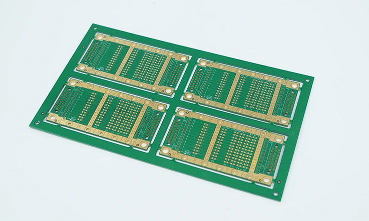
An HDI PCB manufacturer is a company that specializes in producing high-density interconnect printed circuit boards, designed to support the compact and high-speed needs of modern electronics. These manufacturers utilize cutting-edge processes like laser drilling, microvias, and stacked vias to create intricate circuit designs. These boards are designed for high-performance applications, where space is limited but performance must be maximized.
What makes an HDI PCB manufacturer stand out is their ability to handle high-precision tasks that demand specialized knowledge in PCB design and advanced manufacturing processes. The difference between a generic PCB and an HDI PCB lies in the ability to optimize space while maintaining the required signal integrity and performance standards.
For example, consider the shift in the wearable tech industry. Devices like smartwatches or fitness trackers rely on ultra-thin HDI PCBs to ensure that all components fit within the compact body of the device. A PCB manufacturer’s ability to produce these high-density, precise PCBs has a direct impact on the performance, size, and overall usability of these products.
The Role of HDI PCB Manufacturing in High-Tech Industries
HDI PCBs are a fundamental part of high-tech industries that rely on sophisticated electronics. The automotive industry, for example, uses HDI technology in advanced driver-assistance systems (ADAS), where signal integrity and the ability to handle high-speed data transfer are non-negotiable. Similarly, in the medical device industry, HDI PCBs are used in equipment like MRI machines, defibrillators, and wearable health monitors, all of which require precise and reliable circuit designs to ensure accurate performance and patient safety.
For telecommunication companies, HDI PCBs play a central role in the production of 5G infrastructure. These boards are designed to handle high-frequency signals and are used in the small-cell technology that makes up the 5G network.
A case study from a medical equipment manufacturer that utilized HDI PCBs for a new generation of heart monitoring devices highlights how advanced PCBs provide compact solutions while still meeting the rigorous reliability standards required in healthcare. This not only improved device performance but also led to a reduction in manufacturing costs due to the more efficient design enabled by HDI technology.
How HDI PCB Manufacturer Innovations Are Shaping the Future of Electronics?
Innovation in HDI PCB manufacturing continues to push the boundaries of what’s possible in electronics. Human are constantly exploring new ways to integrate flexible PCBs, embedded components, and higher-density layers into their designs. By integrating advanced materials like high-speed laminates and low-loss dielectrics, we can enhance the performance of HDI PCBs, making them even more capable of handling high-speed signals while reducing power consumption.
For instance, the growing use of 3D printing in PCB production allows us to create highly customized and complex multilayered HDI boards more efficiently. This has opened up new possibilities in industries like robotics, where custom PCB shapes and embedded components are needed to meet specific design challenges.
By focusing on automated manufacturing processes and AI-driven design optimization, HDI PCB manufacturers are improving both the speed and precision of their operations. The use of automated inspection systems ensures the highest quality control standards, while AI-driven simulations allow for faster development times and a reduction in production errors.
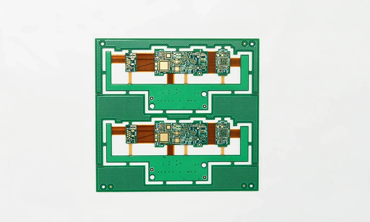
Advanced HDI PCB Stack-Up and Layering Techniques in HDI PCB Manufacturing
The structure of an HDI PCB heavily depends on its stack-up and layering approach, which directly influences how well the final board performs and holds up under real-world conditions. As electronic devices shrink while packing in more functions, configuring the stack-up becomes a tricky puzzle. Knowing the various stack-up designs and their manufacturing effects helps in picking the right setup for any project. This section breaks down different HDI stack-up options and examines how layering impacts signal integrity, routing efficiency, and overall functionality.
Let’s take a closer look at some of the most commonly used stack-up designs, such as 1+N+1, 2+N+2, and any-layer HDI configurations, and examine how each works in various applications.
1+N+1, 2+N+2, and Any-Layer HDI: Which One to Choose?
Choosing between 1+N+1, 2+N+2, and any-layer HDI stack-ups is a process that requires careful consideration of several factors. These include the overall board design, layer count, and the specific electrical requirements of the product.
●1+N+1 Stack-Up: This configuration is composed of a core layer surrounded by one signal layer and one ground plane on each side. It is typically selected for simpler designs that require moderate functionality in terms of routing. Products such as smartphones or consumer electronics often use this design due to the balance it provides between performance and manufacturing efficiency.
●2+N+2 Stack-Up: In this design, there are two signal and ground layers on either side of the core layer. This type of stack-up is typically preferred for products that need more layered complexity and signal integrity, such as automotive electronics or medical devices. It supports more layers without significantly increasing the board thickness, allowing for higher-density designs.
●Any-Layer HDI: Offering maximum flexibility, this configuration allows microvias to be placed in any layer of the board. Any-layer HDI stack-ups are ideal for highly complex designs, such as networking equipment or advanced computing systems, where dense routing and a high number of layers are required.
Tip: A collaborative approach with your HDI PCB manufacturer can help you identify the stack-up that aligns with your project requirements, minimizing complexity while ensuring that performance criteria are met.
Importance of Impedance Control in HDI PCB Manufacturing
In HDI PCB manufacturing, keeping impedance levels steady is a must for reliable high-speed signal transmission. Impedance is the resistance a signal faces as it moves through PCB traces, and factors like stack-up configuration and trace layout can heavily influence it. Getting this balance right ensures signals stay clean and interference-free, preventing performance hiccups in advanced electronic systems.
In high-speed applications like 5G communications, data centers, and high-frequency RF designs, impedance control helps prevent signal degradation, ensuring signal integrity is preserved. During the stack-up process, PCB designers work to control impedance by carefully designing trace widths, adjusting the spacing between layers, and optimizing via placements. Impedance mismatch can result in issues like signal reflection or loss, making it a main part of the design process.
Example: For a medical device that relies on precise data transmission, impedance control ensures that all components within the device operate without interference or signal loss.
High-Density Routing and Fine-Pitch Component Integration
As HDI PCB manufacturers work toward more compact and advanced designs, high-density routing and fine-pitch component integration have become fundamental aspects of modern PCB fabrication. These techniques enable intricate circuits to fit into smaller spaces while maintaining performance and durability. Precision in layout and fabrication ensures that even the most complex boards deliver consistent results in demanding applications.
For example, in a fitness tracker, the compact nature of the design means that several core components like sensors, wireless communication chips, and power management systems need to be placed in a small area. By using fine-pitch components, we can achieve this miniaturization without compromising functionality. Additionally, high-density routing allows for more signal paths to be added to the board without increasing its size.
An example of fine-pitch components could include surface-mount devices (SMD), which are used in products where space constraints are tight. Such components require precise manufacturing techniques, which is why many HDI PCB manufacturers invest in advanced equipment and stringent manufacturing standards.
Example:
Below is a comparison of different routing scenarios:
| Application | Routing Density | Component Size | Stack-Up Type |
| Wearables | High | Fine-pitch | 1+N+1, 2+N+2 |
| Medical Devices | Moderate | Standard | 2+N+2 |
| Networking Equipment | Very High | Fine-pitch | Any-Layer HDI |
This table illustrates the varying routing densities based on the specific needs of the application, highlighting how different stack-ups and routing techniques can be applied.
Key Technologies Used by an HDI PCB Manufacturer
In HDI PCB manufacturing, a variety of advanced technologies are applied to meet the demands of intricate and reliable electronic designs. These technologies enable the production of small-scale, highly-efficient circuit boards that are widely used across industries like consumer electronics, automotive systems, and medical equipment.
In this section, we’ll dive into the key technologies used by HDI PCB manufacturers, covering microvia technology, laser drilling, and sequential lamination. Each of these technologies offers unique advantages for designing and manufacturing HDI PCBs, ensuring that the boards are not only compact but also optimized for high-performance applications.
Microvia Technology: Blind Via, Buried Via, and Via-in-Pad
When discussing HDI PCB design, one of the most efficient methods to achieve dense interconnections is through microvia technology. Microvias, which are small holes drilled into a PCB, allow for making connections between layers in a compact space, which is particularly useful for creating high-density interconnects.
Here are the common types of microvias used in HDI boards:
●Blind Via: This via type links an outer layer to one or more internal layers without passing through the entire board. Blind vias are widely utilized in multilayer HDI PCBs, particularly in compact devices like smartphones and wearable electronics. They help optimize space and enhance routing efficiency, allowing for miniaturization while maintaining circuit functionality.
●Buried Via: Buried vias only connect layers within the board, without reaching the outer surface. This makes them ideal for routing signals between internal layers in designs that require a clean outer layer for additional components. For example, in network equipment or high-performance computing devices, buried vias enable complex routing without adding extra surface area.
●Via-in-Pad: A via-in-pad is located directly in the copper pad where a component would be mounted. This design allows for high-density interconnections in a compact form. While this design is useful for advanced computing systems or automotive electronics, special attention is required during manufacturing to ensure the vias do not cause defects.
Example of Microvia Use:
| Application | Via Type | Purpose | Benefit |
| Smartphones | Blind Via | Connecting outer and inner layers | Saves space and increases design density |
| Network Equipment | Buried Via | Layer interconnection | Maintains clean surface for components |
| High-frequency Circuits | Via-in-Pad | Compact routing and interconnection | Allows high-density routing in tight spaces |
Laser Drilling in HDI PCB Manufacturing: Precision and Efficiency
Laser drilling is a technique that’s often employed in HDI PCB manufacturing due to its precision and efficiency. Unlike traditional mechanical drilling, laser drilling uses focused light to vaporize the material, creating vias with remarkable accuracy.
In the context of HDI PCB manufacturing, laser drilling offers a few key benefits:
●It allows the creation of extremely fine holes, making it well-suited for microvias and fine-pitch routing in compact designs. This is commonly applied in wearables and medical devices, where maximizing space and maintaining signal integrity are top considerations.
●It reduces the wear and tear on tools, as it doesn’t rely on physical drilling, leading to fewer maintenance requirements.
●Laser drilling is also faster than traditional methods, improving the overall production efficiency.
Laser drilling offers high precision, allowing for the creation of HDI PCBs with fine-pitch components required in advanced electronic designs. This technique is often used in high-frequency circuit boards, where precise tolerances are necessary to ensure proper signal transmission. For instance, in telecommunications or advanced consumer electronics, laser drilling ensures that the holes meet strict specifications, supporting the performance of the circuit board.
Sequential Lamination and Its Role in HDI PCB Reliability
Sequential lamination is a process used in HDI PCB manufacturing that involves adding layers to a PCB one at a time. After each layer is applied, it’s drilled and patterned before the next layer is added, allowing for the creation of intricate, high-density designs.
The process of sequential lamination contributes to reliability in several ways:
●It enables precise control over layering, allowing the design to meet the exact requirements for routing and electrical performance.
●The process is especially beneficial for multilayer boards, where the design demands complex routing between layers while maintaining the integrity of the entire structure.
●For industries like medical devices, aerospace, or automotive systems, where the PCB must meet high standards of durability, sequential lamination helps in building a robust PCB structure that can handle demanding applications.
By carefully layering and bonding each section, sequential lamination provides an excellent solution for designing HDI PCBs that are both compact and durable, supporting intricate circuits for high-end applications.
Materials and Substrates for High-Performance HDI PCB Manufacturing
The materials selected for HDI PCB manufacturing define how well a circuit board handles high-speed signals, thermal variations, and mechanical stress. In industries like 5G, aerospace, and high-performance computing, every layer of an HDI PCB must support signal integrity, reliability, and long-term durability.
Understanding the role of low-loss dielectric materials, copper foil types, and resin systems helps HDI PCB manufacturers fine-tune their processes, ensuring compatibility with advanced electronic applications. Let’s dive into what makes these materials stand out and how they contribute to top-tier circuit board performance.
Low-Loss Dielectric Materials for High-Frequency PCBs
In high-frequency applications, dielectric materials impact signal transmission, impedance stability, and power efficiency. Industries like 5G infrastructure, radar systems, and data centers rely on substrates that keep losses at bay, preventing signal degradation at elevated frequencies.
What Defines a Low-Loss Dielectric Material?
Low-loss dielectric materials typically share these properties:
●Minimal dissipation factor (Df) – Helps maintain clean, strong signals over longer distances.
●Stable dielectric constant (Dk) – Keeps impedance predictable across varying conditions.
●High thermal endurance – Prevents expansion and contraction, reducing the risk of layer separation.
Common Low-Loss Materials-
| Material Type | Dielectric Constant (Dk) | Dissipation Factor (Df) | Application |
| Standard FR-4 | 4.2 – 4.8 | 0.02 – 0.03 | Consumer electronics |
| PTFE-Based (Teflon) | 2.1 – 2.5 | 0.0005 – 0.002 | 5G, radar systems |
| Rogers 4000 Series | 3.3 – 3.6 | 0.002 – 0.004 | RF circuits, high-speed data |
| Megtron 6 | 3.4 – 3.7 | 0.002 – 0.004 | Data centers, networking |
Picking the right dielectric material isn’t just about specifications—it’s about balancing cost, process compatibility, and performance requirements.
Copper Foil, Resin Systems, and Their Impact on HDI PCB Manufacturing
Every HDI PCB manufacturer recognizes that copper and resin systems are integral to signal integrity, EMI shielding, and thermal stability. These materials influence how effectively a PCB manages intricate routing and fine-pitch components while maintaining performance.
Types of Copper Foil-
Copper foils used in HDI PCB manufacturing come in different grades, each suited for specific performance needs:
●Electrodeposited Copper (ED) – Economical but has a rough surface, which may impact high-speed performance.
●Rolled-Annealed Copper (RA) – Flexible and smooth, ideal for high-frequency and flex PCBs.
●Ultra-Low Profile (ULP) Copper – Reduces signal loss and enhances reliability in 5G and data applications.
Resin Systems and Their Influence-
Resins act as the glue holding PCB layers together while also affecting heat resistance, mechanical strength, and electrical insulation. Popular choices include:
●Epoxy Resin – The go-to for standard FR-4 boards.
●Polyimide – Excellent for harsh environments like aerospace and automotive.
●Halogen-Free Resin – Meets stringent environmental regulations for medical and 5G electronics.
| Material Type | Primary Benefit | Common Use |
| Electrodeposited Copper (ED) | Low cost, standard PCB processing | General consumer products |
| Rolled-Annealed Copper (RA) | Greater flexibility, smooth surface | Wearable electronics, 5G devices |
| Ultra-Low Profile Copper | Best for high-frequency applications | Data centers, AI computing |
| Epoxy Resin | Cost-effective, reliable bonding | Mass-market electronics |
| Polyimide | Handles extreme temperatures well | Aerospace, automotive |
| Halogen-Free Resin | Meets environmental standards | Medical, high-end telecom |
Selecting the right copper-resin combination ensures an HDI PCB holds up in demanding applications while keeping manufacturing costs in check.
Choosing the Right Material for High-Speed and 5G PCB Applications
As 5G, AI, and ultra-fast computing take over, PCBs must keep up with rising demands for higher frequencies, lower loss, and stronger thermal management. The right material choices directly impact signal clarity, power efficiency, and overall system stability.
Key Factors to Consider in 5G PCB Material Selection-
1.Signal loss reduction – Materials with low Dk and Df (like Rogers RO4000 or Megtron 6) minimize transmission loss.
2.Thermal stability – Substrates with low coefficient of thermal expansion (CTE) prevent warping at high speeds.
3.Manufacturing compatibility – Materials must support laser-drilled vias, stacked microvias, and multi-lamination processes.
Material Recommendations for High-Speed and 5G Applications-
| Use Case | Suggested Material | Performance Benefit |
| 5G Base Stations | PTFE-Based, Rogers 4350B | Handles millimeter-wave frequencies |
| High-Speed Networking | Megtron 6, Isola Tachyon | Enhances signal clarity |
| AI Processing Units | Low-Dk Polyimide | Improves heat dissipation |
| Medical Imaging | Low-Loss FR-4, Rogers 4003 | Reduces power consumption |
As data speeds continue to grow, selecting materials that support high-frequency performance and efficient heat dissipation can have a considerable impact on the overall reliability and durability of the design.
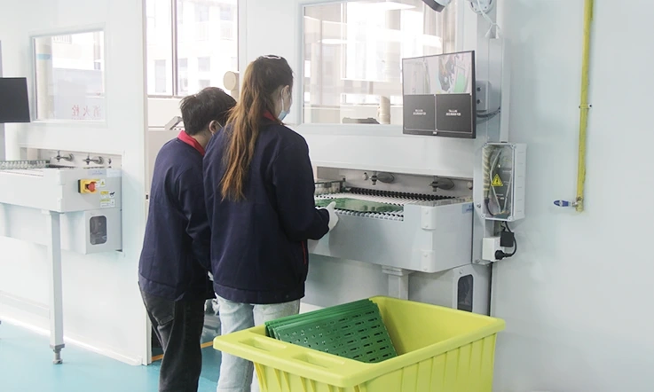
Ensuring Quality and Reliability in HDI PCB Manufacturing
The success of an HDI PCB depends on precision engineering, material integrity, and rigorous validation at every step. With circuits becoming more compact and operating at higher frequencies, HDI PCB manufacturers must implement thorough testing methods to ensure performance remains stable under varying conditions.
From electrical testing and IPC classification to failure prevention strategies, the measures applied throughout production influence a board’s ability to handle high-speed signals, thermal fluctuations, and mechanical stress. Let’s break down the essential steps HDI PCB manufacturers take to keep defects at bay and maintain consistent results.
Electrical Testing and Signal Integrity Verification in HDI PCBs
With the increasing demand for high-frequency and high-density designs, even minor inconsistencies in a PCB can lead to signal degradation or system failure. Thorough electrical testing ensures that microvias, fine-pitch traces, and complex interconnects function as expected.
Flying probe testing is frequently used in prototype and low-volume production, allowing for quick verification of electrical connections without the need for custom fixtures. For high-volume manufacturing, in-circuit testing (ICT) provides more extensive validation by checking component placement, continuity, and resistance.
For high-speed applications such as 5G networks and AI-driven computing, impedance control is an essential consideration. Time-Domain Reflectometry (TDR) testing measures trace impedance consistency, helping PCB manufacturers fine-tune layer stack-ups and routing to prevent signal loss. Meanwhile, Automated Optical Inspection (AOI) is used to detect solder joint defects, misalignment, and surface irregularities before boards move to final assembly.
Skipping proper testing isn’t just a risk—it’s a surefire way to invite signal integrity problems and production headaches.
Reliability Testing Standards: IPC Class 2 vs. IPC Class 3
Different industries have varying requirements for PCB durability, electrical performance, and long-term stability. The IPC classification system provides a benchmark for PCB manufacturers to follow based on application needs.
●IPC Class 2 is typically used in consumer electronics and general applications, where occasional performance fluctuations are acceptable. These boards must meet industry standards for soldering, hole wall integrity, and electrical continuity, but minor imperfections that don’t impact function are tolerated.
●IPC Class 3, on the other hand, is designed for aerospace, medical, military, and automotive electronics, where reliability under extreme conditions is a must. These boards require flawless hole plating, stronger solder joints, and increased resistance to thermal stress. Inspections are far more rigorous, with X-ray analysis, thermal cycling, and burn-in testing included in the validation process.
For applications where failure isn’t an option, IPC Class 3 compliance ensures that a PCB can handle high-temperature environments, vibration, and prolonged operational demands without early degradation. Choosing the right classification is about understanding the end use of the product and ensuring that the PCB is built to last.
Common Failure Modes in HDI PCB Manufacturing and How to Prevent Them
Even with advanced fabrication techniques, HDI PCBs can encounter defects that affect their performance and longevity. Identifying common failure modes and applying corrective measures helps prevent costly rework and ensures that boards perform as expected in their final applications.
●Microvia Cracking – Occurs when vias experience thermal expansion stress. This is often addressed by optimizing laser drilling parameters and ensuring proper plating adhesion.
●Delamination – Results from moisture absorption or poor bonding between layers. Using controlled lamination cycles and low-moisture prepregs reduces the likelihood of this issue.
●Electromigration – A phenomenon where metal atoms shift under high current density, leading to open circuits. Choosing materials with high thermal resistance and maintaining proper trace spacing can prevent this.
●Solder Joint Failures – Arise from mechanical stress, poor reflow profiles, or weak solder paste selection. X-ray inspection and refined soldering techniques help maintain solid joint integrity.
●Impedance Mismatch – Caused by variations in trace width or dielectric properties, leading to signal reflection and data loss. Simulation tools and precise manufacturing control ensure impedance remains within design specifications.
Addressing these potential pitfalls during the manufacturing stage leads to a more reliable final product. Small oversights can quickly turn into large-scale production setbacks if not carefully managed.
Compliance and Certifications Required for an HDI PCB Manufacturer
Manufacturing HDI PCBs isn’t just about stacking layers and etching circuits—it’s about ensuring every board meets strict regulatory requirements. So, whether a PCB is destined for high-speed networking, medical imaging, or automotive control systems, certification guarantees that it performs under real-world conditions without unexpected failures.
From ISO 9001 and RoHS regulations to specialized aerospace and automotive compliance, PCB manufacturers must align with industry benchmarks to stay competitive. Let’s break down the most recognized certifications and what they mean for PCB performance, safety, and global market access.
ISO 9001, RoHS, UL, and Other Regulatory Standards
A well-structured quality system helps an HDI PCB manufacturer keep production consistent, traceable, and aligned with industry expectations. Among the many standards that shape manufacturing, some stand out as non-negotiable for global trade and product reliability:
●ISO 9001 – A foundation for structured operations, covering everything from supply chain management to customer satisfaction tracking.
●RoHS (Restriction of Hazardous Substances) – Governs the use of hazardous materials like lead, mercury, and cadmium in electronic components, making PCBs safer for users and the environment.
●UL (Underwriters Laboratories) Certification – Ensures PCBs meet electrical and fire safety benchmarks, with classifications like UL 94 rating the flame resistance of PCB materials.
●ISO 14001 – Focuses on environmental responsibility, requiring PCB manufacturers to implement waste management, chemical control, and sustainability initiatives.
●IPC-6012 and IPC-A-600 – Define PCB fabrication and inspection criteria, ensuring plating thickness, conductor integrity, and solder mask application meet industry standards.
For HDI PCB manufacturers exporting globally, these certifications aren’t just recommendations—they determine market eligibility. Choosing a supplier with documented compliance helps avoid setbacks like customs delays, recalls, or product rejections.
HDI PCB Manufacturing Requirements for Aerospace and Medical Industries
PCBs used in aerospace and medical fields undergo far more scrutiny than those in commercial electronics. A failure in these applications can mean equipment malfunction, mission failure, or even safety hazards. To prevent such risks, manufacturers must follow strict validation processes and traceability measures.
For aerospace, AS9100 certification builds upon ISO 9001 but extends requirements to include:
●Supply chain control – Ensuring every component, from laminates to copper foils, meets performance expectations.
●Risk management protocols – Addressing material failures, extreme temperature exposure, and radiation resistance for space and aviation electronics.
●Extensive lifecycle testing – Simulating vibrations, pressure changes, and rapid thermal cycling to assess long-term durability.
On the medical side, ISO 13485 governs PCB production for MRI machines, pacemakers, and diagnostic devices. So HDI PCB Manufacturers must meet:
●Biocompatibility requirements – Ensuring materials do not degrade or cause interference in sensitive environments.
●Failure rate monitoring – Tracking and analyzing defect trends to eliminate weak points in production.
●Regulatory approvals – Aligning with FDA (U.S.), MDR (Europe), and other health compliance bodies.
These industries don’t take shortcuts—if a PCB manufacturer wants to supply components for aerospace navigation or life-saving medical devices, compliance is part of the job, not an afterthought.
Automotive and IoT Compliance: Ensuring Quality and Safety
The shift to electric vehicles (EVs), autonomous driving, and IoT connectivity is pushing PCB technology further than ever. Therefore, whether controlling battery management systems, radar sensors, or 5G modules, these boards must withstand constant stress, temperature swings, and electromagnetic interference.
For automotive applications, manufacturers must comply with:
●IATF 16949 – A global standard for automotive PCB quality, focusing on failure prevention, material consistency, and long-term reliability.
●AEC-Q100 & AEC-Q200 – Stress-test components under extreme temperatures, vibrations, and humidity to guarantee durability in high-stress environments.
●ISO 26262 (Functional Safety) – Covers electronics used in braking, steering, and advanced driver-assistance systems (ADAS), ensuring circuits do not introduce performance risks.
Meanwhile, IoT PCBs must meet:
●FCC (Federal Communications Commission) Standards – Regulating wireless transmission, electromagnetic emissions, and interference resistance for smart devices.
●CE Marking (European Compliance) – Required for IoT devices entering the European market, confirming adherence to safety, health, and environmental requirements.
With automotive and IoT products becoming more complex and data-driven, PCB manufacturers must stay ahead of compliance trends. Those who fail to adapt risk being phased out of the supply chain as regulations tighten.
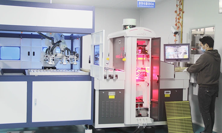
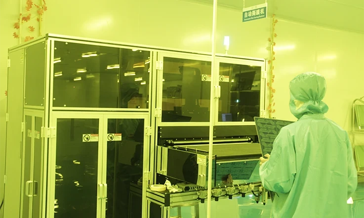
The Role of Automation in HDI PCB Manufacturing
The evolution of HDI PCB manufacturing has brought an increased demand for precision, efficiency, and consistency. Traditional methods that rely heavily on manual operations often struggle to keep up with the complexity of modern PCB designs. With higher circuit density, smaller component pitches, and stringent reliability requirements, automation has become an integral part of advanced HDI PCB production.
From AI-driven quality control to smart factory integration, cutting-edge technologies are redefining how manufacturers optimize workflows, reduce defects, and streamline production. Below, we dive into AI-powered inspection systems, automated optical and X-ray inspection, and the transformation of PCB fabrication through Industry 4.0 smart factories.
AI-Driven Quality Control in HDI PCB Production
As HDI PCBs become more complex, conventional inspection methods struggle to detect micro-level defects. AI-powered quality control systems step in by analyzing solder joints, microvias, and circuit patterns with high precision. These systems learn from real-time production data, allowing HDI PCB manufacturers to adjust process parameters dynamically and eliminate recurring defects before they impact production yield.
Applications of AI in HDI PCB Quality Control-
| AI Technology | Function | Application |
| Pattern Recognition | Detects micro defects | Identifies irregular solder joints, clogged microvias, and etching inconsistencies |
| Predictive Maintenance | Prevents equipment failures | Monitors drilling, etching, and plating processes to prevent malfunctions |
| Real-Time Process Optimization | Adjusts production parameters | Controls etching speed, copper thickness, and drilling accuracy |
By integrating AI, HDI PCB manufacturers can cut down on manual errors, boost first-pass yield, and minimize material waste, leading to more consistent and reliable HDI PCB production.
Automated Optical Inspection (AOI) and X-ray Inspection in HDI PCB Manufacturing
With the growing use of high-density routing and fine-pitch components, traditional manual inspections can no longer keep up. Automated Optical Inspection (AOI) and X-ray Inspection (AXI) provide non-contact, high-speed defect detection, ensuring that even the most intricate PCB layouts are free from production defects.
How AOI Improves PCB Yields-
| AOI Inspection Type | Method | Function |
| Surface Defect Detection | High-resolution cameras | Identifies missing solder pads, circuit breaks, and etching issues |
| Dimensional Accuracy | Laser scanning | Verifies pad dimensions and trace widths |
| Copper Thickness Measurement | 3D imaging | Ensures even etching and plating processes |
Applications of X-ray Inspection in HDI PCB Manufacturing-
| AXI Inspection Type | Function | Suitable for |
| BGA Solder Joint Inspection | Detects hidden defects | Ball Grid Array (BGA), Chip Scale Package (CSP) |
| Microvia Fill Analysis | Evaluates copper plating consistency | Blind and buried vias in HDI PCBs |
| Layer Registration Check | Detects misalignment | HDI stack-ups with 4+N+4 or more layers |
By integrating AOI and AXI, PCB manufacturers can identify defects early, reduce rework rates, and enhance overall product reliability.
Smart Factories and Industry 4.0 in PCB Fabrication
The adoption of smart factory technologies is reshaping PCB manufacturing. By connecting IoT-enabled equipment, real-time data analytics, and automated process control, many PCB manufacturers can optimize production efficiency, minimize human intervention, and maintain consistent quality across high-volume manufacturing.
Core Technologies in Smart Factories-
| Technology | Function | Application |
| IoT-Connected Equipment | Monitors production processes | Tracks drilling, imaging, and plating parameters |
| Adaptive Process Control | Adjusts process settings in real time | Dynamically modifies etching rates and exposure energy |
| Big Data Analytics | Identifies production trends | Predicts defect rates and process bottlenecks |
Traditional vs. Smart Factory PCB Manufacturing-
| Process | Traditional Method | Smart Factory Approach |
| Drilling | Operator sets parameters | Machine auto-adjusts spindle speed and feed rate |
| Etching | Manual monitoring of chemical levels | Sensors adjust chemical composition dynamically |
| AOI Inspection | Human decision-making | AI-driven defect detection for higher accuracy |
With smart factories, HDI PCB manufacturing is shifting toward fully automated, data-driven, and self-optimizing production environments. Manufacturers still relying on outdated manual processes may face challenges in meeting the precision and efficiency demands of industries like 5G, AIoT, and automotive electronics.
How to Choose the Right HDI PCB Manufacturer for Your Business?
Selecting an HDI PCB manufacturer is not just about finding a supplier—it’s about ensuring your products meet the necessary performance, durability, and industry standards. With the increasing complexity of electronic designs, manufacturers must have advanced fabrication techniques, thorough quality control processes, and an efficient supply chain to meet expectations.
Making informed choices regarding supplier selection, budget allocation, and production timelines can prevent unnecessary setbacks and keep projects moving in the right direction. Let’s dive into the details.
Factors to Consider When Selecting an HDI PCB Supplier
A reliable HDI PCB supplier goes beyond offering competitive pricing. The right choice should align with technical expertise, manufacturing capabilities, and compliance with industry regulations. Therefore, if your project involves telecommunications, automotive, aerospace, or consumer electronics, the PCB manufacturer must be able to handle complex builds with precision and consistency.
Several aspects should be examined before making a decision:
●Manufacturing Capabilities: Check for details like minimum line width/spacing, via configurations, and available stack-up options. A supplier with advanced technology can accommodate intricate PCB layouts without production bottlenecks.
●Certifications and Compliance: Ensure your PCB manufacturer follows industry standards like ISO 9001, IPC-6012, UL, and RoHS. These benchmarks help verify that fabrication processes align with recognized quality and safety protocols.
●Equipment and Technology: Facilities equipped with laser drilling, automated optical inspection (AOI), X-ray inspection, and advanced plating methods allow better process control and fewer defects.
●Material Selection: High-performance laminates, copper thickness variations, and low-loss resins directly impact signal integrity and thermal stability. Choosing the right combination can enhance electrical performance without unnecessary cost increases.
●Testing and Inspection Processes: Reliable HDI PCB manufacturers conduct impedance testing, thermal stress analysis, and failure detection to reduce risk and maintain consistency across production batches.
A thorough evaluation of these factors can help you identify a supplier that aligns with your project’s complexity and long-term goals.
Cost vs. Performance: How to Optimize Your PCB Budget?
The cost of HDI PCB production varies based on layer count, via structures, material selection, and panel utilization. Making informed choices in these areas can help control expenses without compromising the end product.
Several factors influence pricing:
●Layer Count: Adding more layers increases costs. Optimizing stack-ups to minimize unnecessary layers can lead to a more efficient design without added expense.
●Via Technology: Buried and stacked vias increase fabrication complexity. When possible, using staggered vias or alternative interconnect methods can streamline manufacturing while maintaining performance.
●Material Choice: High-frequency applications require low-loss materials, but unnecessary over-engineering drives up costs. Selecting materials based on actual electrical and thermal demands ensures a balance between cost and functionality.
●Panel Utilization: Poor layout efficiency leads to material waste. Working closely with the manufacturer to optimize panel usage can improve yield rates and minimize excess costs.
●Testing and Inspection: While additional testing increases production expenses, defining essential verification steps based on application needs helps control spending while maintaining reliability.
Rather than looking for cost-cutting measures that may impact durability, focusing on smart design and production strategies allows for an optimal balance between cost and quality.
Supply Chain Management and Lead Time Considerations in HDI PCB Manufacturing
Efficient supply chain management prevents production bottlenecks, avoids unexpected delays, and keeps projects on track. For HDI PCBs, factors like material availability, production scheduling, and shipping logistics all influence the overall lead time.
Several elements play a role in determining how quickly boards can be delivered:
●Material Procurement: Specialty laminates and copper-clad materials may have extended lead times. Checking availability before finalizing designs helps avoid unexpected delays in production.
●Production Scheduling: High-demand periods can lead to manufacturing backlogs. Working with a supplier that offers flexible scheduling options can help accommodate urgent projects when necessary.
●Testing and Certification: Certain applications require extensive reliability testing, which extends lead times. Planning for these steps in advance ensures the process doesn’t create last-minute hurdles.
●Shipping and Logistics: Customs clearance, transportation delays, and regional disruptions can all impact delivery times. Selecting the right shipping method reduces risk and ensures products arrive when needed.
Why Choose Us as Your HDI PCB Manufacturer?
When it comes to selecting an HDI PCB manufacturer, we offer distinct advantages in terms of technology, quality, service, and delivery times:
1. Advanced Technology
We use microvia technology including blind vias, buried vias, and via-in-pad designs to create high-density, high-performance PCBs. Our high-frequency PCB production employs low-loss dielectric materials and fine-pitch components, meeting the specific needs of industries like 5G, automotive, and medical devices.
| Technology Feature | Description |
| Microvia Types | Blind vias, Buried vias, and Via-in-pad designs for complex HDI PCBs |
| Dielectric Materials | Low-loss dielectric for high-frequency performance |
| Component Density | Fine-pitch component integration for compact designs |
| High-Frequency Capability | Ideal for 5G, automotive, and medical device applications |
2. Consistent Quality
We ensure rigorous electrical testing and signal integrity verification at every stage of the manufacturing process. Our PCBs meet IPC Class 2 and IPC Class 3 standards and comply with global certifications such as ISO 9001, RoHS, and UL, providing products that consistently meet your requirements.
| Quality Metric | Description |
| Electrical Testing | Comprehensive testing for signal integrity and functionality |
| IPC Class Compliance | Meets IPC Class 2 and Class 3 standards for high-reliability applications |
| Certifications | ISO 9001, RoHS, UL certifications ensuring compliance with global standards |
| Signal Integrity | Verification of impedance and signal path for high-speed applications |
3. Personalized Service
Our team works directly with you to understand your project’s unique requirements. We offer expert consultation and support, ensuring that your specific needs are addressed throughout the design and production phases. So, if you are in the medical, aerospace, or automotive industry, we bring specialized knowledge to your project.
| Service Feature | Description |
| Consultation Support | Direct collaboration to tailor designs to your project needs |
| Industry Expertise | Specialized knowledge in medical, aerospace, and automotive sectors |
| Customer Service | Dedicated support throughout the design, production, and delivery process |
| Customization | Ability to handle unique design requirements for a variety of industries |
4. Timely Delivery
We make timely delivery a priority. With a well-organized supply chain and refined production processes, we ensure your HDI PCBs arrive as scheduled, keeping your project on track.
| Delivery Metric | Description |
| Lead Time | Flexible production timelines, tailored to your project schedule |
| Supply Chain Optimization | Streamlined logistics for on-time delivery |
| Production Efficiency | Efficient workflows and processes to ensure timely product completion |
| On-Time Delivery Rate | High percentage of on-time deliveries for customer satisfaction |
Partnering with us means gaining access to advanced technology, reliable quality, attentive service, and flexible delivery times—everything needed to bring your HDI PCB projects to life. Let’s work together to meet your next challenge!


