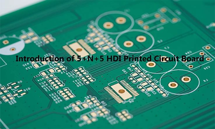
The surging need for compact and high performing electronic devices has led to the development of cutting-edge printed circuit board designs. Among these, the 5+N+5 HDI (High-Density Interconnect) PCB has come to the forefront as a cardinal solution facilitating intricate routing and accommodating numerous components within a compact expanse. This article delves into a profound investigation of the 5+N+5 HDI PCB, its salience in the field of contemporary electronics, and the merits it encapsulates such as circuit density, signal integrity and reliability.
What is HDI Technology Mean?
HDI technology refers to the use of advanced manufacturing techniques and specialized design considerations to create intricate and densely packed circuitry on a PCB.
A paramount characteristic of the HDI PCB is the incorporation of microvias, which are diminutive drilled apertures with diameters usually under 150 micrometers. These microvias facilitate accurate and high density interconnections, allowing the implementation of intricate routing schemes while simultaneously diminishing the size and weight of the PCB.
With their reduced signal length and optimized interconnections, HDI PCB bolster signal integrity, diminish electromagnetic disturbances, and ameliorate comprehensive electrical functionality. They can handle the capacity to accommodate high speed and high frequency signals, thus catering to the spiraling necessity for rapid and proficient data propagation.
What is 5+N+5 HDI PCB?
A 5+N+5 HDI PCB refers to a specific stack up configuration and technology utilized in printed circuit board manufacturing. The term “5+N+5” represents the layer arrangement within the PCB structure.
The “5” in 5+N+5 refers to five signal layers present in the PCB stack up. These signal layers are used for routing electrical signals and components within the circuit board.
“N” symbolizes the quantity of microvia layers incorporated into the PCB. Microvias are smaller drilled holes, typically with diameters less than 150 micrometers, that connect various layers of the circuit board. The particular number of microvia layers can exhibit variation contingent upon design prerequisites and the density of interconnections.
The last “5” signifies five additional signal layer, analogous to the initial quintet of signal layers referred to previously.
Structure of 5+N+5 HDI Printed Circuit Board
A 5+N+5 HDI PCB typically has the following structure:
Core Layer:
The core layer is the central section of the PCB that provides mechanical strength and stability. It’s primarily composed of a non-conductive substance, notably FR-4, which is a fiberglass fortified epoxy laminate typified for PCB creation.
Signal Layers:
In the term “5+N+5”, the “5” corresponds to the count of signal layers inherent in the HDI PCB. Each signal layer houses copper traces and pads, which handle the task of routing electrical signals amongst components. Ordinarily, these layers are typically sandwiched between the core layer and the outer layers.
N Microvia Layers:
The reference to “N” in the term implies the quantity of microvia layers within the HDI PCB. Constituting tiny perforations with diameters rarely superseding 150 micrometers, microvias are instrumental in fostering connections between different signal layers, thus surging the interconnect density. Subject to the design’s requirements, microvias may be either filled with conductive materials or devoid of any plating.
Surface Layers:
The outermost layers of the HDI PCB, often referred to as surface layers or outer layers, provide the interface for the soldering of components and external linkages. These layers, composed of non-conductive substances like FR4, encompass copper traces and pads.
Solder Mask and Legend:
The PCB is typically coated with a solder mask, serving as a safeguard for the copper traces and pads against oxidation and various environmental elements. While the solder mask typically sports a green hue, it can come in other color variations. The legend layer hosts labels and markings, supplying indispensable details like component placement, reference designators and other pertinent data.
Types of 5+N+5 HDI Stack-up
While the precise stack up can fluctuate depending upon the unique requisites of a project, one can categorize the 5+N+5 HDI stack ups under a few common types:
Core-Prepreg-Stacked Microvias-Prepreg-Core (C-P-S-P-C):
This stack up consists of a core layer at the center, followed by layers of prepreg on both sides. Stacked microvias are created between the prepreg layers to establish interconnections. Another core layer is added on the outermost sides. This stack up is often used when there is a need for controlled impedance and dense routing.
Core-Prepreg-Stacked Microvias-Prepreg-Stacked Microvias-Prepreg-Core (C-P-S-P-S-P-C):
In this stack up, an addition of two layers of stacked microvias is made amid the prepreg layers. This provision affords a lift in circuit density and complex interconnet. The stacked microvias yield extra channels for the traces, fostering the accommodation of an increased count of components within a restrained space.
Core-Prepreg-Stacked Microvias-Prepreg-Via-in-Pad-Prepreg-Core (C-P-S-P-VIP-P-C):
This stack-up used via-in-pad (VIP) technology, where vias find placement straight within the component pads. The VIP form a direct nexus from the contact pad of the component to the inner layers, thus decreasing the count of signal layers necessitated. This stack-up proves advantageous in designs with high requirements for component density and signal integrity.
Core-Prepreg-Stacked Microvias-Prepreg-Buried Vias-Prepreg-Core (C-P-S-P-B-P-C):
This stack up includes buried vias, vias which are fully ensconced within the structure of the PCB. Buried vias provide additional routing channels without affecting the outer layer space. Such stack ups garner favor when the demand for amplified layer tally couples with the aspiration to preserve a compact form factor.
These are just a few examples of the stack-up configurations for 5+N+5 HDI PCB. The stack up election is contingent upon explicit design requisites such as signal integrity, impedance control, thermal management and manufacturing feasibility. It becomes imperative to forge a close collaboration with PCB designers and manufacturers to ascertain the most appropriate stack-up configuration apropos a specific undertaking.
How to Design a 5+N+5 A HDI PCB?
The execution of a 5+N+5 HDI PCB design demands meticulous strategizing and adherence to certain design norms.
Determine Requirements:
Clearly define the requirements of your PCB, including size constraints, electrical performance needs, and interconnect density goals. Identify the number of signal layers (5), the number of microvia layers (N), and the desired thickness of each layer.
Work with an Experienced Designer:
Consider forging synergy with a seasoned PCB designer proficient in HDI technology. Harnessing their expertise will enable you to translate your requisites into an efficient design that ensures optimal space utilization, impeccable signal integrity and seamless manufacturability.
Layer Stack up:
Develop a layer stack-up that accommodates the necessary signal, core, and microvia layers. Consider the thickness and type of materials to be used, such as FR4 or high frequency laminates, and ensure proper impedance control between layers.
Component Placement:
Carefully place components on the PCB to optimize signal routing, minimize trace lengths, and consider thermal considerations. Use the available space efficiently, making use of high density component packages and placing critical components strategically.
Microvia Planning:
Determine the required microvia structures to achieve the desired interconnect density. Evaluate the use of blind vias, buried vias, and stacked vias based on the layer stack-up and component placement. Ensure proper clearance and alignment between microvias and adjacent pads/traces.
Routing Considerations:
Plan the routing of the PCB traces, paying attention to impedance control, signal integrity, and EMI (Electromagnetic Interference) mitigation. Utilize differential pairs, controlled impedance routing, and proper ground/signal plane placement to minimize signal distortions.
Design for Manufacturing (DFM):
Consider design rules and guidelines provided by your PCB manufacturer during the design process. Ensure that your design can be manufactured using the available manufacturing processes. Like laser drilling and sequential lamination.
Design Verification:
Perform thorough design verification using simulation tools, signal integrity analysis, and design rule checks. Verify that the design meets the desired electrical performance criteria and manufacturability requirements.
Design Iteration and Collaboration:
Iterate on the design based on feedback from manufacturing partners and design reviews. Collaborate closely with your PCB manufacturer to address any design optimizations or manufacturing challenges.
How to Choose the Right PCB laminate for 5+N+5 HDI Designs?
The selection process for the PCB laminate material in a 5+N+5 HDI PCB design involves contemplating several crucial factors.
Electrical Performance:
Evaluate the electrical attributes of the laminate, encompassing dielectric constant and loss tangent. These particular properties govern signal integrity, impedance control and high frequency performance. Confirm that your chosen laminate meets the specified electrical performance for your design.
Material Thickness:
Consider the thickness options available for the laminate. The thickness of the material directly influences the overall PCB thickness and stack up arrangement. Ensure that the options offered for laminate thickness align harmoniously with your design requisites and limitations.
TG (Glass Transition Temperature):
Evaluate the TG, or glass transition temperature, of the laminate. This value represents the temperature threshold at which the substance shifts from a rigid state to a more flexible one. Choose for a laminate with a TG that aligns with your intended operational temperature domain to guarantee the PCB’s structural and thermal stability
CTE (Coefficient of Thermal Expansion):
Consider the CTE of the laminate material. CTE mismatch between different layers can cause reliability issues such as thermal stress and delamination. Ensure that the chosen laminate has a compatible CTE with other layers in the stack-up to minimize reliability concerns.
Material Compatibility:
Verify the compatibility of the laminate with microvia production processes. Certain laminate materials might demonstrate compatibility problems with laser drilling and sequential lamination utilized in HDI designs. Guarantee that the selected laminate is apt for the microvia construction techniques applied in your 5+N+5 HDI design.
Manufacturing Support:
Collaborate with your chosen PCB manufacturer to ensure they have experience working with the selected laminate. Confirm their capacity to successfully process and fabricate the laminate with their equipment and processes. The manufacturer’s acquaintance with the chosen laminate will substantially influence the achievement and feasibility of your 5+N+5 HDI design.
Reliability and Quality:
Take into account the reputation of the laminate manufacturer in yielding high grade and reliable materials. Look for certifications and adherence to industry standards to ensure that the laminate’s compliance with necessary reliability specifications.
Cost Considerations:
Evaluate the cost effectiveness of the laminate. Balancing the desired performance and features with the project budget is essential. Compare prices from different manufacturers and request quotes to select a laminate that fits within your budget while meeting your requirements.
Why You Need 5+N+5 HDI PCB Board?
In some cases using 5+N+5 HDI PCB board can offer advantages. Below are a reasons why you might find a 5+N+5 HDI PCB board necessary:
High component density: The 5+N+5 layout facilitates an elevated component density on the board, advantageous in applications where space is constrained. This permits an increase in functionalities, promoting the miniaturization of electronic devices.
Better signal integrity: HDI PCB board generally possess a diminished number of signal layers, lessening the distance and impedance amid components. This leads to better signal integrity, decreased cross talk and a reduction in electromagnetic interference.
Enhanced electrical performance: The design of HDI PCB aids in enhancing electric performance by curtailing transmission line lengths, diminishing signal losses and ameliorating signal quality. This factor is especially pivotal for applications of high speed and high frequency nature.
Increased reliability: The use of HDI technology allows for shorter and more direct interconnections, reducing the risk of signal distortion and potential reliability issues. It also promotes the application of fine pitch constituents and smaller via dimensions, augmenting the overall reliability of the PCB.
Cost effectiveness: While the introductory production expenses of HDI PCB may seem steep due to their intricate nature, they could yield substantial cost reductions over time. The reduced board size, lighter weight, and optimized performance can result in lower material and assembly costs, improved product functionality, and potentially reduced energy consumption.
Key Considerations for Manufacturing 5-N-5 HDI Circuit Boards
Manufacturing 5+N+5 HDI circuit boards requires careful attention to various considerations to ensure successful production. Here are some key factors to consider:
Design and Layout:
The schematic design and layout of the PCB hold paramount importance in its production. Collaborating closely with seasoned PCB designers who hold proficiency in HDI technology remains essential. The designed layout must focus on optimizing signal routing, minimize impedance mismatches, and consider the placement of microvias and components.
Material Selection:
Selecting the correct pcb base materials is paramount for attaining the intended functionality of the HDI PCB. Evaluate the foundational substance, such as FR4 or high frequency laminates, and go for materials having suitable dielectric constants, thermal properties and size stability.
Manufacturing Processes:
HDI PCB often require specialized manufacturing processes. It’s critical to ascertain that your PCB manufacturer possesses the requisite skills and expertise to manage the involved fabrication methodologies. Such as laser drilling, sequential lamination, the creation of microvias and copper plating.
Microvias:
Microvias are a central feature of HDI PCB. Determine the optimal via size, aspect ratio, and pad design based on your specific requirements. Consider whether blind vias, buried vias, or stacked vias are necessary to achieve the desired interconnect density.
Copper Plating:
Achieving reliable copper plating in the microvia structures is crucial for maintaining good electrical performance. It is important to select appropriate plating processes and ensure uniform and void-free copper deposition to minimize signal losses.
Quality Control:
Enact rigorous quality control measure throughout each manifold of the manufacturing process. This involves exhaustive scrutiny, testing protocols, and validation procedures to verify that the ultimate product conforms to the requisite specifications and reliability standards.
Collaboration with PCB Manufacturer:
Effective communication and collaboration with your PCB manufacturer are essential for successful HDI PCB manufacturing. Engage in early discussions to review the design, discuss fabrication capabilities, clarify requirements, and address any technical concerns.
Which Industries Benefit from 5+N+5 HDI PCB?
Telecommunications:
The telecommunications sector leans heavily on high speed data conveyance, miniaturization and increased functionality. HDI PCB can accommodate the complex interconnections required by devices such as smartphones, 5G base stations, routers and networking equipment.
Consumer Electronics:
Consumer electronics, including portable devices, wearable technology, gaming systems and smart home. These products apparatus can benefit from the compact size and improved electrical performance offered by HDI PCB. These boards facilitate the integration of multiple features within the confines of restricted space.
Automotive:
The automobile sector exhibits an amplified dependence on electronic systems for aspects such as navigation, infotainment, connectivity, driver support and security. HDI PCB can uphold the elevated density packaging mandated for these systems, thereby optimizing spatial utility and endorsing reliable performance under strenuous automotive conditions.
Medical Devices:
Medical devices often require compact designs and high functionality to meet the demands of patient monitoring, diagnostics, imaging, and treatment systems. HDI PCB enable the miniaturization of medical devices while maintaining reliable and precise electrical connections.
Aerospace and Defense:
The aerospace and defense sectors require PCB that can withstand extreme conditions, maintain signal integrity, and accommodate intricate interconnections. HDI PCB can meet these requirements while reducing weight and size in avionics systems, satellites, military equipment, and communication devices.
Industrial Automation:
Industrial automation systems, including robotics, control systems, and sensors, benefit from HDI PCBs‘ ability to handle complex interconnections, deliver high-speed signal transmission, and maintain consistent performance in demanding industrial environments.
In a Word
The rise of 5+N+5 HDI PCB technology has transformed the landscape of electronic circuitry by providing unprecedented advantages to various industries. The capacity to attain a loftier component density, progressive miniaturization, superior electrical efficacy, and bolstered dependability has fueled the broad-based assimilation of 5+N+5 HDI PCB technology.
As the demand for smaller and more powerful electronic devices continues to soar, the importance of 5+N+5 HDI PCB becomes increasingly critical. Demonstrating shown immense versatility and potential, this types PCB facilitate the progression of superior telecommunication infrastructures and the performance of entities such as consumer electronics, medical appliances, automotive systems and aerospace applications.
Persistent progress in fabrication processes and design techniques will only augment the advantages and utilities of 5+N+5 HDI PCB in prospective times. With technological evolution, it becomes essential to remain at the vanguard of these advancements, harnessing the potentialities conferred by 5+N+5 HDI PCB to spur innovation and accommodate the morphing requisites of the electronics sector.

