
As electronic devices grow in capability while the space for their internal components shrinks, engineers naturally turn their attention to High-Density Interconnect (HDI) technology. Among the many HDI structures, the 4+N+4 architecture stands out for its refined balance of routing density, signal integrity, and design freedom.
This guide will accompany you on the complete journey of a 4+N+4 HDI board. We will not only explore the essence of its design philosophy—from stackup architecture and material selection to the intricate manufacturing and assembly processes that bring it to life—but we will also engage in a practical discussion of business considerations, including quality assurance protocols, cost drivers, lead time planning, and its real-world application stories.
Decoding the Art of the 4+N+4 Stackup
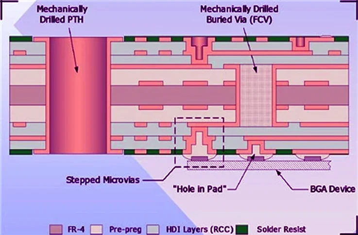
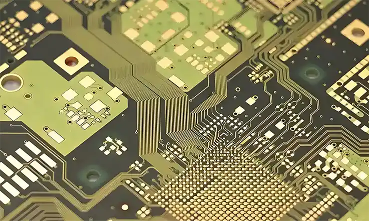
When an electronic device must integrate more functionality within a smaller footprint, the printed circuit board (PCB) beneath it must evolve in kind. The 4+N+4 High-Density Interconnect (HDI) stackup is an advanced PCB architecture born from this challenge. It features a central core (the ‘N’ layers) with four sequentially laminated HDI layers on both its top and bottom. This construction unlocks immense routing potential for sophisticated electronics, allowing them to perform reliably under demanding space and signal integrity requirements.
By employing technologies like laser-drilled microvias, stacked vias, and via-in-pad designs, the 4+N+4 structure creates exceptionally short and direct pathways between layers. This approach is fundamental to achieving compact layouts and optimizing high-speed data transmission without expanding the board’s physical footprint.
1.Defining Features of the 4+N+4 Architecture
The term “4+N+4” vividly describes the board’s physical construction. This multi-stage lamination process yields a highly integrated board with distinct characteristics:
●Exceptional Routing Density: This structure allows for finer lines and spaces, enabling designers to place more electrical pathways and components within a confined area.
●Flexible Interconnect Design: It supports complex interconnect schemes, such as stacking microvias on top of each other. This provides direct, efficient connections between non-adjacent layers.
●Enhanced Signal Performance: Shorter signal paths reduce signal degradation, delay, and crosstalk, which benefits high-frequency and high-speed digital applications.
●Support for Miniaturization: These features collectively allow for the creation of smaller, lighter, and more powerful electronic products.
2.How 4+N+4 Compares to Other HDI Structures?
The “x+N+x” naming convention is a simple way to classify the complexity of an HDI board. As ‘x’ increases, so does the routing capability and manufacturing intricacy.
| HDI Stackup Type | Typical Number of HDI Layers per Side | Typical Minimum Line/Space (µm) | Suitable Application Examples |
| 1+N+1 | 1 | 50 – 75 | Moderate routing: IoT devices, basic consumer electronics |
| 2+N+2 | 2 | 40 – 60 | Mid-level density: Wearables, automotive modules |
| 4+N+4 | 4 | 25 – 40 | High-density: Premium smartphones, medical devices, aerospace systems |
●1+N+1 & 2+N+2: These are foundational HDI structures suitable for designs with moderate routing requirements. They introduce the benefits of microvias but have fewer layers for complex interconnects.
●4+N+4: This structure represents a significant step up in density. By providing four HDI layers on each side, it opens up an extensive range of routing options not possible with simpler stackups, striking a fine balance between high performance and manufacturability.
Design and Layout Considerations for 4+N+4 HDI PCBs
A successful 4+N+4 HDI design is a matter of balancing ambitious density goals with the practical limits of fabrication. It requires a deep understanding of microvia structures, trace routing capabilities, and the philosophy of Design for Manufacturing (DFM). These guidelines will help you navigate the decisions in these areas to engineer a board that is both high-performing and manufacturable at scale.
Interconnect Structures: The Science of Vias
Vias create the vertical electrical connections that form the backbone of a 4+N+4 stackup. Your choice of via type and arrangement directly impacts board density, signal integrity, and overall reliability.
1.Fundamental Via Types:
●Blind Vias: Connect an outer layer to an inner layer, ideal for routing signals directly from surface-mount components into the board.
●Buried Vias: Connect only internal layers. They are invisible from the outside, maximizing the available space on the top and bottom surfaces for component placement.
2.Microvia Arrangements:
●Stacked Microvias: Aligned vertically across multiple layers to create a direct, pillar-like connection. This offers the shortest possible signal path and maximizes routing channels, though it demands very precise manufacturing control.
●Staggered Microvias: Offset from layer to layer. This configuration often enhances reliability under thermal stress and can be a more forgiving structure during fabrication.
Surface Layout: Traces and Pads
The top-level details of your layout are where density and signal performance are ultimately realized.
| Layout Parameter | Typical Values | Impact on Performance |
| Trace Width | 50 µm or finer | Controls impedance, reduces crosstalk |
| Trace Spacing | 50 µm or finer | Prevents shorts, controls coupling |
| Via-in-Pad Diameter | 100 – 150 µm | Saves PCB real estate, shortens signal path |
| Annular Ring (Via) | ≥ 75 µm | Ensures mechanical and electrical reliability |
●Trace Width and Spacing: While the goal is often to use the narrowest traces possible, these must remain well within your fabricator’s capabilities (e.g., modern processes can often achieve trace/space dimensions of 50µm/50µm or less). Controlling these dimensions precisely is fundamental for managing impedance and minimizing signal crosstalk on high-speed lines.
●Via-in-Pad Technique: Placing a microvia directly within a component’s solder pad is a powerful technique for saving space and shortening signal paths. To be successful, this method requires the via to be completely filled and plated over (capped) to create a perfectly flat surface. This planarity is a decisive factor in preventing soldering defects during the assembly stage.
Manufacturing-Aware Design (DFM) and CAD Setup
Integrating DFM principles from day one is the most effective strategy for ensuring a smooth path from design to production. This approach means treating your manufacturer’s capabilities as part of the design specification.
●Collaborate Early and Often: Don’t wait until the design is “finished.” Engage with your PCB supplier early in the process. This allows their engineers to provide valuable feedback on your stackup, material choices, and feature sizes, helping you avoid costly and time-consuming revisions.
●Configure CAD Rules Precisely: Set your CAD tool’s design rules to the specific, real-world values of your chosen manufacturer, not to generic industry minimums. This includes their exact tolerances for trace width, spacing, annular rings, and via drilling.
●Adopt a Holistic DFM/DFMA Approach: True DFM considers not only fabrication but also assembly (Design for Manufacturing and Assembly). This is especially relevant for HDI. A layout feature like via-in-pad, if not perfectly executed in fabrication, can cause significant soldering issues during assembly.
Working with a partner (JarnisTech) that provides both PCB fabrication and assembly services offers a distinct advantage. We can provide integrated DFM/DFMA feedback that optimizes the entire process, ensuring your design is not only buildable but also robustly assembled for long-term reliability.
Material Selection for 4+N+4 HDI PCBs
The choice of materials is a foundational decision in the design of a 4+N+4 HDI board, directly influencing its electrical performance, thermal behavior, and ability to endure the multi-stage lamination process. A careful combination of dielectric substrates, copper foils, and laminates ensures the final product meets its performance targets for signal integrity and long-term reliability. This section explores the material characteristics that affect the function and manufacturability of these advanced boards.
Dielectric Materials and Signal Integrity
For high-frequency and high-speed applications, the dielectric material’s properties are a primary focus. The objective is to select materials with stable electrical characteristics across a range of operating conditions. Commonly specified material families for these applications include series from Rogers, Isola, or Panasonic, though the ideal choice is always application-dependent.
●Dielectric Constant (Dk): A material’s Dk affects signal speed and impedance control. Materials with a low, stable Dk are preferred as they allow for faster signal propagation and make it easier to maintain tight impedance tolerances.
●Dissipation Factor (Df): Also known as loss tangent, Df measures how much signal energy is absorbed and lost as heat within the dielectric. Low-Df materials are selected for high-frequency circuits to minimize signal attenuation.
●Thermal Conductivity: Materials with higher thermal conductivity help dissipate heat away from active components like processors, contributing to the overall thermal stability of the device.
●CAF Resistance: In dense HDI layouts, resistance to Conductive Anodic Filament (CAF) formation is a notable reliability consideration. CAF is an electrochemical migration process that can cause shorts between conductors. Selecting materials with proven CAF resistance is a safeguard in designs with tight spacing.
Build-Up Materials: Cores, Prepregs, and Copper Foils
The physical construction of a 4+N+4 stackup relies on the synergy between its core, bonding layers, and conductive foils.
| Material Type | Typical Thickness | Key Properties | Design Considerations |
| Core | 0.2 mm – 1.6 mm | Rigid dielectric with copper cladding | Must match prepreg resin system to avoid warping |
| Prepreg | 30 – 150 µm | Resin-impregnated fiberglass cloth | Provides bonding, must have compatible CTE (Coefficient of Thermal Expansion) |
| Copper Foil | 9 – 35 µm (0.25 – 1 oz) | Conductive, supports fine trace etching | Thinner foils enable finer features but lower current capacity |
1.Cores and Prepregs:
A core is a rigid piece of dielectric with copper foil on both sides, forming the central foundation (the ‘N’ layer). Prepregs are fiberglass cloths pre-impregnated with resin that act as a bonding agent to laminate additional layers onto the core during the sequential build-up process. Matching their properties is needed to ensure a uniform, warp-free final board.
2.Copper Foil:
The thickness and type of copper foil determine the board’s current-carrying capacity and its ability to support fine-line features. Thinner foils allow for more precise etching of narrow traces required in HDI designs, but the selection must be balanced with the signal’s power requirements.
Surface Finishes for Solderability and Protection
The surface finish is the final coating applied to the copper pads, protecting the surface from oxidation and providing a solderable surface for component assembly. This choice has direct implications for the assembly process and overall product reliability.
●ENIG (Electroless Nickel Immersion Gold): Offers a very flat surface and excellent solderability, making it well-suited for fine-pitch BGAs and other sensitive components. It is a widely used and highly reliable finish.
●OSP (Organic Solderability Preservative): A cost-effective and environmentally friendly option that provides a flat surface. However, OSP has a limited shelf life and can degrade after multiple thermal cycles. Its short process window makes it an ideal candidate for projects where a fast, streamlined workflow from fabrication to assembly is managed by a single partner.
●ENEPIG (Electroless Nickel Electroless Palladium Immersion Gold): Often called the “universal finish,” ENEPIG offers superior reliability for both soldering and gold wire bonding. Its robustness and durability make it suitable for the most demanding applications, although it is typically the premium-priced option.
The Manufacturing Journey of a 4+N+4 Board
Producing a 4+N+4 HDI PCB is a meticulous, multi-stage operation where precision at every step dictates the final product’s quality and performance. The process is defined by a sequential layering method that builds the board’s complex structure from the inside out. Understanding this workflow is helpful for designers looking to optimize their layouts for manufacturability.
Data Preparation and Inner Layer Creation
Before any physical work begins, the design data must be prepared and the board’s foundation created.
●Computer-Aided Manufacturing (CAM): In this initial stage, your design files are translated into detailed machine instructions. CAM engineers verify the data against manufacturing rules and panelize the layout to optimize production efficiency, preventing costly errors before fabrication starts.
●Inner Layer Imaging and AOI: The circuit patterns for the innermost core (the ‘N’ layer) are imaged onto copper-clad laminate. After this pattern is etched, these foundational layers undergo Automated Optical Inspection (AOI) to detect any defects like shorts or opens. This quality check is fundamental, as these layers will be inaccessible once the board is built up.
The Sequential Build-Up Cycle
The defining characteristic of 4+N+4 manufacturing is the repetition of a lamination cycle to add the four HDI layers to each side of the core. This cycle, repeated eight times in total, includes:
●Laser Drilling: High-precision lasers (typically using CO2 lasers for dielectrics and UV lasers for finer features) create the microscopic blind vias that connect one layer to the next. The accuracy of the laser’s position and depth is a basic requirement.
●Via Formation and Plating: The newly drilled microvias are cleaned and then made conductive through a multi-step copper plating process. This creates a reliable electrical connection through the via.
●Lamination and Bonding: A new layer of dielectric material (prepreg) and copper foil is bonded to the existing structure using carefully controlled heat and pressure.
●Registration: With each new layer added, maintaining perfect alignment (registration) to the layers below becomes progressively more challenging. Achieving precise registration across all build-up cycles is a hallmark of a capable HDI manufacturer.
Outer Layer Patterning and Final Quality Assurance
Once all layers are built up, the board enters the final production stages.
●Outer Layer Patterning: The external circuit patterns, including component pads and traces, are imaged and etched onto the outer copper layers. This requires high precision to accommodate the fine-pitch components that are common in HDI designs.
●Final Inspection and Electrical Test: After the surface finish is applied, every board undergoes a final visual inspection and a comprehensive electrical test, often using flying probe or bed-of-nails testers. This test verifies that all connections are intact and match the original design netlist, confirming the board’s integrity.
| Final Step | Activity | Parameters / Methods | Quality Outcome |
| Outer Layer Patterning | Imaging and etching of outer layers | Line width: 30–50 µm; Etching precision | Supports fine-pitch components |
| Final Inspection | Visual and automated inspection | Tools: AOI, X-ray, flying probe | Detects surface defects and open/short circuits |
| Electrical Test | Continuity and isolation testing | Test voltage: 100–200 V; Test time: ~10 s per board | Confirms board electrical integrity |
A board that successfully passes this rigorous testing is confirmed to be a high-quality bare board, ready for the next critical stage: component assembly.
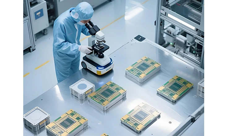
Assembling High-Density Boards: A Discipline of Precision
The assembly of a 4+N+4 HDI board is a discipline of precision. The board’s dense and intricate structure moves beyond standard assembly processes, demanding advanced equipment, materials, and process control. Successfully assembling these boards requires a deep understanding of how to handle ultra-fine-pitch components, manage complex thermal profiles, and address the unique challenges presented by HDI fabrication techniques. This section outlines the solutions required for high-yield, high-reliability HDI assembly.
Handling High-Density and Fine-Pitch Components
The use of modern packages like µBGAs, QFNs, and CSPs with pitches of 0.4mm or less leaves no margin for error. Success depends on mastering several factors:
●Precise Pad and Mask Control: Assembly of fine-pitch devices requires flawless solder mask registration and uniform pad sizes. Non-Solder Mask Defined (NSMD) pads are often specified for BGAs to allow the solder ball to wet around the sides of the pad, creating a stronger, more easily inspected joint.
●Component Placement Accuracy: High-precision pick-and-place machines with advanced vision systems are needed to accurately position components onto tiny land patterns, especially on via-in-pad structures where the available surface area is limited.
●Mechanical Robustness: For devices subjected to physical stress, such as those in mobile, automotive, or aerospace applications, underfill processes are often applied after reflow to mechanically reinforce the thousands of delicate solder joints, dramatically improving long-term reliability.
Precision Soldering and Thermal Management
The dense layout and multiple layers of a 4+N+4 board create a complex thermal landscape that must be carefully managed during reflow soldering.
●Customized Reflow Profiles: A generic thermal profile is guaranteed to cause defects. Proper profiles must be developed using multiple thermocouples on the actual board to account for thermal mass variations and prevent issues like head-in-pillow, cold joints, or solder beading.
●Solder Paste and Volume Control: Controlling the precise volume of solder paste deposited is a point of focus. For via-in-pad designs, this prevents solder from wicking down into the via and ensures a sufficient amount remains on the pad to form a reliable joint with the component.
●Advanced Inspection: After assembly, advanced inspection is non-negotiable. 3D Automated Optical Inspection (AOI) verifies component placement and the quality of every solder joint. For components like BGAs, 2D or 3D X-ray inspection is used to see through the package and confirm there are no hidden defects like shorts or voids.
Stencil Design and Surface Preparation
The success of the entire soldering process begins with a perfect foundation: the solder paste deposit and the board surface itself.
●Advanced Stencil Technology: For fine-pitch components, standard stencils often fall short. High-performance stencils—typically laser-cut with electropolished apertures and proprietary nano-coatings—are employed to promote clean paste release and reliable deposition across even the smallest pads.
●The Prerequisite of Planarity: The via-in-pad technique, which is indispensable for HDI routing, requires the via to be filled and plated over to create a perfectly flat—or planar—surface. This step occurs during fabrication, but its quality has the single greatest impact on assembly yield. A non-planar surface will lead to poor gasketing during solder paste printing, resulting in inconsistent solder deposits, tilted components, and faulty joints.
| Process Element | Specification / Practice | Purpose |
| Stencil Type | Laser-cut + electropolished | Ensures clean paste release |
| Aperture Design | Optimized for 0.4 mm pitch or finer | Prevents bridging or insufficient solder |
| Nano-Coating | Fluoropolymer-based or similar | Reduces paste adhesion inside apertures |
| Surface Planarity | ≤15 µm across local pads | Enables uniform solder paste printing |
This direct and unbreakable link between a fabrication outcome and an assembly result makes a compelling case for a unified manufacturing approach.
Ensuring Quality: Verification from Start to Finish
For complex 4+N+4 HDI boards, quality assurance is an integrated discipline that extends from initial data verification to final inspection. The density of these designs requires a multi-faceted testing strategy to verify every aspect of the board, from the integrity of internal microvias to the robustness of the final build. These verification checkpoints ensure conformance with design specifications, stack-up tolerances, and international standards.
In-Process Inspection and Verification
These non-destructive methods are used throughout the production line to monitor quality and catch potential defects early, when they are easiest to correct.
●Automated Optical Inspection (AOI): After each layer is etched, high-resolution AOI systems scan the copper patterns to find defects like trace shorts, opens, or incorrect spacing—which is particularly useful for fine-line HDI features that are too small for human inspection.
●X-Ray Inspection: X-ray provides a unique view inside the board. It is used to verify the alignment of internal layers and, most importantly, to analyze the registration of stacked microvia structures, ensuring one via is perfectly centered over the one below it.
●Flying Probe Testing: Before a board is released for assembly, this fixtureless electrical test checks every net on the bare board for continuity and isolation. It is the final gatekeeper that confirms the board’s electrical circuitry perfectly matches the original design data.
Process Validation and Reliability Testing
These tests, typically performed on representative test coupons from each production panel, are used to validate the manufacturing process itself and ensure long-term reliability.
●Micro-sectioning (Cross-Section Analysis): A physical cross-section of the board is cut, polished, and examined under a high-magnification microscope. This provides direct visual evidence of plating thickness inside vias, the quality of layer-to-layer lamination, and the structural integrity of stacked microvias.
●Thermal Cycling: Boards are subjected to hundreds or even thousands of rapid temperature cycles (e.g., from -40°C to 125°C). This accelerated life test is designed to expose any latent weaknesses in the structure, such as via barrel fatigue or potential for delamination.
●Peel Strength Testing: This destructive test measures the force required to peel a copper trace from the dielectric substrate. It validates the bond strength between the materials, ensuring the board will withstand the thermal and mechanical stresses of assembly and real-world operation.
●TDR Testing (Impedance Control): For high-speed designs, Time Domain Reflectometry (TDR) is used to send a signal through designated traces to verify they meet their specified impedance value (e.g., 50Ω single-ended or 100Ω differential). This is a requirement for maintaining signal integrity.
Adherence to IPC Class 2 vs. Class 3 Standards
IPC standards provide a universal benchmark for quality and acceptance criteria. The choice of classification is one of the most consequential decisions for a project.
●IPC Class 2: This is the standard for most general commercial and consumer electronics. It represents a robust and reliable product, with specifications that balance performance and cost-efficiency.
●IPC Class 3: This is the highest reliability standard, reserved for applications where failure is not an option, such as in aerospace, defense, and medical life-support systems. Class 3 imposes much stricter tolerances on all aspects of production, from tighter annular ring requirements to zero tolerance for certain voids in via fills.
| Feature / Requirement | IPC Class 2 | IPC Class 3 |
| Annular Ring Tolerance | ≥50 µm | ≥75 µm |
| Via Fill Quality | Voids allowed within limits | Void-free mandatory for filled vias |
| Electrical Test Requirement | 100% of boards (bare net test) | 100% of boards + higher test voltage |
| Inspection Criteria | Cosmetic defects permissible if functional | Stricter—cosmetics may indicate weakness |
| Application Examples | Consumer electronics, commercial products | Medical, military, aerospace |
The decision between Class 2 and Class 3 is a foundational one that affects design rules, material selection, manufacturing processes, testing protocols, and ultimately, cost.
Production Planning: Timelines, Yield, and Scale
Successfully bringing a 4+N+4 HDI product to market requires more than technical fabrication; it demands robust production planning. The intricate nature of these boards necessitates a collaborative approach to scheduling, yield management, and scaling. A transparent understanding of the entire production lifecycle is the foundation for meeting deadlines and achieving cost targets at volume.
Prototype vs. Mass Production Timelines
The timeframe for 4+N+4 HDI boards differs significantly between the initial prototype phase and full-scale production.
●Prototyping: This stage involves considerable front-end engineering, including DFM validation, custom tooling creation, and impedance modeling. The multiple lamination cycles and complex via processing inherent to HDI result in a longer prototype lead time compared to standard PCBs. This initial investment in time is a deliberate measure to ensure a stable and high-yield process for future runs.
●Mass Production: Once the design is validated and the process is locked in—often through a small-scale pilot run—production shifts to a focus on repeatability and efficiency. With finalized tooling and established parameters, weekly output becomes predictable, allowing for confident supply chain forecasting.
Factors Influencing Lead Time
Several variables directly shape the production timeline of a 4+N+4 HDI project. Gaining clarity into each phase of the process allows teams to build forecasts grounded in real fabrication dynamics rather than assumptions.
| Lead Time Factor | Description | Impact on Schedule |
| Lamination Cycles | 8 or more sequential HDI build-up steps | +5–7 days |
| Microvia Drilling & Filling | Laser drilling + epoxy/copper filling steps | +2–3 days |
| Material Availability | High-speed/low-loss dielectrics or halogen-free laminates | +3–10 days (if non-stock) |
| Assembly Coordination | Split fab/assembly adds logistic overhead | +2–5 days (risk of delays) |
●Sequential Lamination Cycles: A 4+N+4 design requires a minimum of eight separate lamination and build-up cycles, each adding to the cumulative production time.
●Via Complexity and Drilling: The sheer number of laser-drilled microvias, along with the advanced processes for filling and plating them, adds significant time compared to standard through-hole drilling.
●Material Procurement: High-performance dielectrics with specific Dk/Df properties or other specialty materials may have longer procurement lead times and should be planned for accordingly.
●Integrated Scheduling (Fab + Assembly): When fabrication and assembly are sourced separately, logistical handoffs and communication gaps can create unpredictable delays. A single partner managing both processes can provide a single, streamlined, and more reliable timeline for a fully assembled product.
Strategies for Production Scalability
For global OEMs, scaling production from hundreds of units to thousands or millions requires a partner with proven process control and global capabilities. An effective scalability strategy includes:
●Optimized Panelization: Board layouts are strategically nested onto production panels to maximize material usage, increase throughput, and reduce the unit cost at volume.
●Process Repeatability: The parameters for lamination, plating, and etching must be tightly controlled to ensure uniformity across batches, enabling stable yields as production scales.
●Harmonized Global Operations: For multi-site production, a partner with harmonized facilities across different regions ensures that a board built in one location is identical to a board built in another, simplifying global supply chain management.
●Commitment to Transparency: A true manufacturing partner provides detailed First Article Inspection (FAI) reports, pilot run feedback, and ongoing yield data. This transparency ensures that product quality is maintained at any scale, fostering a collaborative and trust-based relationship.
Understanding the Cost of Complexity
The fabrication cost of a 4+N+4 HDI PCB is shaped by a range of factors that go well beyond the board’s dimensions. Each design choice, from the layer stackup and via technology to the material selection, has a direct financial impact. Understanding these cost drivers allows engineering and procurement teams to make informed decisions that balance performance requirements with budget targets.
Primary Cost Driver: Stackup and Lamination Cycles
The single largest contributor to the cost of any HDI board is its architectural complexity, which is primarily determined by the number of sequential lamination cycles.
●A 4+N+4 design requires a minimum of eight individual layers to be built up sequentially. Each of these lamination cycles is a multi-step process involving tooling, pressing, curing, and inspection.
●This repetitive process is the main factor that increases both the lead time and the cost compared to simpler structures like 1+N+1 or 2+N+2 PCBs. More lamination cycles mean more machine time, more labor, and more opportunities for yield loss, all of which contribute to the final unit price.
Secondary Drivers: Materials and Specific Processes
While the stackup sets the foundational cost, several other factors add significant expense.
●High-Performance Materials: Dielectric materials with specialized properties, such as very low Dk/Df for high-frequency applications, carry a substantial premium over standard FR-4 materials.
●Microvia Formation: The cost escalates with the number of laser-drilled microvias. Stacked microvias are generally more expensive than staggered vias because they often require a conductive filling process to ensure a reliable vertical connection, adding extra steps and materials.
●Via-in-Pad and Surface Finish: Implementing via-in-pad structures requires the additional processes of via filling and planarization to create a flat, solderable surface. Furthermore, high-reliability surface finishes like ENIG or ENEPIG are more complex and costly to apply than simpler finishes like OSP.
Practical Cost Optimization Strategies for Designers
Engineers can directly influence the final board cost by making strategic design choices that minimize process-intensive steps without compromising performance.
| Design Strategy | Description | Estimated Savings |
| Use Staggered Vias | Avoid stacked via fill processes | -$0.20–$0.80 per board |
| Optimize Layer Organization | Reduce unnecessary lamination cycles | -5–10% of board cost |
| Hybrid Material Stackup | Use specialty laminate only on critical layers | -10–20% material cost |
| Relax Design Tolerances | Specify achievable trace/space widths to avoid yield loss | -5–15% fabrication cost |
●Use Staggered Vias: Whenever the design allows, use staggered microvias instead of stacked ones. This can eliminate the need for costly conductive filling processes.
●Optimize Layer Organization: Thoughtful arrangement of signal, power, and ground layers can sometimes reduce the need for an extra lamination cycle.
●Consider Hybrid Stackups: If high-performance materials are only needed for a few high-speed signal layers, work with your fabricator to design a hybrid stackup that uses more cost-effective materials for the rest of the board.
●Avoid Over-Tolerancing: Specifying unnecessarily tight trace and space requirements (e.g., 50µm when 75µm would suffice) increases fabrication difficulty, inspection overhead, and can negatively impact yield.
Where 4+N+4 Designs Find Their Home: Industry Applications?
With its high-density interconnect capability and symmetrical layer configuration, the 4+N+4 HDI architecture serves as a practical solution across industries that demand advanced layout precision. Its structure supports aggressive miniaturization targets while preserving signal integrity, enabling engineers to address challenging space constraints and electrical performance requirements in applications where mechanical footprint, thermal behavior, and routing complexity are tightly managed.
Consumer Electronics: Smartphones, Wearables, and AR/VR
Modern consumer devices must pack immense processing power and connectivity into minimal form factors. The 4+N+4 stackup is fundamental to achieving this.
●Extreme Miniaturization: The high routing density allows for the use of fine-pitch BGAs, stacked memory, and complex system-in-package (SiP) modules, enabling the slim profiles of today’s smartphones and smartwatches.
●High-Speed Performance: In AR/VR systems, the controlled impedance and layer isolation of the HDI stack provide a stable environment for routing real-time graphics and sensor data, minimizing signal distortion.
●Enhanced Power and Signal Integrity: The multilayer structure enables our designers to create dedicated power and ground planes that shield sensitive signals, improving overall device stability and battery life.
Automotive and Aerospace Systems
In safety-focused applications like autonomous driving and aviation, electronics must be both robust and highly capable. 4+N+4 HDI is used in control units for radar, LiDAR, and engine management.
●Signal Isolation and Density: These boards allow for the integration of digital processing and high-frequency RF signals on a single, compact board while maintaining isolation to prevent noise and interference.
●High-Reliability Performance: The architecture accommodates the integration of specialized low-loss and thermally stable materials, enabling reliable signal behavior and mechanical stability across wide temperature gradients, as commonly encountered in automotive and aerospace applications.
●Path Symmetry for High-Frequency Signals: In millimeter-wave radar systems, the ability to route precise, symmetrical signal paths using blind and buried vias is needed for accurate timing and signal integrity.
Medical Devices and High-Performance Computing
From implantable devices to the servers that power the cloud, this HDI format provides a foundation for reliability and high-speed data processing.
●Compact and Reliable Medical Electronics: In diagnostic imaging systems and patient monitors, the structure’s density allows for powerful processing in a small, portable footprint. The use of isolated layers helps reduce EMI near sensitive analog sensors.
●High-Speed Data Center Hardware: In network switches and server blades, 4+N+4 boards accommodate massive BGAs (ASICs, SoCs) and high-speed memory banks. The multi-lamination design enables human to meticulously route data channels for 100G Ethernet, PCIe Gen5, and DDR5 memory while controlling impedance and minimizing crosstalk.
How Finding the Right Manufacturing Partner?
Selecting a partner for 4+N+4 HDI fabrication involves far more than evaluating pricing structures. At this level of interconnect density and stackup intricacy, what truly sets manufacturers apart is their depth of engineering insight, their ability to maintain tight control across all stages of production, and their willingness to engage openly throughout the design and build process. Project outcomes are often shaped by how closely the manufacturing environment can translate design assumptions into tangible, repeatable performance on the production floor.
Technical Capability Checklist
Before committing to a partner, verify their specific experience with advanced HDI. Look for tangible proof of their capabilities.
●Proven HDI Experience: Ask for specific examples or cross-section images of past 4+N+4 projects they have manufactured. Experience with sequential lamination and maintaining tight registration is more telling than general claims.
●Collaborative DFM Support: A valuable partner welcomes early DFM (Design for Manufacturing) reviews. They should have the engineering resources to provide meaningful feedback that can save you cost and time.
●Advanced Technology Support: Confirm their ability to handle complex features like stacked microvias, via-in-pad with conductive fill, hybrid material stackups, and back-drilling, as these are common in advanced HDI designs.
●In-House Engineering Tools: Inquire if they use their own impedance modeling and stackup simulation software. A partner who can simulate performance based on their specific materials and processes can help prevent surprises.
Quality Systems and Certifications
A manufacturer’s commitment to quality is reflected in their certifications and the standards of their facility.
| Quality Factor | Criteria & Relevance |
| Industry Certifications | ISO 13485 (Medical), IATF 16949 (Automotive), AS9100 (Aerospace) |
| Facility Standards | Cleanroom class, dry room storage, controlled environments |
| Process Control Practices | SPC data, AOI logs, micro-section reports from live production lots |
●Industry-Specific Certifications: Look for certifications relevant to your market, such as ISO 13485 (Medical), IATF 16949 (Automotive), or AS9100 (Aerospace). These demonstrate a commitment to the stringent traceability and process control your industry demands.
●Modern Facility Standards: A clean and controlled environment is necessary for high-yield HDI production. Inquire about their cleanroom classifications and use of specialized equipment like dry rooms for materials and automated optical inspection (AOI) at every stage.
●Process Control Evidence: Go beyond the certificate on the wall. Ask for evidence of their process controls, such as AOI records, cross-section reports from previous production lots, and statistical process control (SPC) data.
The Advantage of an Integrated Partner
For complex 4+N+4 HDI projects, the choice between a vertically integrated “one-stop” manufacturer and a fragmented supply chain can define the project’s outcome.
●Accountability and Speed: A single-source partner that handles fabrication and assembly under one roof eliminates the finger-pointing, logistical delays, and communication gaps between separate vendors. Feedback is faster, and accountability is clear.
●Process Consistency: When lamination, drilling, plating, and surface finishing are all carried out under a unified quality system, each process follows a tightly defined methodology that reflects the same manufacturing discipline. This eliminates the process drift that can occur when different facilities or vendors are involved, allowing the fabrication sequence to proceed with fewer unexpected shifts in outcome.
●IP Protection and Collaboration: Keeping your sensitive design files within one trusted organization reduces IP risk. Furthermore, having design, fabrication, and assembly engineers collaborating closely ensures that your design intent is understood and executed perfectly from start to finish.
Why Partner with JarnisTech?
Selecting a manufacturing partner for complex PCBs is about more than equipment lists or yield metrics. It’s about the quality of communication, the depth of engineering collaboration, and the ability to solve problems before they impact your project. At JarnisTech, we integrate our engineering support directly into the entire production lifecycle, creating a transparent partnership built on technical expertise and a shared goal of success.
An Engineering-Led Partnership
Our approach is rooted in the belief that the best outcomes are achieved when our manufacturing experience is applied long before production begins. Our team of seasoned engineers provides context-driven technical insights to ensure your design is robust, reliable, and optimized for high-yield manufacturing.
1. Proactive Engineering at the Design Stage
Our engineering dialogue starts at the concept stage to build a strong foundation for your design.
●Stackup and Materials Consultation: We provide detailed guidance on dielectric selection to meet target impedance, evaluate stackup symmetry to prevent warpage, and analyze layer pairing to ensure registration accuracy during sequential lamination.
●In-Depth DFM Reviews: Our Design for Manufacturing reviews go beyond simple rule checks. We analyze via aspect ratios in the context of resin flow, review SMD pad density against stencil aperture capabilities, and identify potential thermal hotspots to prevent both fabrication and assembly defects.
●Collaborative Via Strategy: We work with your team to determine the optimal via strategy (stacked vs. staggered, filled vs. unfilled), balancing routing density with reliability and cost considerations.
2. Ensuring File Integrity During Data Preparation
We treat your design data with meticulous care to eliminate ambiguity before it reaches the production floor.
●Comprehensive File Verification: We use a multi-pass system to scrutinize your data, comparing the netlist with the drill files for logical accuracy, evaluating solder mask placement relative to pads and traces, and inspecting copper distribution to preserve impedance control and reduce signal distortion.
●Thorough BOM Analysis: Our Bill of Materials review includes checking component availability to prevent supply chain disruptions, verifying footprints against datasheets to ensure solderability, and flagging potential assembly issues before they can impact production.
●Gerber and File Assistance: For teams needing support, we assist with format conversion (e.g., from CAD files to CAM-ready Gerbers), mechanical drawing interpretation, and data normalization to align with our precise fabrication standards.
3. Beyond Delivery: Your Partner in Analysis and Redesign
Our partnership doesn’t end at shipping. When challenges arise post-assembly, we are there to help you find the root cause.
●Advanced Failure Analysis: Our FA team deploys a range of tools, including detailed cross-sectional analysis, via integrity testing, and even SEM imaging, to pinpoint the source of any issues.
●Actionable Redesign Feedback: We provide more than just a report. You receive structured feedback with visual evidence and concrete suggestions for layout adjustments, backed by empirical data from similar builds. This iterative collaboration is especially valuable for high-reliability IPC Class 3 projects.
To start a technical consultation with our engineering team and experience this partnership firsthand, we invite you to contact us today.
Frequently Asked Questions (FAQ)
1.What does the “N” represent in a 4+N+4 structure?
“N” represents the number of core layers, which is typically a conventional multilayer structure of 2 to 10 layers. Therefore, a 4+2+4 board has 10 total layers.
2.Can 4+N+4 HDI boards be repaired or reworked?
Yes, but it is very limited. Surface-mount components like BGAs can be reworked, but any physical damage involving internal buried or blind vias is almost impossible to repair.
3.How tight of an impedance control tolerance can be achieved on these complex boards?
A tolerance of ±10% is typically achievable. With high-quality materials and strict process controls, experienced manufacturers can achieve ±7% or even ±5%, but this increases cost.
4.What are the approximate maximum signal rates supported by 4+N+4 HDI designs?
With an optimized design and low-loss materials, they can reliably support signal rates of 28 Gbps and even 56 Gbps. Supporting higher rates (like 112 Gbps) requires highly specialized materials and signal integrity engineering.
5.When is “backdrilling” used in a 4+N+4 design?
When a high-speed signal passes through a via but doesn’t connect to the bottom layers, backdrilling is used to remove the unused portion, or “stub,” of the via from the opposite side. This reduces signal reflections and distortion, which is especially beneficial for very high-speed signals (>10 Gbps).
6.Are special CAD software features needed to design 4+N+4 PCBs?
Yes, CAD tools with an advanced stackup planner, an integrated field solver, and support for complex design rules (like blind/buried via checks and stacked via management) are highly recommended.


