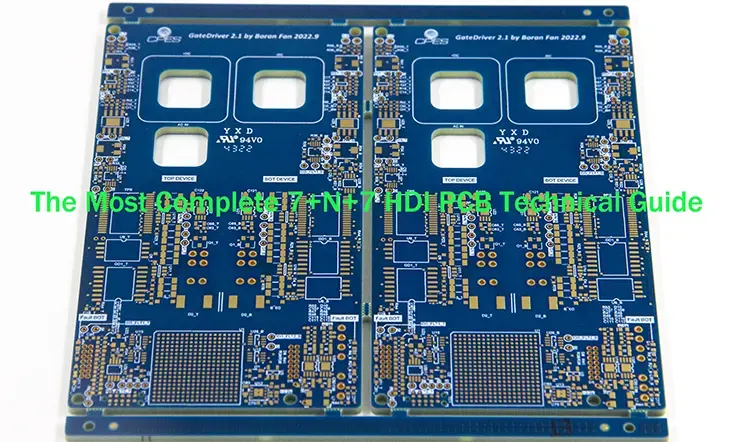
The requisition for high density interconnect (HDI) PCB has been on a consistent upward trajectory in the recent past. HDI technology allows for the integration of more components and circuitry in a smaller footprint, enabling the development of compact and high-performance electronic devices. One of the sophisticated HDI PCB designs available is the 7+N+7 stack up, which provides amplified functionality and reliability.
This post delves into the design, manufacturing process, distinct characteristics and benefits, It’s that 7+N+7 HDI PCB circuit boards offer, along with their application across diverse sectors.
Definition of HDI PCB
The term HDI PCB refers to High Density Interconnect Printed Circuit Board, a class of circuit boards specifically engineered to host a higher density of component and interconnections within a more compact space. HDI PCB are characterized by their advanced interconnect structures, such as microvias, buried vias and blind vias, which allow for more complex routing and increased circuit density.
HDI PCB carry a multitude of benefits over traditional PCB, manifesting shorter signal paths, reduced parasitic capacitance and inductance, along with regulated impedance characteristics that enhance signal integrity as well as overall electrical performance. Besides,HDI PCB also enable the use of smaller components with finer pitch, allowing for higher component counts and more compact designs.
HDI PCB are used in various industries. Such as consumer electronics, telecommunication, automotive, aeronautics and medical devices. Their compatibility is especially worth noting in circumstances needing miniaturization, high speed signal transmission and increased functionality, all whilst operating within confined space limitation.
Therefore, HDI PCB are an essential technology for achieving higher circuit density, improved signal integrity, and enhanced design flexibility in modern electronic devices.
Understanding 7+N+7 HDI PCB
7+N+7 HDI PCB are a specific type of HDI technology that offers even higher circuit density and design flexibility compared to traditional HDI PCB. Let’s break down the components of the term:
1. The “7” represents the number of layers in the core of the PCB. These layers typically consist of signal and power planes, allowing for the routing of signals and power distribution throughout the board.
2. The “N” exemplifies the quantity of stacked microvia layers. Microvias symbolize miniature drilled apertures that connect distinct layers of the PCB. Stacking microvia layers permits the enhancement of routing density and utilization of space more efficaciously.
3. The second “7” symbolizes the count of extra layers in the build-up strata. Build-up layers are leveraged to form complex interconnect structures, like blind vias and buried vias, which additionally enhance the circuit density and routing faculties of the PCB.
In essence, 7+N+7 HDI PCB comprise of a seven-layered core, stacked microvia layers (denoted by “N”), supplemented with another seven layers in the buildup layers. This structure empowers designers to achieve higher levels of integration, increased routing density, and improved signal integrity in a compact form factor.
The application of 7+N+7 HDI technology is exceptionally advantageous in setups demanding miniaturization, high speed signal transmission and advanced functionality. It facilitates the creation of intricate electronic systems with a reduced footprint, improved electrical performance and enhanced reliability.
Benefits and Applications of 7+N+7 HDI PCB
Benefits of 7+N+7 HDI PCB:
1.Increased Circuit Density: The layered stacking of microvias and build-up layer in 7+N+7 HDI PCB provides higher circuit density as opposed to the traditional PCB. This means the possibility of integrated more components within a reduced space, thus design the construction of more compact and less weighty electronic devices.
2. Enhanced Signal Integrity: In 7+N+7 HDI PCB, the incorporation of microvias and sophisticated interconnect structures contributes to the reduction of signal deterioration and the improve of signal integrity. This becomes predominantly vital in high speed applications where the upkeep of high frequency signal integrity is of critical importance.
3. Improved Thermal Management: The compact design of the 7+N+7 HDI PCB grants more proficient heat dispersion. The shorter signal paths and reduced layer count aid in minimizing thermal resistance, ascertaining superior thermal management and comprehensive system reliability.
4. The 7+N+7 HDI PCB provide more extensive design flexibility owing to the augmented routing density and enhanced pitch capabilities. Designers can realize complex routing patterns, closer component placement and complex circuitry, thus facilitating inventive and space conserving designs.
5. Reliability and Cost Savings: The sophisticated interconnect structures and enhanced routing in a 7+N+7 HDI PCB induce superior reliability. The reduced layer count and compact form factor further contribute to economic savings regarding material expenditure, fabrication intricacy and assembly time.
Applications of 7+N+7 HDI PCB:
1. Mobile Devices: The reduced magnitude and elevated circuit density of 7+N+7 HDI PCB render them perfect for portable apparatus like smartphones, tablets, and wearable technology. These PCB enable the integration of multiple functions and features in a small form factor.
2. High Speed Data Communication: 7+N+7 HDI PCB are favorably applicable for systems necessitating high speed data transmission, like network switches, routers and data center appliances. The improved signal integrity and lessened signal distortion ascertain reliable and excellent-performance data communication.
3. Aerospace and Defense: The reduced scale and high dependability of 7+N+7 HDI PCB render them appropriate for aerospace and defense utilization. These PCB can serve in avionics setups, radar configurations, communication infrastructures, and additional electronic constituents in aircraft and military apparatus.
4. Medical Devices: Medical devices frequently necessitate compressed and dependable PCB solutions. 7+N+7 HDI PCB can be employed in a range of medical devices, encompassing implantable instruments, diagnostic hardware, observed devices and medical imaging systems.
5. Automotive Electronics: The automotive industry is increasingly incorporating advanced electronics for safety, infotainment, and autonomous driving systems. 7+N+7 HDI PCB can be used in automotive applications where space is limited, and high reliability and signal integrity are essential.
How to Design and Manufacturing a 7+N+7 HDI Printed Circuit Boards?
Designing and manufacturing a 7+N+7 HDI PCB involves several steps and considerations.
1.Requirements Gathering:
Initiate by comprehending the project requirements, encompassing system specs, electrical performance preconditions, dimension restrictions, and any particular design guidelines or norms to adhere to.
2.Schematic Design:
Create a schematic diagram of the circuit, incorporating the positioning of components, signal paths and connections. Ensure appropriate signal integrity stipulations like impedance matching and controlled impedance necessities are met.
3.PCB Layout Design:
Use a PCB design software tool to create the layout of the PCB. Start by defining the layer stack-up, including the number and arrangement of signal, power, and ground layers. Place components, considering factors like signal paths, thermal management, and manufacturability. Utilize design rules and guidelines for trace width, spacing, and impedance control.
4.Microvia Planning:
Determine the microvia structure required for the design. Consider the aspect ratio, pad size, annular ring, and via pitch. Ensure that the microvia design meets the signal integrity requirements and can be manufactured reliably.
5.Routing:
Optimize the routing paths to accommodate the high-density interconnections. Use the available routing resources efficiently, considering signal integrity, power distribution, and thermal management. Follow design rules for trace width, spacing and impedance control.
6.Power and Ground Planes:
Allocate sufficient space for power and ground planes, ensuring low impedance paths for power distribution. Implement proper decoupling capacitors and ground stitching vias for noise reduction and power integrity.
7.Design Verification:
Perform design rule checks (DRC) and electrical rule checks (ERC) to ensure that the design meets the specified guidelines and requirements. Use simulation and analysis tools to verify signal integrity, thermal performance, and power distribution.
8.Design for Manufacturability (DFM):
Collaborate with your PCB manufacturer to ensure that the design is manufacturable. Address any manufacturing constraints or limitations early in the design process. Consider panelization, solder mask requirements, and other manufacturing considerations.
9.Design for Testability (DFT):
Incorporate test points, access points, and other features that aid in testing and troubleshooting. Ensure that the design is testable and can be efficiently tested during manufacturing.
10.Gerber File Generation:
Generate the necessary Gerber files, which contain the manufacturing information for the PCB fabrication process. These files include the PCB layers, solder mask, silkscreen and drill files.
11.PCB Manufacturing:
Send the Gerber files to a reliable PCB manufacturer. Choose a manufacturer with experience in producing high-density PCB and who can meet your specific requirements. Work closely with the manufacturer to address any manufacturing-related questions or concerns.
12.Assembly and Testing:
Once the PCB are manufactured, they can be assembled with the required components. Collaborate with an experienced assembly partner who can handle the high-density assembly and perform necessary testing and inspection to ensure quality.
How to Selection PCB Laminates for 7+N+7 HDI PCB Stack-ups?
Choosing the appropriate PCB laminates for 7+N+7 HDI PCB stack up is integral to securing the best electrical output and dependability. Here are some elements to ponder over while selecting laminates for your stack up:
1.Dielectric Material:
Select for a dielectric substance that presents apt electrical characteristics for high frequency application. The dielectric constant (Dk) and dissipation factor (Df) are pivotal aspects to think over. A lesser Dk value is typically favored for high speed design to cut down signal reduction and safeguard signal integrity. Moreover, a low Df value contributes to curtailing signal attenuation and preserving superior signal quality.
2.Thickness:
Determine the appropriate laminate thickness based on your design requirements. Thinner laminates allow for tighter trace spacing and smaller vias, enabling higher circuit density. However, thinner laminates may have higher signal losses and may require additional considerations for power distribution and thermal management.
3.Copper Foil:
Consider the type and thickness of the copper foil used in the laminate. More thick copper foils bestow enhanced current carrying capacity and can aid in controlling heat dispersion. Select the appropriate copper weight based on your power requirements and thermal considerations.
4.Glass Transition Temperature (TG):
TG is the temperature at which the laminate material transitions from a glassy state to a rubbery state. Select a laminate with a TG that exceeds the expected operating temperature of your PCB to ensure dimensional stability and reliability.
5.Thermal Conductivity:
For design with high power dissipation or thermal management requirements, contemplate laminates possessing superior thermal conductivity. These laminates can proficiently transfer heat away from essential components and improve overall thermal functionality.
6.Material Supplier and Quality:
Select a reputable laminate supplier known for producing high-quality PCB materials. Consider factors such as material consistency, reliability and availability. It’s important to ensure that the laminate materials meet industry standards and have the necessary certifications.
7.Compatibility with Fabrication Processes:
Verify that the selected laminates are compatible with the fabrication processes required for your design. Consider factors such as drillability, etchability, and adhesion properties to ensure smooth manufacturing and good quality control.
8.Cost Considerations:
Evaluate the cost of the selected laminates and consider your budgetary constraints. Balancing performance requirements with cost-effectiveness is important, but it’s crucial not to compromise on quality and reliability.
What is the Standard 7+N+7 HDI PCB Board Thickness?
The standard thickness for a 7+N+7 HDI PCB board can vary depending on the specific design requirements and application. Nevertheless, there is no established standard thickness for such a PCB stack up. The defining factors for thickness could include elements such as the tally of layers, the materials types, the desired electrical performance and any specific equipment constraints.
Commonly, HDI PCB are known for their high circuit density and compactness, which often leads to thinner PCB. The full thickness of a 7+N+7 HDI PCB stack-up extends between 0.6mm to 1.6mm (24mil to 63mil). However, this scope could be exceeded contingent on distinctive design requisites.
When deciding the suitable thickness, it is vital to factor in the electrical and mechanical regulations of your design. Elements like impedance control, thermal management, structural integrity and assembly discretion will have an impact on the optimal selection for the PCB thickness.
When designing 7+N+7 HDI PCB, it is recommended to work closely with your PCB manufacturer or professional PCB designer. They possess the capacity to advise and assist in identifying the ideal thickness that aligns with your specific design stipulations, bearing in mind the capabilities and limitations of the manufacturing processes and materials available.
Future Prospects and Challenges in 7+N+7 HDI PCB
The term 7+N+7 HDI PCB refers to multi layer printed circuit board characterized by several high density interconnections, principally encompassing microvias, buried vias and blind vias. These PCB provide increased routing density, diminished size, and superior signal integrity, rendering them suitable for an array of advanced electronic applications. Several factors come to the forefront when evaluating the forthcoming potential and challenges of 7+N+7 HDI PCB.
Miniaturization and Increased Functionality:
The need for more advanced electronic products is on the rise. 7+N+7 HDI PCB enable designers to pack more functionality into a smaller footprint, making them ideal for applications like smartphones, wearable, IoT device and medical equipment.
High Speed and High Frequency Applications:
As the requirement for high speed data transmission and high-frequency signal operations intensifies, 7+N+7 HDI PCB afford the necessary compactness in interconnection along with governed impedance features. These boards are apt for usage in spheres like telecommunications, data consolidation centers, high speed computational operations and wireless communication infrastructures.
Advanced Packaging Technologies:
7+N+7 HDI PCB are often used in advanced packaging technologies like flip-chip, chip-on-board (COB) and system-in-package (SiP). These technologies enable the integration of multiple components and subsystems into a single package, enhancing performance, reducing size and improving reliability.
Manufacturing Challenges:
As the complexity of 7+N+7 HDI PCBs increases, manufacturing challenges arise. The fabrication processes for microvias, buried vias, and blind vias require precise control and alignment. Achieving high yield and reliability in manufacturing can be a challenge, especially when dealing with smaller feature sizes and higher layer counts.
Signal Integrity and Power Integrity:
With the higher density of interconnects, signal integrity and power integrity become critical consideration. Proper design techniques, such as controlled impedance routing, decoupling capacitors, and power plane distribution, are essential to maintain signal integrity and prevent noise interference.
Cost and Time-to-Market:
The advanced technologies and manufacturing processes involved in 7+N+7 HDI PCB can lead to higher production costs. Additionally, the complexity of design and manufacturing may increase the development time, affecting the time-to-market for new products.
Materials and Reliability:
Choosing suitable materials possessing the correct dielectric attributes, thermal properties, and dependability is pivotal for 7+N+7 HDI PCB. Ensure the long term of these PCB under assorted operating circumstances poses a challenge that requires careful material selection and testing.
Despite the challenges the outlook for 7+N+7 HDI PCB looks bright. As the need for smaller, quicker and more efficient electronic devices grows the demand for PCB technologies like 7+N+7 HDI is expected to rise. Additionally ongoing progress in manufacturing methods, materials and design approaches will drive solutions to these challenges paving the way, for use of this type of PCB across different industries.
Final Words
As technological progression is ongoing, 7+N+7 HDI PCB board have established themselves as a pivotal technology in the realm of electronic design and fabrication. Their capacity for handling intricate and high density circuit design, coupled with enhanced signal integrity and reliability, render them perfect for a broad spectrum of applications. From consumer electronics to automotive, aerospace and defense sectors, the need for compact and high performance device is spearheading the adoption of 7+N+7 HDI PCB.

