The manufacturing process of PCBs is influenced by multiple factors, with the thickness being a key variable. The electrical conductivity and resistance of a PCB are significantly impacted by its thickness. Therefore, it is crucial for PCB manufacturers to carefully choose the appropriate thickness to ensure an optimal fit for a given application. Precision and accuracy in selecting the ideal thickness are essential for ensuring proper functionality and performance of the PCB.
Printed Circuit Boards (PCBs) are the backbone of modern electronic devices, serving as a platform for connecting and controlling various components on a circuit. Therefore, PCB thickness is a crucial factor in its design that can have a significant impact on performance, durability, and reliability. Different types of PCBs require distinctive thickness, and selecting the right thickness for your PCB is central to achieving optimal performance and longevity. In this article, we will provide an overview of standard PCB thickness, including the factors that impact it and how to choose the right thickness for your needs.
What Is PCB Thickness ?
PCB thickness refers to the overall depth or height of the printed circuit board. It is typically measured from the surface of the copper traces or planes on one side of the board to the surface on the opposite side. The thickness of a PCB affects its mechanical strength, electrical performance, and heat dissipation characteristics. Different types of PCB applications may have different requirements for thickness, and choosing the right thickness is important for ensuring optimum performance and reliability of the circuit board.
Many PCB contract manufacturers advertise 1.57mm or 0.062in as the standard PCB thickness. This reference is accurate to some extent, given that bakelite sheets were historically produced in this size during the early days of board fabrication. Consequently, this size has become the standard PCB thickness throughout history. Despite this standard, contemporary boards are available in varying sizes, both larger and smaller than the traditional 0.062in size. However, it is still widely accepted that 0.062in is the most common thickness for most designs.
In reality, there is now a range of common or standard PCB thicknesses available, including 0.031in (0.78mm), 0.062in (1.57mm), and 0.093in (2.36mm). Depending on the specific requirements of the job, custom-ordered boards with differing thicknesses can also be ordered from PCB manufacturers. PCB manufacturers must consider several factors during the design and manufacturing phase when determining the appropriate PCB thickness. The factors may include but not limited to:
Design Factors Influencing PCB Thickness
● Signal Types: The various signal types carried by PCBs have a direct impact on the selection of materials used for board production, and subsequently, the thickness of the board itself. For instance, PCBs that carry high power signals require thicker copper layers and wider traces, necessitating a significantly thicker board compared to low power signal boards.
Conversely, high-density PCBs that carry more complex signals tend to be thinner than other board types. This is due to the use of thin, high-performance materials and laser microvias, which allow for the creation of fine traces and higher density interconnections. PCB electronic engineers must be knowledgeable of these signal-specific board thickness requirements to select optimal materials and ensure efficient PCB design and development.
● Types of Vias: PCB vias play a critical role in the design process by routing traces through the-board, allowing for more compact and optimized designs. There are several types of vias available for such purposes, including:
● Micro via.
● Blind via.
● Buried via.
● Via-in-pad.
● Through via.
The choice of via type and its density can impact the PCB thickness required to accommodate them. For instance, thinner boards can utilize micro vias due to their smaller size and ability to support high-density connections. In contrast, larger or more widely-spaced vias will likely require a thicker board to maintain acceptable structural integrity. PCB electronic engineers must consider these factors to determine the optimal board thickness, ensuring successful design implementation and functionality.
● PCB Board Materials: For PCB manufacturers, the materials utilized in the fabrication of a PCB play a crucial role in determining the operational performance and lifespan of the board, as well as its thickness. The typical construction of a PCB consists of substrate, laminate, solder mask, and silkscreen; however, substrate and laminate are of particular importance in relation to board thickness. Both substrate and laminate are responsible for providing the foundation and structure of the PCB and, therefore, impact its overall thickness significantly.
The substrate material used may differ depending on the dielectric constant required, with options including paper and epoxy resin, glass weave, or ceramic. Laminates are constructed using a thermoset resin layered with paper or cloth. Both substrate and laminate offer various configurations, significantly impacting the circuit board’s thermal, mechanical, and electrical properties, as well as its overall thickness. PCB manufacturers must consider the desired performance requirements when selecting the optimal material configuration, balancing design goals with practical considerations to ensure the highest quality and most efficient results.
● PCB Copper Thickness: In PCB manufacturing, the thickness of copper utilized plays a vital role in the determination of the board’s overall thickness. The copper layer thickness is typically determined based on the amount of current that must flow through the PCB. The standard copper thickness for PCBs is between 1.4 and 2.8 mils (1 to 2 oz). However, specific board requirements may necessitate adjustments to these standards.
As thicker copper layers require additional materials and imposing processing challenges, they translate into a thicker board, and ultimately, a higher production cost. With the copper thickness being a major determinant of overall PCB thickness, manufacturers must make informed decisions about copper layer thickness to meet performance requirements while maintaining practical and economic constraints.
● Number of PCB Layers: As a PCB design engineer, it is crucial to consider the number of layers required, as this will significantly impact the board’s thickness. Two to six-layer PCBs typically fall within the standard PCB thickness range, but eight-layer and higher PCBs may require a non-standard thickness. While it may be possible to achieve standard thickness by using thinner PCB layers, this becomes increasingly impractical as the number of layers increases.
In the event of a design requiring more layers, it is advisable to accommodate a thicker PCB. On the other hand, if a design must adhere to specific thickness parameters but doesn’t require multiple layers, reducing the number of layers is recommended. By considering such crucial factors, PCB designers can develop effective designs that meet requirements for performance, practicality, and cost-effectiveness.
● Operating Environment: As a electronic manufacturer, it is crucial to acknowledge that a PCB’s thickness and materials greatly influence its conductivity and resistance, making it critical to select an appropriate thickness for specific environments.
For instance, a thin or flexible board may not be the best option for challenging operational conditions. Similarly, designing thicker copper traces may not prove suitable for high-current or thermally variable environments due to limited thermal stability. It is imperative to carefully evaluate the material and performance requirements of the connectors and components on the PCBs in relation to the board’s thickness. This evaluation helps designers reasonably determine whether a standard or custom PCB thickness is preferable, depending on the operational requirements, practicality, and cost-effectiveness.
However, the design process does not end here; manufacturers must also play an active role in the process to discuss their capabilities and limitations and how these may impact the final PCB design. Effective collaboration between designers and manufacturers facilitates the development of high-quality PCBs that meet the desired performance requirements while remaining viable and cost-effective.
The Influence of PCB Thickness in the Manufacturing
● Layer Count: As a PCB designer, it is essential to recognize that more layers on a board can make it increasingly difficult to achieve a standardized thickness during manufacturing. While some specialty manufacturers may be capable of creating stacked PCBs with thinner layers to meet specific thickness requirements, this capability may not be universal and often comes with an associated cost increase.
It is imperative to consult with the manufacturer before finalizing the board design to gauge their capabilities and determine what they can achieve in terms of layering requirements. Conducting these discussions before finalizing the design helps identify and address any potential issues in advance, ensuring that the design meets all necessary specifications. Moreover, effective collaboration between designers and manufacturers helps deliver high-quality PCBs that achieve the desired performance goals while remaining practical and feasible in terms of manufacturing and costs.
● Copper Thickness: As a PCB manufacturer, it is crucial to acknowledge that etching is one of the most crucial steps in PCB fabrication for creating copper traces. The thickness of the internal copper layer directly impacts the etching and plating manufacturing processes. Consequently, thicker copper layers will have a notable impact on the overall PCB manufacturability, which can potentially affect the board’s design and production cost. It is therefore essential to consider the copper layer thickness during the initial design stage to ensure the chosen thickness meets the manufacturing process’ requirements and remains within the available budget.
By working closely with designers to evaluate copper thickness requirements, manufacturers can deliver high-quality PCBs that meet the necessary performance goals while remaining feasible and cost-effective.
● Drill Hole Equipment: As a PCB manufacturer, it is crucial to recognize that while drill hole size and spacing are vital considerations in achieving performance goals, drilling holes in PCBs introduces a new layer of complexity in the manufacturing process. Manufacturers face limits in drilling holes through the thickness of the board, which are determined by milling machines and lasers’ diameter and depth. This limit is represented by an aspect ratio, which is the ratio of the hole’s depth to the diameter of the drill hole. For standard drilling, all manufacturers should be able to achieve a 7:1 aspect ratio.
However, some manufacturers may achieve a higher aspect ratio, but this will raise the board’s cost and needs to be discussed with the manufacturer before finalizing the board design. Thicker boards can limit manufacturers’ ability to drill smaller diameter holes. By considering the aspect ratio limitations during the design stage, designers can develop an effective design that accommodates the necessary performance requirements while remaining practical and cost-efficient. Effective collaboration between designers and manufacturers further ensures the production of high-quality PCBs that match the desired performance profile.
● Depanelization Method: As a PCB manufacturer, it is critical to acknowledge that depanelization is another crucial manufacturing consideration. Typically, PCBs are fabricated on large panels containing several boards that are later separated to create individual boards. The thickness of the board influences the depanelization method utilized. For instance, thicker boards necessitate careful scoring, whereas thinner boards may be routed to create breakaway tabs. To optimize depanelization, it is vital to work closely with the manufacturer and discuss the various depanelization techniques as well as any unique depanelization requirements.
It is essential to engage the manufacturer in these discussions before completing the final PCB design since these manufacturing factors are dependent on the manufacturer’s capabilities, methods, and associated costs. Failure to discuss these elements earlier in the design process can result in modifications or complete redesigns of your layout, leading to additional costs. Therefore, PCB manufacturers must collaborate effectively with designers and provide critical input on manufacturing requirements to ensure a smooth production process that produces high-quality and cost-efficient PCBs.
Standard PCB Thickness Types
Standard PCB thickness can vary depending on the specific type of board and its intended application. Here are some typical thickness values for various types of PCBs:
● Single-layer PCB thickness: Between 0.4 mm and 1.6 mm.
● Double-layer PCB thickness: Between 0.8 mm and 2.4 mm.
● Multi-layer PCB thickness: Between 0.6 mm and 3.2 mm.
● Rigid-flex PCB thickness: Between 0.2 mm and 2.0 mm.
● High-speed PCB thickness: Between 0.6 mm and 2.4 mm.
These values are considered standard in the industry and are used by PCB manufacturers as a guide in the design and production of circuit boards. However, it’s essential to consider the specific requirements of each application to ensure the selected thickness is appropriate for the performance and reliability needed. Additionally, custom thicknesses may be required in unique cases, such as those with specific design constraints or unusual requirements for thermal management or structural support.
Considerations When Choosing PCB Thickness
Choosing the appropriate PCB thickness depends on various factors, such as the complexity of the circuit design, board size, component density, thermal management requirements, and mechanical constraints. Here are some factors to consider when selecting the right PCB thickness:
● Mechanical strength: If the PCB will be subjected to stress or external loads, it’s important to have enough thickness to ensure mechanical strength and avoid bending or breaking.
● Component density: High-density PCBs or those with large components may require thicker thickness to accommodate the component height and prevent interference between them.
● Thermal management: For applications with high power dissipation or significant heat generation, a thicker PCB can provide better thermal performance by allowing for more effective heat dissipation.
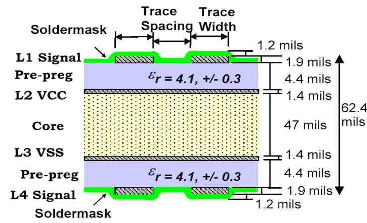
● Electrical properties: The thickness of the PCB can influence impedance, signal integrity, and electrical properties. It is critical to match the board thickness to the impedance. This is due to the fact that the thickness of the board is actually the thickness of the dielectric, and the dielectric aids in impedance control. Therefore, the selected thickness must meet the specified requirements of the circuit design.
● Cost and manufacturing: Thicker PCBs may be more expensive and require additional manufacturing steps that can affect the cost and time to manufacture the board.
● Equipment Capabilities: When manufacturing PCBs, it is critical to evaluate whether the manufacturer has the necessary equipment to achieve the desired board thickness. Moreover, if an application requires intricate features that can only be realized through advanced design techniques, it is crucial to identify manufacturers who can meet such requirements as early as possible.
However, such techniques generally come with added costs that need to be taken into account. By prioritizing a deep understanding of client requirements during the design phase, manufacturers can effectively match client needs with production capabilities, while also ensuring a cost-effective outcome. Effective collaboration between manufacturers and clients is essential in developing and delivering high-quality PCBs that accurately align with all specifications, such as performance, manufacturing, and budget.
Turnaround Time: In PCB manufacturing, standard thicknesses present minimal difficulties, and the production process requires very few adjustments. However, for custom thicknesses, adjustments are necessary, which can significantly increase production time. Adapting existing equipment settings and processes to fit the custom design requirements can be time-consuming and affect the manufacturing schedule, potentially delaying turnaround time.
If the design includes complex features, this will further increase the manufacturing time. Therefore, when considering a custom PCB thickness, it is crucial to engage with the manufacturer to obtain an accurate estimate of the time required for its production. By liaising with the manufacturer, clients can adjust their delivery timelines accordingly, preventing any uncertainty or delays. Collaborative communication between manufacturers and clients is essential in developing high-quality, custom PCBs that precisely match performance requirements while remaining feasible in terms of manufacturing time and budget constraints.
● Additional Cost: As experienced PCB engineers, it is crucial to carefully evaluate the cost-effectiveness of producing a custom circuit board for your company. Standard-thickness boards offer significant advantages, including reduced manufacturing costs and avoidance of potential delays associated with custom-thickness boards. Therefore, it is imperative to make a thorough analysis of the cost-benefit trade-offs before deciding on a custom-thickness board. While it is true that using special materials to accommodate a standard thickness may be more expensive, it could potentially outweigh the costs associated with modifying a custom-thickness board. It is essential to take all relevant factors into account and make a well-informed decision that aligns with your company’s goals and requirements.
So, selecting the right PCB thickness requires consideration of various factors that impact the performance, reliability, and manufacturing of the board. The selected thickness should meet the specific needs of the application while balancing design requirements, manufacturing costs, and other practical considerations.
Conclusion
PCB thickness standards vary according to the type of board and intended application, and custom thicknesses may be required in some cases. Ultimately, selecting the appropriate PCB thickness requires balancing the requirements of the intended application with considerations of manufacturing cost, design complexity, and other practical considerations.
It is evident in the PCB industry that PCB thickness plays a vital role in ensuring the necessary functionality of a printed circuit board. As PCB manufacturers, we understand this and strive to provide accurate results for the best performing PCBs to our esteemed clients.
We value every customer’s investment in purchasing a PCB and appreciate the trust bestowed upon us. Hence, we leverage our extensive experience and cutting-edge technology to design PCBs that adhere to our client’s specified standard thicknesses.
Should you have any questions about PCBs, PCB manufacturing, or the PCB assembly process for your project, our team is available to assist you 24/7. Most importantly, we take pride in delivering critical high-performance PCB and PCBA solutions to our clients’ doorsteps, ensuring their satisfaction every step of the way.
Related Posts:
1. Selecting PCB Laminate Materials: A Comprehensive Overview
2. PCB Copper Trace Width and Space: Everything You Need to Know About Them
3. Which Types are Most Commonly Used in PCB Substrates?
4. What Is Fiberglass PCB and Why Fiberglass Used in PCB Manufacturing?