
Printed circuit board switches are widely used in electronic systems where precise control, compact layout, and long-term reliability are expected. The process of integrating these components is not limited to part selection—it extends across mechanical design, contact material choices, layout practices, signal behavior, and manufacturing compatibility.
This engineering guide presents a structured walkthrough of PCB switch technologies, from tactile and push-button switches to rotary and DIP types. It explains interface designs used in consumer electronics, automotive assemblies, and medical-grade devices. core layout topics include switch placement, trace clearance, actuation force, bounce mitigation, and strategies for managing crosstalk in multilayer or rigid-flex configurations.
You will also find detailed descriptions of surface mount and through-hole assembly techniques, quality inspection tools such as AOI and ICT, and typical fault scenarios like intermittent contact or overheating. To close the loop, the guide outlines rework practices, DIP switch configuration, and turnkey service models suited for engineers and original equipment manufacturers.
Understanding PCB Switch Technology, Function, and Applications
In modern electronics, PCB switches are integral components that help control and interact with electronic circuits. These switches, mounted directly onto a PCB, offer a streamlined design that improves device performance, simplifies assembly, and enhances user experience. Let’s explore their role, common uses, and how they contribute to various industries.
What Is a PCB Switch and Its Role in Circuit Design?
A PCB switch is a type of electromechanical component that is directly mounted onto a printed circuit board. When activated, it either completes or breaks an electrical circuit, controlling the flow of electricity. Unlike traditional switches that may be externally connected, PCB switches offer a more compact and reliable solution for modern electronic designs.
Key Features-
●Integration: PCB switches are built directly into the PCB, reducing the need for additional wiring and components, improving overall circuit efficiency.
●Variety: These switches are available in various forms such as tactile, push-button, slide, and rotary types. This range of options makes it easier to match a switch to the specific demands of each application.
●Customization: Switches can be configured with features like backlighting, varied actuation forces, and tactile feedback, giving more flexibility in crafting user-friendly interfaces across different projects.
Using PCB switches in circuit design can help reduce component count, improve reliability, and ensure that circuits are more streamlined, making them a staple in contemporary electronics.
Applications in IoT Devices, Automotive, Medical, and Consumer Electronics
PCB switches are found in a wide range of applications, from consumer electronics to highly specialized industries like automotive and medical technology. Here’s a look at how they are used:
1. IoT Devices-
●Smart Home Devices: Smart lights, thermostats, and home security systems often rely on PCB switches to handle user inputs. The switches provide a simple and effective way to control complex systems.
●Wearable Devices: Small, compact PCB switches are commonly used in wearables like fitness trackers and smartwatches, where limited space demands components that support multiple functions efficiently.
2. Automotive Industry-
●Dashboard Controls: From the control of air conditioning systems to the operation of infotainment systems, PCB switches are integrated into the dashboard and other areas of vehicles to manage various functions.
●Steering Wheel Controls: Many modern vehicles integrate PCB switches into the steering wheel to manage main systems like volume, cruise control, and hands-free communication.
3. Medical Equipment-
●Diagnostic Machines: In medical devices, such as blood analyzers and diagnostic equipment, PCB switches ensure smooth operation, offering precise control over machine functions.
●Patient Monitoring Devices: These devices often rely on PCB switches to allow healthcare professionals to adjust settings, ensuring accurate readings and adjustments.
4. Consumer Electronics-
●Television Remotes and Controllers: Reliable PCB switches are found in TV remotes and home entertainment systems, where long-lasting performance is necessary.
●Game Consoles and Controllers: In gaming devices, switches are a part of the user interface, helping to provide responsive and durable controls.
The broad range of applications highlights how PCB switches provide practical, efficient solutions for a variety of industries, meeting the specific needs of each sector.
Enhancing Human-Machine Interaction (HMI) with PCB Switches
Human-Machine Interaction (HMI) focuses on making devices more intuitive and responsive for the user. PCB switches play a reliable role in this by offering precise, tactile feedback and a streamlined way for users to interact with their devices. They are designed to be both functional and comfortable, improving how users control and experience their devices.
Advantages-
●Tactile Feedback: Many PCB switches include features that give users a clear, tactile response when activated. This feedback ensures that users know when their input has been registered, improving accuracy.
●Customizable Designs: These switches can be designed to match the device’s aesthetic, allowing manufacturers to create cohesive product designs that align with the overall look and feel of the device.
●Durability: PCB switches are built for durability, maintaining performance even in high-use environments. In both industrial settings and consumer electronics, these switches are designed to handle repeated operation.
Case Study Example:
For industrial control panels, PCB switches with integrated LEDs enhance visibility and reduce operator errors, especially in low-light environments. This design choice not only boosts functionality but also improves safety and efficiency in operations.
Comparison of PCB Switch Features:
| Feature | Traditional Switches | PCB Switches |
| Mounting Style | External mounting | Direct PCB mounting |
| Size | Larger | Compact |
| Customization | Limited | High flexibility |
| Assembly Complexity | More complex | Streamlined |
PCB switches provide several advantages over traditional types, such as easier integration, a smaller footprint, and customizable functionality. These traits help enhance both layout flexibility and user interaction in modern electronic products.
PCB Switch Types: Choosing the Right Switch for Your Circuit
When designing a PCB, selecting the right switch can shape the overall performance and functionality of your device. The type of switch used will directly impact the way users interact with your product, as well as how the circuit operates. Understanding the various types of PCB switches can help make the right decision based on the intended application, ensuring a smooth, efficient user experience and an optimized design.
Tactile Switches vs. Push Button Switches: Which to Use?
Tactile switches and push-button switches are both popular options, but they offer distinct features. Knowing how they differ helps in selecting the most fitting type for your specific design needs.
●Tactile Switches: These switches provide users with tactile feedback, such as a “click” when pressed. This response assures users that their action has been registered. Tactile switches are used in applications where precise user feedback is required, like remote controls or mobile device buttons. They are favored for their high reliability and the positive feedback they provide during operation.
●Push Button Switches: Push-button switches are simpler in design. They are typically used for basic on/off functionality and are often found in situations where feedback is not as critical, such as in power buttons for appliances. These switches are robust, straightforward, and usually cost-effective.
Which to Choose-
●Tactile switches are great for applications requiring clear user feedback, such as communication devices, control panels, and consumer electronics.
●Push-button switches work best in simpler devices that only require a basic toggle action, like turning a device on and off.
Slide, Toggle, Rotary, and DIP Switch Variants
PCB switches come in different styles, each suited for specific tasks or environments. Here’s a breakdown of the variants and what makes them unique:
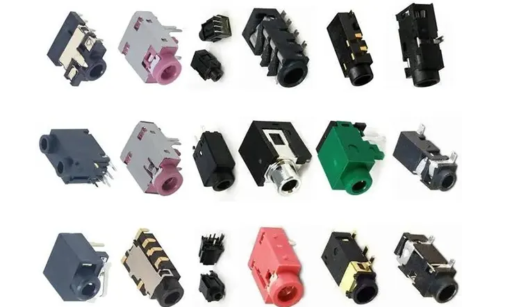
●Slide Switches: Slide switches are compact and easy to use, making them suitable for small devices like toys, audio equipment, and medical devices. They offer simple on/off functionality and can be used in applications that require minimal switching action.
●Toggle Switches: Toggle switches provide a more tactile action with a flipping motion. These switches are commonly used in industrial applications where users need to operate heavy-duty equipment. They are easy to understand and provide a clear visual indicator of their position, making them better for control systems.
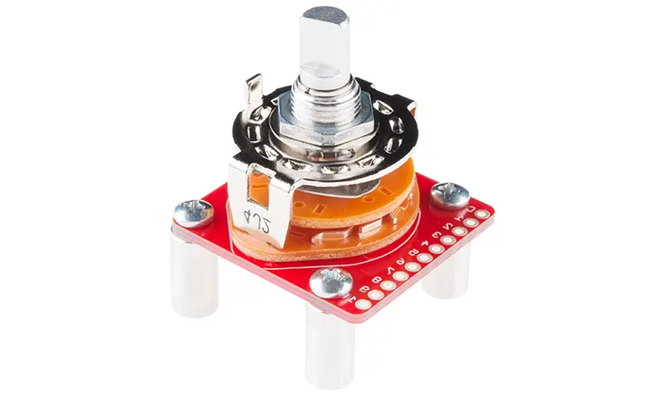
●Rotary Switches: Rotary switches allow users to select a range of settings by turning a dial. These are often used in devices like radios, mixers, and various control panels. The adjustable settings provide flexibility, allowing users to make fine adjustments.
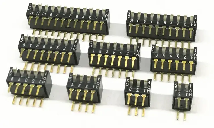
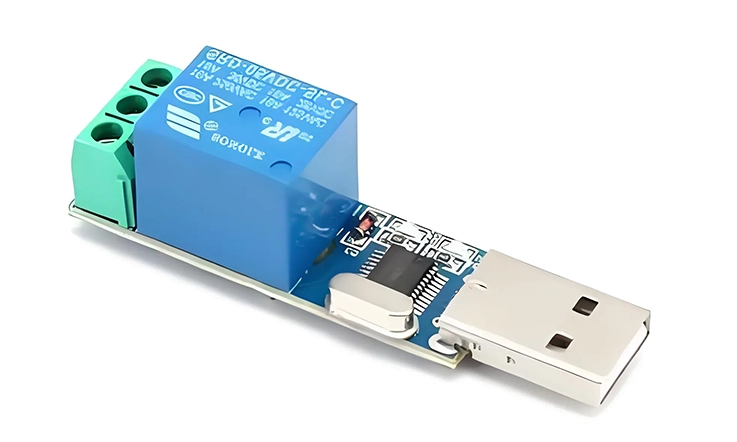
●DIP (Dual In-line Package) Switches: DIP switches are small switches with multiple on/off positions and are commonly used in scenarios where space is limited but several different options need to be configured. They are frequently used in computer hardware, networking devices, and embedded systems.
Which to Choose-
●Slide switches are perfect for small devices with limited switching needs.
●Toggle switches are suitable for high-durability environments where visibility of the switch’s position is necessary.
●Rotary switches work well for adjusting multiple settings in audio or industrial equipment.
●DIP switches are great for compact devices requiring multiple switch configurations.
Hot-Swappable vs. Permanent Switch Types in PCBs
Selecting between hot-swappable and permanent switches affects both the device layout and how the interface behaves over time.
●Hot-Swappable Switches: These switches are designed to be replaced while the system is powered on, offering a convenient option for devices that require maintenance or upgrades without turning off the power. Hot-swappable switches are common in high-end electronics, like servers and modular systems, where minimal downtime is required.
●Permanent Switches: As the name suggests, permanent switches are meant to stay fixed throughout the life of the product. These switches are typically used in devices where the configuration doesn’t need to change once set up, such as home appliances, basic electronics, or non-upgradable systems.
Which to Choose-
●Hot-swappable switches are beneficial in systems that demand flexibility and quick maintenance, like in servers or computing systems.
●Permanent switches are more suitable for devices like kitchen appliances or simple consumer electronics, where no part of the circuit requires regular modification or updates.
Materials Used in PCB Switches: Conductivity, Durability, and Performanc
The materials chosen for PCB switches directly impact their functionality, longevity, and how well they handle the demands of their respective applications. With the right material, a PCB switch can offer reliable performance over time, even in challenging environments. Let’s explore the materials used in PCB switches and how they influence main factors such as conductivity, durability, and overall performance.
Contact Materials: Gold-Plated, Silver, and Carbon
The contact materials in PCB switches influence how reliably they conduct electricity when activated. Each material type brings its own characteristics, making certain options more compatible with specific environmental or usage conditions.
●Gold-Plated Contacts: Gold is one of choices for high-performance switches due to its excellent electrical conductivity and resistance to corrosion. It ensures that electrical connections are stable over long periods and remains reliable in environments where oxidation could be a problem. This makes gold-plated contacts ideal for high-end applications, such as in medical devices, aerospace equipment, and high-quality consumer electronics. While gold plating adds cost, it also delivers long-term stability.
●Silver Contacts: Silver is a conductive material frequently used in PCB switches, though it can tarnish over time when exposed to air. This surface change may impact the electrical path slightly, but silver remains a widely used option for general-use circuits. It often appears in consumer electronics and other devices where budget and function are balanced. While it doesn’t hold up as long as gold in some cases, it still provides steady conductivity in many routine applications.
●Carbon Contacts: Carbon-based contacts are more affordable than gold and silver, offering a practical solution for switches in lower-cost products. They are resistant to oxidation, making them a good option for environments where minimal wear is required. Carbon switches are typically used in devices like remote controls, simple appliances, and some consumer electronics. However, they don’t offer the same level of conductivity or lifespan as gold or silver contacts.
Choosing the Right Contact Material-
●Gold-plated contacts are a good fit for demanding applications where long-lasting, corrosion-free performance is necessary.
●Silver contacts are often chosen when a balance between cost and conductivity is needed.
●Carbon contacts work well for budget-conscious applications where durability isn’t a primary concern.
Dome, Membrane, and Mechanical Switch Construction
The construction of a switch affects both its tactile feedback and overall durability. Each switch construction type is designed for specific needs and environments. Let’s take a look at the different switch constructions commonly used in PCB designs.
●Dome Switches: Dome switches are frequently used in compact electronic devices, providing a satisfying tactile response when pressed. These switches feature a metal dome that compresses when pressed, creating a click that lets the user know their input has been registered. Dome switches are found in many consumer devices like calculators and remote controls, where space is limited, and a soft feedback is necessary. While they provide cost-effective performance, they can wear out faster compared to more durable switch types.
●Membrane Switches: Membrane switches are built from flexible layers, often using polyester or polycarbonate, with printed circuitry that responds to surface pressure. Their slim structure makes them suitable for setups that need sealed interfaces. These switches are frequently used in industrial equipment, medical tools, and kitchen devices due to their resistance to dust and moisture. With reliable durability and cost-friendly production, membrane switches fit well into many household and everyday electronic products.
●Mechanical Switches: Mechanical switches use individual moving parts like springs and metal contacts to register a press. These switches are known for their robust construction and are used in environments where precise, consistent feedback is necessary. Mechanical switches are found in products like gaming keyboards, industrial control panels, and automotive equipment, where user input needs to be clear and precise. These switches tend to last longer than dome and membrane switches, providing excellent tactile feedback over time.
Which Switch Construction to Choose-
●Dome switches are great for affordable and compact devices with simple, short-term use.
●Membrane switches are perfect for applications that require a sealed switch to prevent the ingress of dust or liquids.
●Mechanical switches should be selected when a precise, long-lasting feedback mechanism is necessary for high-use environments.
Environmental Resistance: IP Ratings, Temperature, and ESD Protection
PCB switches must perform in diverse conditions, from extreme temperatures to exposure to static electricity. Choosing the right switches with the necessary environmental resistance features will ensure reliability, no matter the conditions. Here’s an overview of the environmental factors to consider when selecting PCB switches.
●IP Ratings (Ingress Protection): IP ratings indicate how well a switch can resist dust and water. The first digit in the rating represents the level of protection against solid objects like dust, while the second digit indicates protection against liquids. For example, a switch with an IP67 rating is fully dustproof and can be immersed in water up to 1 meter deep. IP-rated switches are perfect for outdoor equipment, industrial machinery, or other applications where exposure to dirt and moisture is a concern.
●Temperature Resistance: Depending on the application, PCB switches must perform reliably within defined temperature ranges. Most standard models are designed to function between -20°C and +85°C. However, certain environments—like those found in automotive or aerospace systems—may demand units that can handle more extreme heat or cold. Selecting a switch with a temperature rating that matches the real-world conditions it will encounter helps ensure consistent performance.
●ESD Protection (Electrostatic Discharge):ESD protection is necessary for devices where static discharge could lead to malfunctions or damage to sensitive components. For products intended for environments prone to static buildup, opting for switches with built-in ESD protection is a practical choice. These switches are designed to release electrostatic charges, safeguarding both the switch and the device from potential harm.
Choosing the Right Environmental Features-
●IP-rated switches are best for devices used outdoors or in environments where exposure to dust and water is expected.
●Temperature-resistant switches should be chosen for devices that will face high or low-temperature conditions, such as automotive electronics or machinery.
●ESD-protected switches are a must in sensitive applications, such as medical devices or computers, where static discharge could cause failure.
PCB Switch Design Guidelines: Footprint, Clearance, and Routing
Designing PCB switches means balancing mechanics, electrical constraints, and layout techniques that follow established manufacturing logic. Component spacing, routing discipline, and contact behavior all shape how your PCB behaves during real-world use. This section takes a deeper dive into layout, mechanical switch dynamics, and signal behavior without relying on buzzwords.
H3:PCB Layout Best Practices for Switch Placement
When setting up your PCB layout, switch positioning can affect signal timing, tactile interaction, and EMI performance. The arrangement needs to support manufacturability and user-facing applications like HMI or input control.
●Group by Function: Align components in zones, separating logic signals from power lines. This practice keeps things cleaner and helps cut down on interference.
●Clearance and Edge Space: Keep at least 1.27mm (~50 mils) between the PCB edge and switch terminals. This gap allows space for enclosures, connectors, and automated tooling.
●Orientation: Maintain uniform alignment for switches and polarized components to support optical inspection and lower human error during assembly.
●Switch Access: Switches for testing or operation should stay accessible on the top layer, and not be tucked under displays, connectors, or shielding.
Routing traces should maintain minimum length while avoiding tight corners and high-angle bends. Copper pour zones near the switch can help stabilize voltage rails and reduce ground bounce.
H3:Actuation Force, Travel Distance, and Tactile Feedback Design
Mechanical properties of a switch affect how users experience your product. Different industries lean on different specs:
●Actuation Force: Light press options (under 60g) work well for portable devices, while industrial gear may require heavier forces (up to 200g).
●Travel Distance: Short throw designs offer faster response in consumer electronics, while long-travel switches give more defined feedback for control panels or machinery.
●Tactile Response: Snap domes or mechanical stems introduce a physical “bump” that signals contact closure without visual cues.
| Property | Consumer Electronics | Industrial Applications |
| Actuation Force | Under 60g (light press) | Up to 200g (heavier press for durability) |
| Travel Distance | Short throw designs for quick response | Long travel switches for more tactile feedback |
| Tactile Response | Snap domes or mechanical stems for physical “bump” | Carbon-contact domes for durable feedback |
Choosing the right actuation feel isn’t guesswork — it depends on environment, interface design, and the need for repetitive interaction without fatigue. You might go with scissor switches for wearables, or carbon-contact domes in sealed touchpads.
H3:Managing Electrical Noise, Crosstalk, and Bounce Issues
Noise, bounce, and coupling aren’t just high-frequency problems — they can affect simple switches too, especially when routing runs close together or lacks shielding.
●Minimize Crosstalk: Route switch signals perpendicular to nearby high-speed traces. If they’re too close and parallel, you could see voltage spikes on input pins.
●Keep Signals Quiet: Place series resistors near the switch terminals to suppress overshoot. Route signals over solid ground planes for stability.
●Address Bounce: Switch bounce can cause false triggering. Use capacitor filters, Schmitt triggers, or debounce firmware to smooth out the chatter.
Avoid excessive via stitching near switch pads, since that could create return path breaks or inductive loops. Also, keep traces short between the switch and microcontroller — no one wants ghost inputs when EMI kicks in.
H2:Switches in Rigid-Flex and Multilayer PCB Design
Designing switches into rigid-flex and multilayer PCBs is an intricate task that requires careful consideration of mechanical, electrical, and spatial constraints. Rigid-flex PCBs combine the advantages of both rigid and flexible circuit board designs, allowing for complex configurations while maintaining flexibility and space-saving potential. Multilayer PCBs offer a compact way to handle high-density designs, where switches must be integrated seamlessly into the layers. Let’s dive into the specifics of incorporating switches into these advanced PCB designs.
H3:Mechanical Constraints and Layer Stackup Strategy
When working with rigid-flex PCBs, one of the first things to keep in mind is the mechanical limitations. Flexible sections, which need to bend, must remain thin, yet strong enough to withstand the mechanical stress of repeated movement. Rigid areas, on the other hand, need more layers for supporting components and maintaining structure.
| Design Element | Recommended Value/Choice | Notes |
| Flex Section Layers | 1–2 conductive layers | Keeps flexibility high, avoids stress accumulation |
| Rigid Section Layers | Up to 6 layers | Supports denser circuitry and switch mounting |
| Bend Radius | 6× to 10× flex thickness | Prevents conductor strain and solder joint damage |
| Flex Material | Polyimide | Excellent thermal and mechanical durability |
| Rigid Material | FR-4 or equivalent | Supports mechanical strength and complex layouts |
●Layer Stackup Design: In a rigid-flex PCB, the stackup should be divided so that the rigid sections can handle the most complex components while the flex sections stay flexible. A typical stackup might consist of two to four layers in the flex area, and up to six in the rigid parts. The flexible part should not exceed one or two conductive layers to maintain flexibility.
●Material Consideration: Polyimide is commonly chosen for the flexible part of the PCB due to its excellent flexibility, resistance to heat, and ability to handle a variety of environmental conditions. For the rigid sections, FR-4 or similar materials are often used, as they are capable of supporting more intricate designs and heavier components.
●Flexibility and Bend Radius:In rigid-flex PCBs, maintaining an appropriate bend radius is necessary to prevent stress-related failures. The flex sections typically require a minimum bend radius between six to ten times their thickness. When the radius is too tight, it can strain the conductor and compromise solder joints, leading to mechanical issues over time.
H3:Flexible Interface Solutions in Consumer Electronics
Flexible PCB designs are increasingly popular in consumer electronics due to their compact form and ability to handle mechanical stress. In smartphones, wearables, and other portable devices, flexible PCBs provide solutions that standard rigid boards cannot match. Here’s how switches can be incorporated into flexible PCBs for use in consumer products:
| Design Aspect | Recommendation | Purpose |
| Switch Placement | On rigid sections only | Prevents damage from repeated bending |
| Routing Layout | Curved and optimized in low-stress zones | Reduces trace fatigue and electrical failure |
| Coverlay Material | Polyimide | Resists dust, moisture, and mechanical wear |
| Coverlay Thickness | 25–50 µm | Balances flexibility with mechanical protection |
| Common Applications | Wearables, smartphones, handheld devices | Leverages space efficiency and durable switch integration |
●Switch Placement:In flexible PCBs, switches should not be located in regions that undergo repeated bending. Such placement may strain the electrical joints or damage the mechanical structure of the switch itself. A more stable outcome can be achieved by mounting switches on the rigid zones of the board, where stress from flexing is minimal.
●Routing Strategies: Flex PCBs benefit from the ability to route traces in compact, curved layouts that would be difficult to achieve with rigid boards. Careful routing ensures that the traces do not experience stress and that the switch remains functional throughout the life of the device.
●Protective Coverlays: Coverlays, which are protective layers that cover the flexible parts of the PCB, prevent the circuit from damage while maintaining the flexibility of the design. These coverlays often include a layer of polyimide for protection against dust, moisture, and mechanical abrasion, which is especially beneficial in consumer electronics.
H3:Routing Switches on Dense Multilayer Boards
In multilayer PCBs, managing the routing of switches is often one of the most challenging tasks due to the dense nature of the design. Multilayer PCBs allow for high-density component packing, but they also introduce issues with signal integrity, cross-talk, and electromagnetic interference. Here’s how to successfully route switches in such designs:
| Parameter | Best Practice | Impact |
| Layer Configuration | Alternate signal and ground layers | Maintains stable signal paths and minimizes EMI |
| Signal Layer for Switches | Dedicated inner signal layers | Limits crosstalk and isolates noisy paths |
| Via Placement | Avoid in flex areas; place near low-stress zones | Preserves structural and electrical integrity |
| Via Size | ≤ 0.3 mm (microvias preferred) | Saves space and reduces impedance discontinuities |
| Impedance Control | Match trace width to dielectric thickness | Supports clean transmission for high-speed switch signals |
●Layer Stackup: In multilayer boards, arranging signal and ground layers in an alternating pattern is a standard approach to support stable electrical performance. This configuration helps reduce unwanted interference and maintains cleaner signal paths, especially in high-frequency designs. When dedicated signal layers are used for switch routing, it becomes easier to manage spacing and limit the impact of cross-talk between nearby traces.
●Via Management: Vias should be strategically placed in areas where mechanical stress is less likely to occur. In flexible areas, vias should be avoided altogether to maintain the integrity of the flexible section. Additionally, it is essential to keep via sizes as small as possible to preserve space and minimize signal loss.
●Impedance Control: For high-speed signal paths, maintaining consistent impedance is necessary to support clean transmission and reduce signal issues like reflection or distortion. This can be managed by adjusting the trace width and controlling the spacing between signal and ground layers, especially when designing switch routing for circuits operating at higher frequencies.
PCB Switch Manufacturing Process
Manufacturing PCB switches is a meticulous process that requires precise attention to detail at every stage, from the prototype phase to mass production. Each phase in the manufacturing workflow must be executed with high standards to ensure quality, reliability, and efficiency. Let’s break down the entire journey of PCB switch manufacturing, detailing the steps involved, the inspection methods used to guarantee performance, and the specialized techniques for programming DIP switches.
Step-by-Step Switch Manufacturing Workflow
The manufacturing of PCB switches begins with a well-structured workflow, which ensures that each step is executed with precision and meets the required specifications. Here’s an overview of the typical process:
1.Design and Prototype: The first stage involves the creation of the PCB switch design. The design team collaborates with clients to define usage scenarios and performance expectations. After confirming the layout, a prototype is produced. This phase allows for checking mechanical alignment, electrical behavior, and how well different switch types—such as tactile, membrane, or DIP—work within the overall design.
2.Material Selection: After the design is confirmed, materials are carefully chosen. Contact materials like gold-plated or silver are selected based on their conductivity and durability. The flexible or rigid base materials (e.g., FR-4, polyimide) are also chosen at this stage, taking into account the intended environment and load conditions.
3.Layer Creation: For multilayer PCB designs, individual layers are fabricated, including the conductive traces and vias. Special care is taken during this phase to ensure that switches will be placed correctly without any electrical interference or physical stress.
4.Switch Assembly: The switch components are then assembled onto the PCB. This involves automated placement of components like tactile switches, push-button switches, and DIP switches using high-precision pick-and-place machines. Some switches may also require manual soldering depending on their complexity or size.
5.Soldering and Bonding: The components are then soldered onto the PCB. Soldering methods such as wave soldering or reflow soldering are applied, depending on the type of switch and board design. For more specialized applications, manual soldering is used for quality assurance.
6.Encapsulation and Coating: The PCB switch is then encapsulated with protective coatings to prevent damage from moisture, dust, or other contaminants. This ensures that the switch will perform optimally throughout its lifecycle, particularly in harsh environments.
Inspection Methods: AOI, ICT, and Functional Testing
Once the switches are assembled, rigorous testing and inspection are performed to guarantee that each component functions as expected. Several inspection methods are used to detect potential issues before the PCB switches are delivered to clients:
●Automated Optical Inspection (AOI): AOI is a non-destructive testing method used to visually inspect the board for defects such as soldering issues, misaligned components, or trace problems. The system uses high-resolution cameras and software to detect anomalies, ensuring that the switches are mounted correctly and that there are no short circuits or open connections.
●In-Circuit Testing (ICT): ICT is a more detailed inspection process that checks the functionality of the switches and components while they are still on the PCB. This method involves sending electrical signals through the circuit to verify that each switch performs according to specifications. It helps identify issues like incorrect actuation or faulty electrical paths.
●Functional Testing: For more complex PCBs, functional testing is performed to simulate real-world conditions and ensure that the switches operate effectively in the final product. This test focuses on user interaction with the switch, testing for tactile feedback, travel distance, and actuation force.
DIP Switch Programming and Manual Configuration
DIP (Dual Inline Package) switches are often used in applications where manual configuration is required. These switches allow users to adjust settings such as address codes, configuration options, or other parameters in the circuit. The programming and manual configuration of DIP switches involves several steps:
●Manual Configuration: DIP switches often feature tiny switches that can be toggled individually. During the manufacturing process, our technicians ensure that these switches are correctly placed and easily accessible for the end-user. Depending on the application, DIP switches may be used to configure device settings, such as serial port addresses or system configurations.
●Programming DIP Switches: For more advanced configurations, PCB manufacturers may employ automatic programming methods. This process is suited to devices that require predefined settings, such as customized industrial control systems or telecom equipment. Automated machines can adjust each switch to its specified position before the final assembly stage.
●Testing the Configuration: After DIP switches are programmed, they are tested to ensure they function correctly. This may involve simulating various configuration scenarios to ensure the switches perform as expected. For systems that require specific settings, this step is necessary to guarantee that each device operates smoothly once it reaches the end-user.
Assembly and Mounting Methods for PCB Switch Integration
When integrating PCB switches into an electronic assembly, selecting the right mounting method ensures reliability and efficiency. This section outlines different techniques, including Surface Mount Technology (SMT), Through-Hole Technology (THT), and various soldering methods, with a focus on their respective benefits and challenges.
SMT vs. THT for PCB Switches
●Surface Mount Technology (SMT): This method involves mounting components directly onto the PCB surface, ideal for compact designs and high-density assembly. It’s faster and requires less space, but may not be suitable for all switch types, especially those needing high actuation force.
●Through-Hole Technology (THT): THT is used for switches that require more mechanical strength, such as toggle or DIP switches. It offers more robust connections but takes up more space on the PCB and is slower compared to SMT.
Pick-and-Place Compatibility and Reflow Constraints
●Pick-and-Place: This technique uses robotic machines to place components like switches on the PCB. While effective for standard components, some switches may not be compatible due to size or pin configuration.
●Reflow Constraints: Reflow soldering is used for SMT components but may not be suitable for heat-sensitive switches. Careful temperature control is necessary to prevent damage to sensitive parts during the soldering process.
Hand-Soldering vs. Automated DIP Insertion Techniques
●Hand-Soldering: This method is used for custom configurations or prototypes, providing greater control but is slower and more labor-intensive.
●Automated DIP Insertion: This technique automates the placement of DIP switches through the PCB holes, increasing speed and consistency during mass production.
PCB Switch Troubleshooting: Failure Modes and Design Corrections
Troubleshooting PCB switches is a fundamental aspect of PCB design, especially when dealing with reliability in circuit operations. Identifying the various types of issues that may occur — from poor contact to mechanical malfunctions — helps ensure the switch continues to perform well over time. This section highlights common problems, potential design flaws, and strategies for making the necessary adjustments.
Diagnosing Intermittent Contact or Stuck Switches
Intermittent contact in PCB switches is one of the common failures that can affect circuit performance. When the switch doesn’t respond as expected, it’s usually due to problems with the actuation mechanism or contact pads. For instance, switches may fail intermittently if the contacts are dirty, misaligned, or have a defective spring mechanism.
How to address intermittent contact-
●Inspect the switch for alignment issues: Ensure that the switch is properly aligned with the PCB pads.
●Check for dust or contaminants: Clean the switches or use switches with better sealing to protect against dirt.
●Upgrade materials: Using gold-plated contacts in place of cheaper alternatives can improve contact reliability by preventing oxidation.
When it comes to stuck switches, the problem could be related to over-actuation force or mechanical stress. A high level of pressure can cause the internal mechanism of the switch to jam. Review the PCB layout to verify that there are no obstructions that hinder the switch’s movement.
Common Design Mistakes: Trace Clearance, Overheating
Designing a PCB that properly accommodates switches involves more than just placing components. Mistakes in the layout, such as inadequate trace clearance or insufficient heat management, can lead to serious issues.
1.Trace Clearance: If the clearance between traces or the switch pads is too tight, it could cause short circuits, especially when traces are carrying current. For this, ensure that the traces are adequately spaced to avoid accidental connections or arcing.
2.Overheating: Switches, like other components on a PCB, are sensitive to temperature. Excessive heat can degrade both the switch’s performance and its lifespan. This issue often arises from the heat generated by nearby components. Solutions include:
●Improving thermal dissipation in the layout with vias and thermal pads.
●Using switches with higher thermal resistance for applications with significant heat output.
Rework Strategies and Pad Repair Techniques
PCB switches may occasionally fail during the assembly process or develop issues later. When a switch shows defects, having a structured rework approach helps resolve the situation effectively.
Rework Methods-
●Pad repair is often necessary when the pads have been damaged during initial assembly. In this case, the pads may need to be reflowed or manually repaired.
●Soldering and desoldering: Depending on the type of switch used, hand-soldering or automated soldering systems can be applied to repair or replace faulty switches.
●Reflow soldering: For SMD switches, reflow soldering can help reattach or replace the faulty parts.
After repairs, it is also wise to perform electrical continuity tests and inspect the switch’s mechanical actuation to verify its functionality before final deployment.
Why Choose Us: Manufacturer for PCB Switch Services – JarnisTech?
When selecting a partner for PCB switch services, JarnisTech offers a comprehensive suite of solutions tailored to meet diverse project needs. Our services encompass design, manufacturing, and assembly, ensuring a smooth experience from concept to completion.
End-to-End Support: Design, Manufacturing, and Assembly
At JarnisTech, we provide integrated services that cover every stage of PCB switch development. Our capabilities include handling various PCB types such as rigid, flexible, and rigid-flex boards, accommodating different project requirements. Our facilities are equipped to manage both Surface Mount Technology (SMT) and Through-Hole Technology (THT) assemblies, facilitating versatile production processes.
Data Table for PCB Types and Assembly Technologies:
| PCB Type | Description | Suitable Applications |
| Rigid PCBs | Traditional boards with a fixed structure | Consumer electronics, computers, home appliances |
| Flexible PCBs | Thin and flexible, can bend without breaking | Wearables, automotive, medical devices |
| Rigid-Flex PCBs | Combination of rigid and flexible sections | Smartphones, aerospace, military applications |
| Assembly Technology | Description | Pros | Cons |
| SMT (Surface Mount Technology) | Components mounted directly onto the surface of the PCB | High precision, automation, space-efficient | Can be difficult for large or bulky components |
| THT (Through-Hole Technology) | Components with leads inserted into holes drilled into the PCB | Stronger mechanical connection, suitable for larger components | Requires more space, lower automation |
Fast Prototyping and Small Batch Services for Engineers
Understanding the need for rapid development cycles, JarnisTech offers expedited prototyping services. Our streamlined processes allow for quick turnaround times, enabling engineers to test and refine designs efficiently. This approach supports iterative development and accelerates time-to-market for new products.
Data Table for Prototyping and Small Batch Services:
| Service Type | Description | Turnaround Time | Suitable Projects |
| Rapid Prototyping | Quick production of functional prototypes | 3-7 days | Initial product design, concept testing |
| Small Batch Production | Low-volume manufacturing with flexibility for changes | 2-3 weeks | Testing, small-volume product runs |
| Standard Prototyping | Production of prototypes based on initial design | 1-2 weeks | Final design validation, pre-production |
Full Turnkey Switch Integration for Global OEMs
For Original Equipment Manufacturers (OEMs) seeking comprehensive solutions, JarnisTech provides full turnkey services. Our offerings include component sourcing, PCB fabrication, assembly, and testing, all under one roof. This integrated approach simplifies supply chain management and ensures consistency across production batches. Our adherence to international standards such as ISO 9001:2015 and RoHS compliance underscores our commitment to quality and reliability.
Data Table for Turnkey Services:
| Service Component | Description | Benefits |
| Component Sourcing | Procurement of all necessary components for PCB switches | Cost-efficient, reliable suppliers, quality control |
| PCB Fabrication | Manufacturing of PCB boards based on design specs | Fast turnaround, custom options available |
| Assembly | Full assembly of switch components and PCB | High precision, scalable production, quality assurance |
| Testing & Quality Control | Comprehensive testing of switches for performance and durability | Ensures compliance with industry standards |
FAQs about PCB Switches
1.What is the typical lifespan of a PCB-mounted switch?
Most switches rated for PCB mounting offer between 100,000 to over 1 million actuation cycles, depending on material and type.
2.Can PCB switches be used in high-vibration environments?
Yes, but it is recommended to use low-profile switches with secure soldering and possibly add mechanical support or adhesive reinforcement.
3.How does switch debounce affect PCB designs?
Debounce introduces signal instability; using hardware filters or software delay routines can reduce bounce-related input noise.
4.Are there low-noise switches for audio-grade PCB applications?
Yes, some manufacturers offer silent tactile or reed-based switches designed for noise-sensitive circuits like audio or RF.
5.Can a switch be replaced without damaging the PCB?
If designed with proper pad spacing and thermal relief, most switches can be desoldered and replaced using hot air or rework tools.
6.Is it possible to use capacitive sensing as an alternative to mechanical PCB switches?
Yes, capacitive touch inputs are often used in consumer electronics to eliminate mechanical wear and improve aesthetics.
7.What packaging formats are common for automated switch assembly?
Tape-and-reel and tube packaging are preferred for pick-and-place processes in high-speed SMT lines.
8.How do you prevent oxidation on switch contacts during storage?
Store in anti-static sealed packaging with desiccants in a humidity-controlled environment to minimize corrosion.
9.Do all DIP switches need manual configuration during assembly?
Not necessarily. Some DIP switch configurations can be preset before assembly or programmed via test pins after placement.