
Printed Circuit Boards (PCBs) are core fundamental to nearly all modern electronic devices. From consumer devices to industrial machinery, PCBs play an integral role in ensuring proper functionality. Among the various layers in a PCB, the silkscreen layer often goes unnoticed, yet it is essential for both the design and manufacturing stages. The silkscreen, typically used to indicate component placements, provides crucial information for assembly, maintenance, and troubleshooting.
From managing layer precision to troubleshooting common printing issues, this comprehensive guide explores PCB Silkscreen in detail, shedding light on its evolution, current best practices, common challenges, design and manufacturing.
PCB Silkscreen: From Basics to Breakthroughs
The history of PCB silkscreen has undergone significant transformation as the electronics industry has evolved. Initially, silkscreen was just a simple way to label components and make assembly easier, but with the increasing complexity of modern PCBs, it has taken on new roles. Today, PCB silkscreen plays a much larger part in ensuring functionality, improving design clarity, and supporting manufacturability.
This section will dive into the evolution of PCB silkscreen, moving beyond its traditional use as a simple tool for component marking to becoming an integral design element in modern electronics. We will explore the technological advances that have redefined the applications of silkscreen and highlight the various roles this layer serves in today’s PCB designs. From improving assembly precision to enhancing brand identity, the silkscreen layer has grown into much more than just a visual aid—it now serves multiple functions that help shape the overall PCB performance and appearance.
How PCB Silkscreen Has Transformed Over Time?
Over the years, PCB silkscreen has transformed from a basic method of marking component positions into an integral aspect of modern PCB design. Early PCBs used simple black ink to mark component positions and circuit labels. However, with advancements in PCB design, including higher-density layouts and multi-layer designs, the need for more sophisticated silkscreen techniques has arisen.
Modern silkscreen printing now includes multi-color options, enabling us to add logos, serial numbers, and complex markings with greater accuracy and aesthetic appeal. This transition reflects not only technological advancements but also the demand for high-quality products in industries like automotive, medical, and consumer electronics.
The evolution of silkscreen technology has made it more flexible and versatile, allowing it to serve both functional and decorative roles. Whether in large-scale consumer electronics or high-reliability devices, the role of PCB silkscreen continues to grow, adding value to products in multiple ways.
How PCB Silkscreen Has Transformed Over Time:
| Era | Silkscreen Technology | Key Advancements |
| Early Years | Monochrome, basic screen print | Simple component labeling |
| 1990s-2000s | Standardized color options | Multi-color silkscreen, more precise component placement |
| 2010-Present | High-resolution multi-color | Advanced inks and printing techniques for better durability |
| Future Trends | Sustainable materials | Environmentally friendly inks and automated printing systems |
Why PCB Silkscreen Remains a Critical Design Element?
Despite the rapid growth of PCB manufacturing technologies, silkscreen printing continues to be a fundamental part of circuit board design.. At its core, it serves the purpose of providing clear, readable labels for components, which ensures accurate assembly and reduces the risk of errors during the manufacturing process. This functionality is especially critical in high-reliability industries, where even the smallest mistake can lead to device failure.
The table outlines the primary functions of PCB silkscreen, explaining its impact on various aspects of PCB design and assembly:
| Function | Importance in PCB Design | Impact on Assembly |
| Component Labeling | Ensures proper placement during assembly | Reduces errors and rework |
| Trace Identification | Assists technicians in troubleshooting | Enhances maintenance efficiency |
| Branding and Markings | Displays company logos, serial numbers, etc. | Supports branding and product tracking |
Moreover, silkscreen serves as a visual guide during the maintenance and repair stages. Technicians use silkscreen markings to quickly identify components, connection points, and troubleshooting features, making repair processes faster and more accurate.
Exploring Multi-Color Silkscreen Printing for the Modern Era
Multi-color silkscreen printing has revolutionized the way PCB silkscreen is utilized. Previously, the silkscreen layer was typically limited to monochrome designs, usually white or black ink on a standard green PCB. Today, we can use a wide range of colors, enabling them to make more visually appealing and functional designs.
Multi-color silkscreen printing not only enhances the visual appeal of PCBs but also provides a practical advantage in distinguishing various components, especially in complex circuit designs. This technique is especially useful in fields like wearables and medical devices, where clearly identifying each component is essential. By using different colors for different areas or components, our designers can make assembly and troubleshooting a whole lot easier. It’s like adding a map to your circuit board — making it easier for techs to spot what goes where and ensuring that everything fits together just right.
This table compares the characteristics of single-color silkscreen versus multi-color silkscreen, highlighting the advantages of the latter in modern PCB design:
| Aspect | Standard Color Silkscreen | Multi-Color Silkscreen | Benefits of Multi-Color |
| Printing Technology | Single-color ink | Multiple ink layers | More precise color coding and differentiation |
| Design Complexity | Limited to one layer | Supports complex designs | Ideal for high-density, detailed PCBs |
| Production Speed | Faster, simpler process | Slightly slower due to complexity | Provides aesthetic appeal and functionality |
| Cost | Lower | Higher due to ink and setup costs | Added value for premium products |
The growth of multi-color silkscreen printing is part of a larger trend in the electronics industry toward improving both functionality and design aesthetics.
What is PCB Silkscreen?
PCB silkscreen refers to the printed layer of text, logos, symbols, and component identifiers on a printed circuit board. This layer is often applied after the PCB has been fabricated and before components are mounted. It serves a variety of functions that contribute significantly to the manufacturability, identification, and maintenance of PCBs. This layer isn’t just a fancy add-on — it’s a key part of the design that ensures the board is easy to use, assemble, and troubleshoot. Without it, you’re missing out on clear instructions for assembly and identifying key components, making the whole process much more difficult than it needs to be. It’s like a roadmap for your PCB, helping everyone from manufacturers to technicians know exactly what’s what.
Understanding the Basics of PCB Silkscreen
1.What Does Silkscreen Mean in PCB Context?
At its core, PCB silkscreen is a layer of ink, applied using screen printing techniques, on the surface of the PCB. This ink typically contains pigments that stand out against the color of the PCB, making it easier to read and interpret markings. The primary purpose of the silkscreen layer is to provide necessary information about the components on the PCB, such as their values, part numbers, and orientation, which is critical for assembly and troubleshooting.
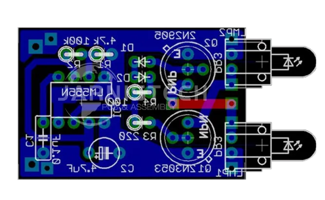
For example, in a single-layer PCB, the silkscreen typically consists of clear and concise labels like “R1” for a resistor or “U1” for a microchip, allowing the assembler to quickly identify the right component to place at the correct location. It’s this straightforward labeling that prevents costly assembly errors down the line.
| PCB Feature | Description | Common Use |
| Silkscreen Layer | Ink-based layer for labeling components | Component identification, orientation marks |
| Color Contrast | Bright, high-contrast inks like white or yellow | Ensure visibility on darker PCBs |
| Precision Printing | Ensures proper spacing and alignment | Avoid overlap, misidentification |
2.Core Functions of Silkscreen in PCB Manufacturing
Silkscreen is often seen as just a labeling tool, but it serves more than that. It helps streamline the assembly process by providing clear, standardized markings that guide assembly workers on where and how to place components on the board. These labels ensure that components go to the right spots, which results in faster assembly, fewer mistakes, and a smoother production process overall. Think of it as a helpful guide that keeps things organized, making sure everything falls into place without the confusion.
In addition, the silkscreen layer helps with PCB functionality, contributing to the overall design. It includes essential information such as component values (like resistors or capacitors), pin 1 indicators for components like ICs (integrated circuits), and even logos for branding. This makes troubleshooting, repairs, and maintenance much more efficient since technicians can easily read the printed markings on the PCB.
Take surface-mount technology (SMT) as an example: The precise placement of surface-mounted components often requires accurate positioning. A silkscreen layer provides the necessary visual guidance, ensuring components are correctly placed without any risk of misalignment or confusion.
| Silkscreen Use Case | Benefit | Example |
| Component Marking | Improves component placement accuracy | “R1” for a resistor at its designated location |
| Pin 1 Indicator for ICs | Helps prevent IC orientation errors | Indicates where pin 1 of an IC should be placed |
| Branding and Identification | Adds visual appeal and product identity | Company logo printed on the board for brand recognition |
Key Roles of PCB Silkscreen in Electronic Design
1.Facilitating Component Identification and Orientation
A major concern in PCB design and assembly is ensuring that each component is placed in the right orientation. Misplacing a component—especially a polarized one like a diode or electrolytic capacitor—can render the entire circuit inoperative. This is where silkscreen comes into play.
Through clear and legible markings on the silkscreen layer, we ensure that components are properly identified. For instance, polarized components often have a “+” sign or other distinct symbols next to them, ensuring they are oriented correctly. Without these markings, the assembly process could be delayed, and the chances of errors would be significantly higher.
2.Enhancing PCB Functionality Through Layer Management
Silkscreen also helps enhance PCB functionality by managing layers effectively, which is especially useful in multi-layer boards where visibility can be limited due to the stacked design. When the silkscreen layers are correctly printed, it prevents errors that can arise from missing or unclear markers, minimizing the chances of issues like short circuits, improper component placement, or misaligned traces. It’s like having a roadmap that guides the way, making sure every part is where it’s supposed to be and avoiding any costly mistakes down the line.
●Consider high-density interconnect (HDI) PCBs: In these designs, where components are packed tightly into smaller spaces, effective layer management becomes even more of a challenge. Here, the silkscreen serves as a guide, helping assembly technicians navigate the complexity of the design. It’s like a GPS for the assembly process, directing technicians to place components accurately, preventing mix-ups or misplaced parts. This ensures that every piece fits where it’s supposed to, even in the most intricate layouts.
| Function | Benefit | Example |
| Pin 1 and Component Orientation | Ensures correct placement of components | Pin 1 marked for ICs and diodes |
| Layer Identification | Helps distinguish between different PCB layers | Silkscreen layer marking for multi-layer PCBs |
| Component Value and Rating | Displays necessary component specifications | Resistor values, capacitor ratings |
Essential Features of PCB Silkscreen Layers
1.Ink Durability and Color Contrast
The durability of silkscreen inks is a major factor in ensuring the long-term quality of PCBs.. UV-resistant inks are commonly used to ensure that the printed text and symbols remain legible over time, even when exposed to harsh environmental conditions such as high temperatures or exposure to chemicals. These inks are formulated to withstand the stresses of the electronic environment, ensuring that component markings stay clear and readable for the lifetime of the product.
Color contrast is another feature to consider when designing silkscreen layers. The inks used in the printing process are often high contrast, such as white or yellow, to stand out against the PCB’s darker base color. This contrast ensures that the silkscreen markings are easily visible during assembly, testing, and troubleshooting.
2.Placement Precision for Improved Readability
Placement precision ensures that silkscreen layers do not overlap with areas like solder pads, traces, or vias. Proper alignment allows for clean, readable markings that don’t interfere with the functionality of the PCB.
A common issue is when silkscreen markings are printed too close to solder pads. This can lead to poor readability and, in some cases, short-circuiting or poor solder joint formation. Accurate placement ensures that the PCB silkscreen layer enhances the overall clarity without compromising the PCB’s integrity.
| Silkscreen Feature | Benefit | Example |
| UV-Resistant Ink | Ensures long-lasting legibility | Resilient text, logos, and markers on PCBs |
| High Contrast Colors | Enhances visibility and ease of identification | White or yellow ink on dark PCBs |
| Precise Placement | Avoids overlap with other important areas | Clear text and symbols without interference |
The Importance of PCB Silkscreen in PCB Manufacturing
In PCB manufacturing, the silkscreen layer does much more than just look good—it’s a core part of making sure the board functions properly and is easy to assemble. It’s more than just a pretty face—this layer of printed ink serves practical purposes, such as component identification, component orientation, and branding, among other functions. When done correctly, the silkscreen improves assembly accuracy, ensures a smooth quality control process, and gives the PCB a professional, polished look. Whether you’re assembling a simple two-layer PCB or a complex multi-layer design, the silkscreen provides the necessary markings that guide each step of production.
Enhancing PCB Assembly with Silkscreen Layers
1.Supporting Efficient Component Placement-
When it comes to PCB assembly, a major hurdle can be ensuring that all components are placed correctly. Without clear silkscreen markings, we might struggle to identify the exact location for each component. This can lead to placement errors, increased production time, and even costly rework. By utilizing precise silkscreen designs, we can make sure every component is clearly marked, improving the speed and accuracy of assembly.
For example, resistors and capacitors are often marked with their component value and position directly on the silkscreen layer. This makes it easy for us to quickly identify and place them in their designated spots. Clear silkscreen markings also help with polarized components such as diodes, which require proper orientation to function correctly. With proper PCB silkscreen placement, assembly becomes a streamlined, mistake-free process.
| Silkscreen Use Case | Benefit | Example |
| Component Placement Marks | Improves assembly speed and accuracy | Resistor “R1” and capacitor “C1” marked on PCB |
| Orientation Symbols for Polarized Components | Ensures correct positioning of components | Diode marked with a “+” sign to indicate polarity |
2.Reducing Assembly Errors Through Clear Markings-
It’s no secret that assembly errors can result in faulty products and rework that wastes both time and resources. One of the major causes of errors during the assembly process is the lack of clarity in component placement instructions. Here’s where silkscreen layers come in. With well-defined, legible markings, we can instantly understand where components go and which way they should face.
For instance, ICs (integrated circuits) have multiple pins and must be aligned in a specific direction. A well-placed pin 1 indicator on the silkscreen can save time and eliminate the risk of orientation mistakes. Silkscreen layers also make it easier for the technician to spot any potential errors in component placement early on, allowing for adjustments before soldering begins.
| Silkscreen Function | Benefit | Example |
| Clear Component Labels | Prevents misplacement of components | “U1” for IC with corresponding pin 1 orientation |
| Error Detection Early in Assembly | Minimizes risk of assembly mistakes | Early detection of missing or misplaced components |
PCB Silkscreen’s Role in Quality Control
1.Identifying Manufacturing Defects During Inspection-
PCB silkscreen layers are a fundamental part of quality control. During inspection, these layers help reveal defects such as misplaced components, misaligned parts, or even missing elements. we can use the silkscreen to cross-check the PCB layout against the design files, ensuring that everything is in its proper place before moving on to the next stage of production.
For example, a misaligned silkscreen can indicate an issue with the PCB fabrication process, such as a shift in the alignment of the copper layers or an error in the layer registration. By comparing the printed marks with the design files, quality control teams can identify and address these issues before the assembly stage, which saves both time and money.
| Inspection Use Case | Benefit | Example |
| Visual Defect Detection | Identifies misalignment or misplaced components | PCB misalignment indicated by silkscreen marks |
| Design File Comparison | Cross-checks PCB layout against the design | Comparing silkscreen layer against Gerber files |
2.Ensuring Compliance with Industry Standards-
In PCB manufacturing, sticking to industry standards is a must, and the silkscreen layers are central to meeting these standards. Whether it’s IPC-2221 for PCB design or IPC-A-600 for inspection, the silkscreen layers must follow specific guidelines, especially in areas like component labeling, marking size, and readability. These guidelines are there to ensure that the silkscreen is accurate and clear, which helps streamline both the manufacturing and inspection processes. By adhering to these standards, manufacturers can produce reliable, high-quality PCBs that meet technical and regulatory expectations.
For example, silkscreen inks must be legible at a certain size and resolution, ensuring that markings are readable even after the PCB undergoes soldering, thermal cycling, or other stress tests. Industry regulations also specify that certain components must be labeled with standard identifiers like R for resistors and C for capacitors, helping the PCB remain in compliance with manufacturing protocols.
| Standard Compliance | Benefit | Example |
| Labeling Standards | Ensures clarity and readability | Following IPC guidelines for marking component values |
| Size and Resolution Compliance | Meets industry regulations and best practices | Using appropriate font size and line thickness for silkscreen |
Aesthetic and Branding Applications of PCB Silkscreen
1.Adding Logos and Custom Labels to PCBs-
While silkscreen layers are predominantly functional, they also serve an aesthetic purpose. Many companies use the silkscreen layer to print their logo or other brand identifiers on the PCB, making the product look more polished and professional. These logos not only enhance the visual appeal of the PCB but also provide an avenue for brand recognition in the marketplace.
For instance, high-end manufacturers often print custom labels on their PCBs to indicate their brand identity, while also incorporating serial numbers or model identifiers that help track the product throughout its lifecycle.
| Aesthetic Feature | Benefit | Example |
| Branding with Logos | Adds professional and visual appeal | Company logo printed on PCBs for brand recognition |
| Custom Labels for Tracking | Enhances traceability and product lifecycle | Serial numbers or product identifiers on PCBs |
2.Multi-Color Printing for High-End Branding-
In some high-end applications, especially for premium products, manufacturers may opt for multi-color silkscreen printing. This adds a layer of sophistication and style to the PCB, allowing for a unique, eye-catching design that aligns with the overall product branding. Multi-color printing can be particularly useful when dealing with premium electronics that require a high degree of visual appeal, such as consumer electronics, medical devices, or automotive electronics.
PCB Silkscreen Design Guidelines for Optimal Layout
When it comes to designing PCB silkscreen layers, getting the layout right is not just a matter of aesthetics but also of functionality and usability. A well-designed silkscreen layout can drastically improve the assembly process, reduce errors, and even enhance the visual appeal of the PCB. Whether you’re working on a basic single-layer board or a complex multi-layer design, silkscreen layers need to be carefully planned. In this section, we’ll dive into some best practices for silkscreen placement, font choices, and how to make sure your design is optimized for readability and performance.
Best Practices for Silkscreen Placement
PCB silkscreen design isn’t just about slapping a few labels on your board—it’s about ensuring everything aligns perfectly and avoids interference with the functional layers of the PCB. Effective silkscreen placement not only boosts assembly efficiency but also minimizes the chances of defects during the manufacturing process.
1.Avoiding Overlaps with Copper Traces and Pads-
One of the primary guidelines for placing silkscreen layers is to avoid overlap with critical components like copper traces and pads. Why? If silkscreen ink is applied over a copper trace or pad, it can cause a short circuit during soldering or prevent the component lead from making a proper connection. So, you must keep clearances in mind when laying out your silkscreen marks. Best practice recommends keeping a clear zone around copper pads and traces to ensure there’s no interference.
For instance, when you’re marking resistors or capacitors on the silkscreen layer, make sure their labels or identification marks don’t overlap the copper pads where components are soldered. The extra space ensures that the ink does not contaminate the pad during manufacturing, which could cause a failure when components are soldered into place.
| Silkscreen Design Rule | Benefit | Example |
| Keep clearances between copper and silkscreen | Prevents short circuits and soldering issues | Resistor label “R1” placed away from copper pads |
| Minimize silkscreen over pads | Ensures proper component soldering | No silkscreen over a pad for IC pins |
2.Ensuring Visibility Across Layers-
When planning the silkscreen for a PCB, it’s necessary to make sure labels and markings are easy to recognize and interpret across all layers. This is especially important in multi-layer designs, where the top layer silkscreen might obscure parts of the inner layers. Proper visibility ensures that component placement, orientation, and component values are easily readable by assembly workers, inspectors, and anyone else who might need to reference the board.
To address this, we often place silkscreen markings on both the top and bottom layers of the PCB. You can also use mirrored text to ensure readability from both sides of the PCB. When designing for multiple layers, consider the silkscreen’s transparency and how it interacts with the copper layer to avoid hiding any important design features.
| Visibility Rule | Benefit | Example |
| Place silkscreen on both sides of the PCB | Maximizes readability across layers | Labeling placed on both top and bottom of the PCB |
| Use mirrored text for visibility | Ensures proper orientation across all sides | “C1” capacitor label mirrored on the bottom layer |
Managing Fonts, Line Width, and Silkscreen Readability
The design of silkscreen text—from fonts to line thickness—can significantly impact the overall readability of your PCB. After all, the ultimate goal is to ensure that any technician or engineer can easily identify components and perform assembly tasks without squinting at illegible text or unclear marks. To achieve optimal silkscreen readability, consider font sizes, line thicknesses, and contrast levels to suit the type of PCB design you’re working on.
1.Minimum Font Sizes for Clarity-
Choosing the right font size for silkscreen text is a balancing act. You want the text to be large enough to be legible, but small enough to fit within the confines of the PCB. Industry guidelines typically recommend a minimum font size of 0.8mm for alphanumeric text. Anything smaller than this can be difficult to read, especially after the PCB undergoes thermal cycling or soldering processes.
A practical example would be labeling a resistor on a PCB. The label “R1” should have a minimum font size of 0.8mm to ensure it’s readable even if the board undergoes extensive use. When dealing with smaller, more compact designs, you might opt for smaller fonts (no smaller than 0.5mm), but keep in mind that reducing font size too much could hinder readability.
| Font Size Guideline | Benefit | Example |
| 0.8mm minimum font size | Ensures text clarity and readability | “R1” on a PCB should be at least 0.8mm in height |
| Smaller fonts for compact boards | Suitable for compact designs with small components | “C1” capacitor label reduced to fit compact board size |
2.Selecting Suitable Line Thickness for Different PCB Types-
The thickness of silkscreen lines can make or break the readability of a PCB. If the lines are too thin, they could be unreadable after manufacturing due to processes like soldering, which may cause the ink to blur or spread. On the other hand, excessively thick lines can crowd out important markings or overlap components, creating confusion.
For typical single-layer PCBs, a line thickness of 0.15mm to 0.2mm is standard. However, for multi-layer PCBs, you might need to adjust the line thickness to suit the specific manufacturing requirements. In cases where high-density surface-mount devices (SMDs) are used, the line thickness should be reduced to prevent interference with the fine pitch of the components.
| Line Thickness Guideline | Benefit | Example |
| 0.15mm to 0.2mm line thickness | Ensures legibility without overcrowding | Proper line thickness for clear labels |
| Adjust thickness for high-density designs | Avoids interference with SMD components | Thinner lines in high-density designs |
Tools for PCB Silkscreen Design
Now that we’ve covered the basic guidelines, let’s look at some tools that can help you design and optimize silkscreen layers for your PCB layout. Using the right design tools ensures accuracy and efficiency, allowing you to streamline the design process and avoid errors that could lead to rework or defects.
1.Leveraging Altium Designer for Layout Optimization-
One of the top PCB design software tools in the industry is Altium Designer. Altium allows designers to seamlessly place and manipulate silkscreen layers, ensuring proper placement, alignment, and visibility. With advanced features such as design rule checks (DRC) and real-time visualization, Altium helps designers verify their silkscreen layers before moving on to manufacturing. These tools can even simulate how the silkscreen will look after various thermal and mechanical stresses, ensuring it remains intact throughout the product’s life cycle.
For instance, Altium’s 3D visualization feature lets you see exactly how your silkscreen layers will align with the rest of the PCB design, including copper traces and pads. This level of precision reduces the chances of design errors that could lead to poor manufacturability.
| Design Tool | Benefit | Example |
| Altium Designer | Advanced design rules and 3D visualization | Real-time checks for silkscreen layer overlap |
| Automatic error detection | Saves time and reduces errors | Alerts for improper font sizes or line thicknesses |
2.Using Cadence for Precision Silkscreen Layer Design-
Another popular design tool for PCB silkscreen is Cadence PCB Editor. Cadence offers precision tools that help you adjust every aspect of your silkscreen layer for optimal clarity and performance. The software provides various options for silkscreen layering and allows for integration with the Gerber file generation process, ensuring a smooth transition from design to production.
With Cadence, we can create silkscreen layers that match perfectly with the PCB’s copper layers. This tool also offers automated alignment checks and rule enforcement to ensure that your silkscreen does not interfere with functional layers or cause issues in the manufacturing process.
| Design Tool | Benefit | Example |
| Cadence PCB Editor | Precise layer design and rule enforcement | Alignment checks for silkscreen layer accuracy |
| Gerber file integration | Seamless transition from design to production | Cadence helps in generating precise Gerber files for silkscreen layers |
Common PCB Silkscreen Printing Methods and Techniques
PCB silkscreen printing isn’t just about getting your labels onto a board—it’s about precision, efficiency, and ensuring your boards are easy to assemble and debug. The method you choose can influence the quality of your final product, the cost-effectiveness of the production, and how fast you can get it to market. Let’s break down some of the common techniques used in PCB silkscreen printing today.
Manual vs. Automated Silkscreen Printing
1.Manual Printing: Comparing Efficiency and Accuracy-
Let’s be real—manual PCB silkscreen printing is something of a blast from the past. But, it’s still relevant, especially for small runs or for prototyping. In manual printing, the operator uses a stencil to apply ink to the PCB. This method requires skilled labor to maintain accuracy and consistency, and while it works well for low-volume runs, it’s far less efficient for larger batches.
●Efficiency: Think of manual printing like handcrafting something—you get a personal touch, but it takes longer. This method can also be prone to human error. For small-scale production, it’s a good option because the setup costs are relatively low, but once you get into higher quantities, automation tends to win.
●Accuracy: On the other hand, manual silkscreen printing has a bit more flexibility for customizing the silkscreen on the fly, but it still depends heavily on the technician’s skill to ensure consistent, accurate placement of the silkscreen on each PCB.
| Criteria | Manual Printing | Automated Printing |
| Setup Cost | Low | High |
| Speed | Slower | Faster |
| Precision | Dependent on skill | High and consistent |
| Suitable for | Prototypes, low volume | High-volume production |
| Labor Costs | High (operator skill needed) | Low (minimal human intervention) |
2.Automated Printing: Boosting Speed and Consistency-
Automated silkscreen printing is the modern way to go, especially if you’re looking at higher volumes. This method uses machines to apply the silkscreen ink, making it much faster and more precise than manual printing. For high-volume production runs, automation provides both speed and accuracy that manual processes just can’t match.
●Efficiency: Automated processes are lightning-fast, with minimal downtime. The machines can run continuously with little human interaction, which makes them much more efficient for mass production. Plus, the consistency is spot-on for every board—this eliminates a lot of the guesswork that comes with manual methods.
●Accuracy: When it comes to precise placement of silkscreen on multi-layered PCBs, automated printing is where you’ll want to be. The machines are designed to handle complex designs, so you get accurate, consistent markings every time.
How Printing Silkscreen on PCB?
The process of printing screen is the process of stretching fine stainless steel or polyester wires on a rigid frame that acts as a carrier for images. The stencil for the desired image is made using photosensitive glue onto the mesh. The emulsion is typically applied to each side of the mesh, and a specified thickness is constructed on the side that is under (the part that touches the boards).
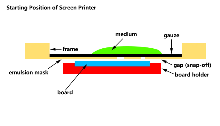
As illustrated in the figure as shown in the figure, the screen is placed right above the board as well as the medium (ink) is placed behind an elastic squeegee. As the squeegee is moving across the screen and the mesh of the screen gets into proximity to the PCB and allows the medium to flow across the PCB.
The squeegee blade is initially pressed into the openings of the image. Then, it removes excess material when it moves over each of the apertures. The mesh aperture on the screen gets separated from the print surface by the squeegee leaving the ink behind that was within an aperture in the mesh. The medium moves in a slight manner after printing to minimize visible mesh marks that are left on the print. This process is known as leveling.
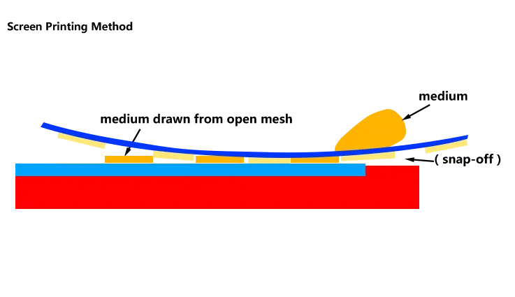
Since the screen is in contact with the substrate as the squeegee is able to pass across it, this method is often referred to in the field of off-contact printing. For every 100mm of the frame’s width, the snap-off distance typically is 0.5mm. Its thickness ink will be determined by the amount of emulsion, as well as the mesh.
Advanced Printing Techniques for PCB Silkscreen
Sometimes, you need to step it up and go beyond the basics to ensure your PCB silkscreen layers have the kind of quality that grabs attention. That’s where advanced silkscreen printing techniques come into play. These techniques are designed to handle more complex designs, including multi-color printing and high-precision applications.
1.Multi-Color Silkscreen Printing: Aesthetic and Functional Appeal-
When you’re designing PCBs that require multiple silkscreen colors, it’s no longer just about functionality. Multi-color printing adds another layer of aesthetic appeal and brand identity to your product. Whether you’re aiming for a clean, professional look or need more clarity in component identification, multi-color silkscreen printing opens up a world of possibilities.
●Applications: Think of multi-color silkscreen printing as your secret weapon for high-end electronics. For example, smartphones, wearable devices, and consumer electronics often incorporate multi-colored silkscreen layers to indicate different components, directions, or even special features. Brand logos and custom designs are printed in vivid colors, adding a professional touch to your board.
●Precision and Quality: The latest in multi-color printing tech can handle complex designs with high resolution and precise alignment. This is key for boards that need both clarity and durability.
Advanced Printing Techniques:
| Technique | Description | Applications |
| Multi-Color Printing | Multiple ink layers for visual clarity and branding | Consumer electronics, high-end products |
| High-Precision Printing | Use of fine-mesh screens for tighter ink application | Medical devices, aerospace |
| UV curing | Drying method for fast curing of the ink | Flexible PCBs, high-density boards |
2.Innovations in High-Precision Printing Methods-
Advances in silkscreen printing technology have brought a new level of precision to PCB production. High-tech tools like laser printers and direct-to-board systems can handle the intricate demands of modern designs with ease, especially for applications like high-density interconnects (HDI) and fine-pitch PCBs. Laser systems, in particular, are like the sharpest tool in the shed when it comes to creating detailed and accurate markings. This precision ensures every label is spot-on, reducing the risk of mix-ups during assembly and inspection. With these innovations, we can hit the ground running, tackling even the most challenging layouts without breaking a sweat.
Materials and Equipment for PCB Silkscreen Printing
The choice of materials and equipment you use for silkscreen printing will heavily influence the durability and quality of the final product. Let’s take a look at some of the top-tier inks and equipment available for this purpose.
1.High-Quality Inks for Durable Silkscreen Layers-
When choosing inks for PCB silkscreen printing, you need to think about durability and adhesion. Epoxy-based inks are commonly used for high-performance applications due to their strength and longevity. They bond well with the PCB surface and resist fading or damage over time, even in harsh environments.
Types of Inks:
| Ink Type | Features | Best Use Cases |
| Epoxy-based inks | Strong adhesion, durable, and heat-resistant | High-end electronics, automotive |
| UV-curable inks | Cures quickly under UV light, fast production | High-speed assembly lines |
| Solvent-based inks | Flexible, suitable for flexible PCB applications | Flexible PCBs, wearable tech |
2.Equipment for Achieving Consistent Results-
The tools you use for silkscreen printing also play a crucial role in the outcome. Whether you’re using manual screen printing equipment or investing in automated silkscreen printing machines, you’ll need the right tools for the job.
For high-precision silkscreen printing, it’s worth investing in advanced machines that offer fine control over ink deposition, alignment, and layer consistency. These machines can apply multi-color inks with high accuracy, ensuring the labels and markers are consistently aligned across all PCBs.
| Equipment Type | Features | Applications |
| Manual Screen Printing | Lower cost, ideal for low-volume runs | Prototyping, small-scale production |
| Automated Silkscreen Printers | High-speed, precise alignment, multi-color capabilities | High-volume production |
| Laser Direct Printing | High precision, capable of fine-line printing | High-density boards, medical devices |
Challenges and Solutions in PCB Silkscreen Processes
When it comes to PCB silkscreen, the process is not without its challenges. From printing defects to design limitations, we often face obstacles that can affect the quality and readability of the silkscreen layer. However, with a clear understanding of common issues and proactive solutions, these challenges can be overcome. In this section, we’ll dive into the troubleshooting process, address design limitations, and explore the redesigning of silkscreen layers.
Troubleshooting Common Silkscreen Issues
Silkscreen printing is a delicate process that requires precision, but sometimes things go wrong. Whether you’re dealing with misalignment or ink smudges, these issues can negatively impact the final product. Identifying and fixing these common issues quickly helps maintain efficiency and ensures the highest standards are met. By addressing these challenges effectively, we can keep their processes running smoothly and uphold product quality.
1.Identifying and Resolving Printing Defects-
Printing defects such as incorrect ink coverage or poor resolution can cause a lot of frustration in PCB production. The first step in troubleshooting is identifying the source of the problem. For example, if the silkscreen layer appears blurry or inconsistent, it could be a result of improper exposure to the UV light during the stencil process or contaminated screens. Another possible culprit is the screen tension—if the tension is too loose, the ink may spread unevenly, leading to fuzzy prints.
●Solution: If you’re seeing defects, start by inspecting the stencil quality and ensuring the screen mesh is free from dust and contamination. It’s also important to make sure the ink viscosity is correct; too thick, and the ink won’t flow properly; too thin, and it won’t provide the needed opacity. Keep your printing equipment well-maintained and regularly calibrated to avoid most common printing defects.
2.Addressing Ink Smudges and Misalignments-
Another common issue in PCB silkscreen printing is ink smudges and misalignments. This can happen if the screen mesh isn’t properly aligned with the PCB during the printing process. It may also occur if the ink layer is too thick, causing excess ink to spread beyond its intended area, leading to smudges.
●Solution: The key to avoiding smudges is using the right amount of ink pressure and ensuring proper registration alignment. Regular calibration of your printing equipment can also help ensure that the silkscreen is applied precisely where it needs to go. Furthermore, using laser alignment systems can significantly improve the accuracy and consistency of your printing.
Example: In high-density PCB designs, where the silkscreen must fit within tight tolerances, any misalignment or smudge could compromise the clarity of component labels or traces. By incorporating automated registration systems, we can ensure that the silkscreen layer aligns perfectly with the underlying copper traces and pads.
Overcoming Design Limitations in PCB Silkscreen
PCB silkscreen printing comes with its own set of design limitations. Whether it’s space constraints on high-density boards or the challenge of balancing aesthetic appeal with functional requirements, addressing these limitations is first step to ensuring a successful design.
1.Ensuring Readability in High-Density PCBs-
With high-density PCBs, the amount of available space for the silkscreen layer becomes limited. Micro vias, fine-pitch components, and small pads all make it difficult to print readable text and symbols. As PCB designs get smaller and more complex, the silkscreen layer must be carefully crafted to ensure legibility without taking up too much space.
●Solution: One solution is to use fine-line printing techniques, which allow for smaller fonts and detailed symbols to be printed clearly, even in tight spaces. It’s also worth considering multi-layer silkscreen applications, where the silkscreen is distributed over multiple layers to manage space more effectively.
2.Balancing Aesthetic and Functional Requirements-
When designing a PCB, functional labeling like part numbers and polarity markers are essential, but let’s not forget the look of the board. Adding multi-color printing can make your PCB pop and look more polished, but it also comes with a higher price tag and may complicate the manufacturing process. The trick is to find that sweet spot between functional clarity and aesthetic appeal.
●Solution: It’s a smart move to set your design priorities from the get-go. In some cases, a monochrome silkscreen might be sufficient, allowing for faster and more cost-effective production. However, if branding is a significant part of the product, multi-color and customized silkscreen designs can add value to the final product, enhancing both appearance and brand identity.
Example of Aesthetic vs. Functional Balance:
| Design Element | Functionality | Aesthetic Impact |
| Text Labels | Easy identification of components | Monochrome silkscreen is typically sufficient |
| Branding Logos | Custom labels for brand recognition | Multi-color printing adds value and appeal |
| Warnings & Indicators | Polarity, test points, and safety marks | Minimal design required for clarity |
Removing and Redesigning PCB Silkscreen Layers
Sometimes, silkscreen layers need to be removed or redesigned due to defects or design changes. Whether it’s to fix a printing error or update the PCB for a new version of a product, it’s necessary to approach silkscreen removal with care.
1.Safe Removal Techniques for Faulty Silkscreen-
Removing a faulty silkscreen layer requires precise techniques to avoid damaging the PCB. Abrasive methods, such as sanding or scraping, can cause board damage. Instead, use chemical solvents designed specifically for silkscreen removal, ensuring that the circuit traces and pads remain intact.
●Solution: Start by testing a small area of the silkscreen with a non-abrasive solvent. Use a soft brush to gently remove the layer without affecting the underlying copper traces. If you’re working with a reworkable PCB, make sure to verify that all silkscreen marks are cleanly removed before applying new designs.
2.Implementing Redesigns to Enhance Future PCBs-
After identifying issues with the original silkscreen design, you may need to redesign the layout for future PCB versions. This could involve adjusting font sizes, re-aligning component markers, or redesigning the color scheme to improve readability or branding. To ensure that these redesigns meet quality standards, it’s necessary to simulate the changes using PCB design software before committing to a new production run.
●Solution: Use simulation tools to test how the redesigned silkscreen will appear on the actual PCB. This allows us to visualize potential issues and make adjustments before the design is finalized for production. Additionally, implementing automated inspection systems can help catch design flaws early in the process.
Top PCB Manufacturer in China – JarnisTech!
With more than 20 years of experience as a market-leading company, JarnisTech is one of the most professional PCB manufacturer in China. Highly specialized not just in the development of prototype PCBs and PCB assembly but also in small and medium-sized quantity PCB fabrication. We can silkscreen your PCBs, and we’ll do our best to meet the requirements of silkscreen.
Why Choose US:
1.Extensive Experience in PCB Manufacturing
We know that PCB silkscreen isn’t just about aesthetics—it’s an integral part of your board’s functionality and identification. From component markings to debugging points, our silkscreen solutions help streamline your production process, making assembly faster and reducing errors.With JarnisTech, you can trust that every silkscreen layer is applied with precision. Our team utilizes the latest in automated silkscreen printing techniques alongside tried-and-true methods, ensuring accuracy and speed.
2.Tailored Solutions for Your Unique Needs
We understand that every project is unique. Whether you need high-contrast silkscreen markings for component identification, branding with custom logos, or specialized inks for harsh environments, we’ve got you covered. We provide a variety of silkscreen colors, including white, yellow, and black, ensuring that your board looks professional and functions flawlessly.
Our design team will work closely with you to meet the specific requirements of your design. We know that every line, every text, and every color matters. With our years of expertise in PCB silkscreen design, we ensure your PCB will meet the highest standards, whether for aesthetic branding or clear, readable functional marks.
3.Why Silkscreen Matters in PCB Manufacturing
Precision and Durability: PCB silkscreen is about more than just marking; it’s about ensuring that the markings are visible, legible, and long-lasting. We use high-quality inks and advanced printing techniques to ensure that your silkscreen layer stands up to the rigors of soldering and other PCB manufacturing processes.
Our’s PCB Print Service:
| Items | Competencies |
| Silkscreen Colour | Black,White, Yellow |
| Solder Silkscreen Brand | KSM-388 white/black, Taiyo S-380W white, ATA-5000 yellow |
| Silkscreen Line Width | 5mil |
| Silkscreen Text Height | 27mil |
| Character Printer (Only White) | Serial, Bar Code, QR Code |
| Silkscreen to Solder Pad Space | 6mil |
Should you need to ask about any concerns you have, feel free to reach us via [email protected]. We’ll be glad to assist you.
FAQs related to PCB Silkscreen:
What’s the difference between silkscreen and soldermask on a PCB?
Silkscreen is used for labels and markings, while soldermask protects copper traces and prevents solder bridges.
How does silkscreen affect PCB durability?
Silkscreen ink must be durable to withstand heat and soldering processes, affecting the longevity of markings.
What challenges does silkscreening pose on flexible PCBs?
Flexible PCBs require special inks and application techniques to prevent cracking or peeling due to their bendable nature.
Can silkscreen be used for debugging and test points?
Yes, silkscreen marks test points and pads for easier troubleshooting and testing.
How does silkscreen design impact PCB assembly time?
Clear silkscreen markings speed up assembly by guiding component placement and reducing errors.
What factors should be considered when choosing silkscreen colors?
Contrast and visibility are key, with white for clarity and yellow often used for high-end or aesthetic purposes.
Can multi-layer PCBs have silkscreen on all layers?
Typically, silkscreen is applied to outer layers, but inner layers may have it for specific purposes.
What environmental concerns exist with silkscreen inks?
Some silkscreen inks contain harmful chemicals, but eco-friendly inks are available to meet environmental standards.


