
An effective SMD Solder Paste Stencil is critical to the success of a Precision electrical PCB assembly because it is used to apply the correct solder paste (also known as tin cream) to the bare printed circuit boards in order to create the necessary electrical connections. JarnisTech began offering Laser Stencils as a means of ensuring the quality of your PCB assemblies in order to satisfy the growing demand for higher part densities and more compact components in PCB assemblies.
All of JarnisTech’s stencils are completely cut by laser, and they are made of 304 stainless steel with extremely smooth windows that allow for the most effective release of solder paste. JarnisTech is a manufacturer of PCBs and assemblies. The provision of frameless and framed SMD stencils in a range of sizes is made available with the intention of meeting all solder paste printer and stencil requirements.
PCB assemblers who have experience know that the amount of solder paste that is printed on the circuit boards can be controlled by the thickness of the stencil foil and the size of the aperture joint. An insufficient solder joint is caused when there is not enough paste. Solder can form solder balls, bridges, and tombstones when there is an excessive amount of paste.
What Is PCB SMD Stencil ?
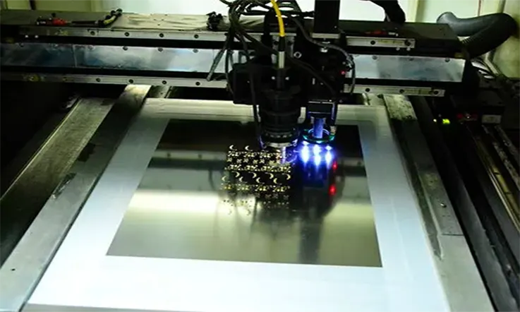
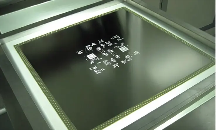
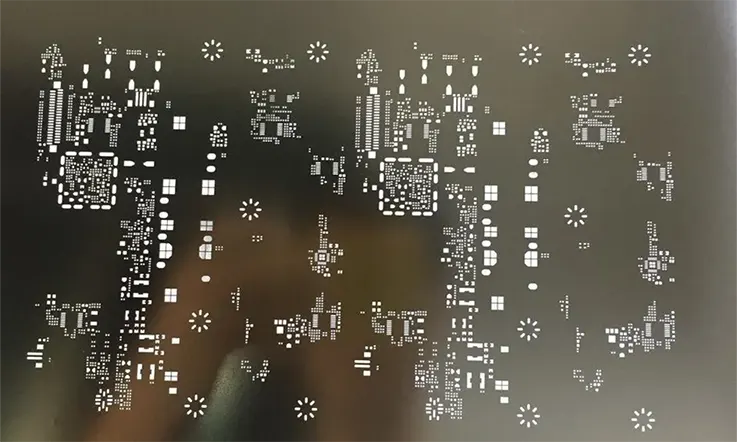
An SMT stencil’s main purpose is to transfer solder paste to a bare circuit board. A stainless steel foil is laser-cut to create a hole for each surface-mount component on the circuit board. Once the stencil is aligned appropriately on the circuit board, solder paste is applied to the openings (making a single pass, using a metal squeegee blade). When the stainless steel foil is detached from the circuit board, the solder paste will be exposed and ready for SMD installation. As opposed to soldering by hand, this procedure maintains consistency and saves time.
Main features:
● Reduce circuit board assembly time.
● Enhance the quality of your circuit board prototypes.
● Reduce the time-consuming and error-prone procedure of manually soldering circuit boards.
PCB Stencil Design Tips
Printing your stencil design is the essential first step to take if you want to acquire flawless and dependable solder junctions. The thickness of the pad stencil has a one-to-one correspondence with the size of the openings in the pad stencil that surround it. In general, thicker stencils can be produced with an opening that is somewhat smaller than the pad size, while the opening size of thinner stencils can be designed 1:1. While making a steel mesh with openings, the employment of a laser in conjunction with electropolishing is strongly encouraged.
PCB Stencils Design: Surrounding Pads
The amount of solder paste that gets printed onto the PCB is directly proportional to the thickness of the stencil. During the reflow soldering process, bridging will occur if there is an excessive amount of solder paste. Because of this, it is suggested that the 0.5mm pitch QFN package utilize a steel mesh that is 0.12mm thick, while the 0.65mm pitch QFN package utilize a steel mesh that is 0.15mm thick. In order to cut down on the amount of solder that bridges across pads, the opening in the stencil can have a size that is proportionately smaller than that of the pad.
PCB Stencil Design: Heat Dissipation Pad
When the exposed pads on the bottom of the chip are soldered to the thermal pads on the PCB, the gas that is contained within the thermal vias and large-size pads will overflow and create certain air holes. This happens because the gas cannot escape through the thermal vias and large-size pads. Hence, if the area of the solder paste is too large, it will generate a number of different faults (such as sputtering and solder balls, etc.). Unfortunately, it is only possible to reduce the size of these pores; it is not possible to completely get rid of them. When developing the stencil for the region of the thermal pad, considerable thought needs to be given.
Instead of a single enormous aperture, it is suggested to make numerous smaller openings in this location. 50% to 80% solder paste coverage is the normal range. In practice, it has been demonstrated that a solder joint thickness of 50m is quite beneficial for enhancing board-level reliability. In order to reach this thickness, it is recommended that the solder paste thickness for the underfill thermal via design be at least 50% and the coverage rate for the through hole be at least 75%.
Accuracy of SMD Stencil
Each and every one of JarnisTech’s laser cut stainless steel stencils goes through the exact same production process, ensuring that they all have the same level of precision. The accurate laser cut, which has a blade clearance of only 20µm, is the determining factor in our product’s excellence.
Our SMD-Stencils meet the strictest quality standards with excellent register accuracy and cutting precision. The exact axial tolerance of ± 2µm and repetition precision of ± 3µm provide ideal conditions for solder paste printing, even for the smallest high-tech components.
Moreover, laser-cut stencils include pads with a slight conical hole on the side facing the circuit board, which gives the solder paste the best possible release behavior.
Where Is PCB Laser Cut SMD Stencil Manufactured ?
In manufacturing rooms equipped with air conditioning and fiber lasers, stainless steel stencils that have been cut by laser are made. Reduced heat input is possible thanks to the lower cutting opening, which is now 20µm rather than the previous 40µm. The depth of focus sharpness remains the same. At the same time, the edges have become smoother, and the laser cutting of the stainless steel stencils is more accurate.
The accuracy provided by the apertures with a lightly conical shape enables a more effective release of the solder paste and expands the process window for the pick-and-place operation. It is vital for the process of laser cutting to take place in constrained conditions in order to generate laser cut stainless steel stencils that are accurate to their intended size.
If your PCB manufacturing company can produce stencils, they can also produce stencils for you. For panel fabrication, a Gerber file is essential. If you wish to construct your own PCB stencil, make sure you ask them to create the corresponding GBC file.
Types Of High Quality SMD Stencils
Framed SMD Stencils
Framed SMT stencils, also known as “glue-in” stencils, are laser-cut solder paste stencils that have been permanently mounted in a stencil frame. The stencil frame has a mesh border that is used to stretch the stencil foil as taut as possible within the frame. Screen printing on printed circuit boards can be done in huge volumes with framed stencils due to their design. Framed SMD stencils provide smooth aperture walls and are appropriate for usage with pitches of 16 mils or less as well as micro BGAs.
Features:
● Excellent print performance.
● 24-hour turnaround standard.
● Very clean laser-cut apertures.
● Unique Process for smooth aperture walls.
● All framed SMD stencils are double bonded to extreme wear.
● Excellent for high-volume stencil printing on printed circuit boards.
● Unique approach creates permanent non-removable non-fading fiducial.
Frameless SMD Stencils
Frameless SMD Foils, sometimes known as stencils, are laser-cut solder paste stencils designed to function with stencil tensioning devices called reusable stencil frames. This form of stencil does not require permanent affixation to a frame. Frameless stencils are much less expensive than framed stencils and offer cost-effective storage while yet maintaining outstanding performance and quality.
Features:
● 24-hour turnaround standard.
● Reduced storage space requirements.
● Significantly less expensive than framed stencils.
● Excellent for prototype printed circuit board assembly or short runs.
● Smooth aperture walls, usable for 16 mil pitch or less and Micro BGAs.
Prototype SMD Stencils
Prototype surface-mount device (SMD) stencils are laser-cut stencils that are manufactured to order from the PCB Gerber files or CAD files you provide in order to precisely match your prototype printed circuit board. These frameless solder paste stencils are made with the sole purpose of being used for hand printing.
Features:
● 24-hour turnaround standard.
● Lower cost than production stencil.
● Reduce PCB prototype assembly time.
● Includes complete “how-to” instructions.
● Improve quality of your prototype printed circuit boards.
● Reduce the time-consuming and error-prone procedure of manually soldering prototype circuit boards.
Electroformed SMD Stencils
Electroformed SMD stencils are nickel-based electroform foils that are permanently placed in a stencil frame using a mesh border to securely stretch the stencil foil taut in the frame. These stencils are also known as electroformed nickel stencils. Electroformed stencils are widely used for fine pitch SMT applications on printed circuit boards, which range from 20 mil to 12 mil in pitch. These stencils give the best paste release properties that are currently available. In addition to that, BGAs, flip chips, and wafer bumping are all possible applications for them (12 mil to 6 mil pitch).
Features:
● 24-hour turnaround standard.
● Nickel has a lower coefficient of friction compared to stainless steel.
● The electroformed stencil’s smooth trapezoidal sides facilitate paste release.
● Electroform foils have a higher hardness than full hard stainless steel of a corresponding thickness, and provide a longer stencil life.
SMD Stencil Capabilities
| Material | Foil: 304 stainless steel and nickel-based Frame: Aluminum |
| Stencil Size | 370x470mm [14.5’’x18.5’’];420x520mm [16.5’’x20.5’’]; 550x650mm [22.0’’x25.5’’];735x735mm [29.0’’x29.0’’] Other size can be customized. Long 1600mm SMT Stencil can be provided. |
| Stencil Type | SMT Stencil [Framed SMT Stencil] SMT Stencil Foil [Frameless SMT Stencil] |
| SS Foil Thickness | 0.10mm (4mil);0.12mm (5mil);0.13mm (6mil); 0.15mm (7mil);0.18mm (8mil);0.20mm (10mil) |
How to clean an SMD Stencil
In most cases, professional cleaning equipment is utilized in order to clean SMT stencils. The smart stencil cleaning machine is now the most popular product on the market. This machine is designed for use in the electronic sector and is intended for cleaning SMT stencils, copper stencils, wire stencils, microporous stencils, and wafer trays. The apparatus employs compressed air as its source of energy; it does not require electricity; it does not pose a risk of fire; it cleans stencils comparable to those used in manufacturing.
It employs high-performance automated air pressure operation and a user-friendly, one-button interface to facilitate the completion of cleaning and drying activities. As for equipment cleaning, the cleaning fluid is recycled with minimal loss.
Summary
Printed Circuit Board Design Services and Capabilities
We have made it our mission to become a highly dependable multi-layer board manufacturer, and to that end, we have made substantial investments in the development of a PCB industrial park that spans an area of 136,888 square meters and meets stringent international environmental protection qualifications. Therefore, we can provide one stop service for PCB manufacturing and Assembly to our clients. If you wan to learn more about printed circuit boards capabilities, please visit our PCB Product Comparison as well as our Circuit Board Assembly & Manufacturing Capabilities pages for additional information regarding how we can be of assistance to your company.


