
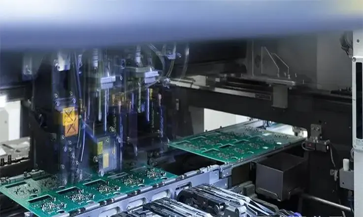
PCBA (Printed Circuit Board Assembly) depaneling is the process of separating individual PCBs from a larger panel or array. This is necessary when manufacturing or assembling electronic devices that require small or customized PCBs. Depaneling can be done using a variety of methods, such as milling, routing, laser cutting, or mechanical punching, depending on the PCB design and the required precision.
A PCBA depaneling carrier is a specialized tool that helps to securely hold the PCB during the depaneling process. The carrier provides a flat and stable surface for the PCB and prevents it from distorting during cutting. It also protects the PCB from damage and prevents the components from falling off or getting dislodged during cutting.
The need for a PCBA depaneling carrier arises from the increasing trend towards smaller and more complex electronic products that require highly customized PCBs. Without a carrier, the depaneling process can be time-consuming, error-prone, and can lead to damage or defects in the PCB or components. The carrier simplifies the process, reduces the risk of damage, and ensures consistent and accurate cuts.
What Is PCBA Depaneling ?
In the high-volume production of electronic assemblies, an important process step is known as depaneling. Printed circuit boards (PCBs) are often designed with a large number of smaller individual boards, referred to as a panel or multiblock, in order to enhance overall production capacity for manufacturers of PCBs and surface mount technology (SMT) lines.
At a particular stage in the production process, this collection of PCBs, or panel/multiblock, is disassembled, a process known as “depaneling.” The exact timing of this stage varies depending on the type of product being manufactured. It may occur immediately after the SMT process, after the in-circuit test (ICT), after the soldering of through-hole elements, or even immediately prior to the final assembly of the printed circuit board assembly (PCBA) into the enclosure. This step in the production process allows for efficient and effective assembly of high-quality electronic products.
PCBA Depaneling Methods
There are several methods for PCBA depaneling, each with its own strengths and limitations. Here’s an overview of the most common methods:
● Milling: This method uses a cutting tool to remove the PCB material along the designated cutting path. Milling is precise and can handle complex shapes, but it generates more dust and debris than other methods and tends to be slower.
● Routing: This method uses a router tool to remove the PCB material along the cutting path, typically in a straight line. Routing can be faster than milling, but it may struggle with intricate or curved shapes, and it generates more vibration.
● Laser cutting: This method uses a laser beam to cut through the PCB material along the designated path. Laser cutting is highly precise, fast, and can handle intricate shapes, but it requires specialized equipment and can generate heat and smoke, which can damage the components or the PCB itself.
● Mechanical punching: This method uses a punch tool to create a hole or a slot along the designated path. Mechanical punching is fast, but it may damage the PCB if there is insufficient clearance between the tool and the components.
● V-scoring: This method creates a groove or a V-shaped notch along the designated cutting line, which weakens the PCB and allows it to be snapped apart manually. V-scoring is fast, cost-effective, and suitable for high-volume production, but it may have limited accuracy and may not work well for more intricate shapes.
As a result, the choice of PCBA depaneling method depends on the PCB design and the required precision, speed, and cost-effectiveness. Some methods may also require the use of a depaneling carrier to securely hold the PCB during cutting.
PCBA Depaneling Carrier
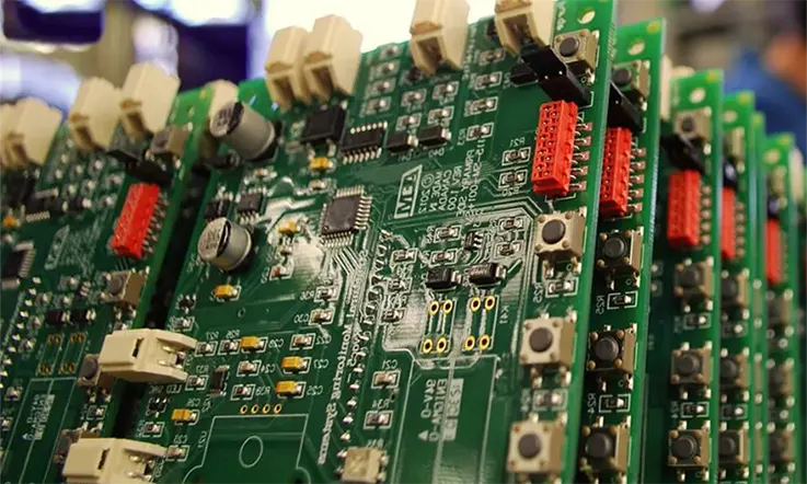
Printed Circuit Boards, or PCBs, are typically produced in large panel configurations known as Depaneling Carriers, containing several boards simultaneously. However, they can also be manufactured as individual pieces depending on market requirements. After completing the assembly and ensuring all necessary checks are conducted on the PCBA panels, it is time to proceed with the depaneling process.
It is important to note that the depaneling method employed by your contract manufacturer can significantly affect the cost and quality of your PCB assembly, particularly when developing compact electronic products. Typically, PCBs are less than 100 millimeters (39.37 mil) in width and are separated, or “depaneled,” into individual boards following assembly.
To avoid potential issues and reduce expenses, it is vital for you and your designers to understand the available depaneling methods and consult with your contract manufacturer before finalizing any PCB design. Proper planning and communication during this stage can help ensure the success of your PCB assembly project.
When selecting a depaneling method, it is essential to take into account the risks involved. These risks may include:
● Tolerance: During the depaneling process, certain methods may result in a printed circuit board assembly (PCBA) with dimensions that differ from the intended size. In order to minimize this risk, it is prudent to communicate closely with the manufacturer regarding which measurements are most critical. Additionally, selecting a depaneling method tailored to your specific requirements can be helpful.
It should be noted that manual depaneling will typically have the most lenient tolerance, while laser depaneling will have the most stringent. By understanding the unique qualities of each depaneling method and selecting the most appropriate one, you can help ensure that your PCB assembly satisfies the required specifications and standards.
● Mechanical Strain: Depaneling can exert significant force that may cause the printed circuit board (PCB) to bend, potentially damaging components or causing trace fractures in the worst-case scenario. To minimize this risk, it is advisable to avoid placing components too close to the edge of the printed circuit board assembly (PCBA), and to ensure proper alignment of components so that they are parallel to the break line.
By strategically positioning components and proactively considering the potential effects of depaneling on the PCBA, you can help reduce the likelihood of damage and ensure a high-quality final product. Maintaining constant communication with your contract manufacturer can also help to identify and address potential issues during the depaneling process.
The Choice of Depaneling Method Can Impact Various Factors, Including:
● Tolerances: Selecting a printed circuit board (PCB) manufacturer with laser cutting capabilities is recommended when working with PCB designs that have very tight tolerances or require components to be placed in close proximity to the board’s edge. The precision and versatility of laser cutting technology make it an ideal choice for PCB fabrication in such cases.
By selecting a manufacturer with the appropriate equipment and expertise, designers and engineers can ensure that their PCB assemblies are precise, reliable, and meet the required specifications. Careful consideration of the specific needs of each project can help to ensure a successful outcome and minimize the potential for costly errors or delays.
● Tooling Costs: Depaneling with punches may require customized tooling to accommodate the specific layout of the PCB. In contrast, programmable laser cutting devices typically have a shorter setup time. The use of cutters may or may not necessitate specialized tools, depending on the specific requirements of the task.
For large-scale production of flexible circuits, a combination of punching and laser cutting is often necessary to achieve the desired results. Careful consideration of the unique characteristics of each depaneling method can help to ensure efficient and reliable production of high-quality PCB assemblies. By leveraging the strengths of each technique, designers and engineers can achieve optimal results for their specific application requirements.
● Labor Cost and Throughput: In comparison to laser cutting, manual depaneling techniques such as cutting and punching are typically faster. Examples of manual operations include the use of cutters and punches. However, if sanding of the edges is needed, additional time and costs will be incurred.
When choosing a depaneling method, it is important to balance factors such as speed, cost, and final product quality in order to arrive at the most optimal solution for the specific project or application. By leveraging the unique strengths of each depaneling technique, manufacturers can ensure the efficient production and reliable performance of their PCB assemblies.
● Material Cost: Maximizing the number of circuit boards within a traditional PCB panel can help to reduce waste and material costs. PCB designers can carefully craft both the layout and array drawings, taking into account the limitations of the depaneling process.
During the surface mount device (SMD) assembly, it is important to maintain a safe distance between the components and the edges of the board to prevent damage from depaneling tools. In cases where engineers are uncertain about the specific tools that will be employed, it may be prudent to err on the side of caution by creating a PCB that is slightly larger than strictly necessary for the depaneling carrier.
By closely monitoring these factors and taking proactive measures to anticipate potential issues, designers and engineers can help to ensure that the PCB assembly process proceeds smoothly and efficiently while maintaining the high quality of the finished product.
Types of PCBA Depaneling Carriers and Their Features
There are several types of PCBA depaneling carriers, each with its own features and benefits. Here’s an overview of the most common types:
● Magnetic carriers: These carriers use powerful magnets to securely hold the PCB during cutting. Magnetic carriers are easy to use, require minimal setup time, and are suitable for a range of PCB sizes and shapes. One downside is that they may not be suitable for all types of cutting methods, such as laser cutting, which requires nonmetallic carriers.
● Vacuum carriers: These carriers use suction to hold the PCB in place during cutting. Vacuum carriers are versatile and can accommodate different PCB sizes and shapes, but they require a clean and dry environment to work effectively. They are more suitable for smaller and lighter boards compared to larger and heavier ones.
● Mechanical carriers: These carriers use a mechanical clamping or gripping mechanism to hold the PCB in place during cutting. Mechanical carriers are suitable for larger and heavier boards than magnetic or vacuum carriers and are less prone to vibration and distortion. They may require more setup time and adjustment and may be less suitable for irregularly-shaped boards.
● Rigid fixtures: These carriers use a rigid fixture or frame to hold the PCB in place during cutting. Rigid fixtures offer excellent stability and precision, making them suitable for very large or irregularly-shaped PCBs or more demanding cutting methods. They may be more expensive, however, and require more setup time and maintenance.
● Flexible fixtures: These carriers use a flexible or conformal fixture to hold the PCB in place during cutting. Flexible fixtures can be customized to fit irregularly-shaped or curved PCBs, making them suitable for more complex cutting methods. They are also typically less expensive than rigid fixtures, but may require more setup time and maintenance.
So, the choice of PCBA depaneling carrier depends on several factors, including the PCB design and size, the cutting method used, the desired precision and stability, and the available budget and resources.
How Many Types PCBA Depaneling Technology ?
● Laser Cutting: Laser cutting is a contemporary technique utilized for depaneling that effectively eradicates bending forces. This method involves the use of a laser to make highly precise and minute incisions in various designs of flexible PCB assemblies. Laser cutting empowers placement of components extremely close to the board’s edge, enabling optimal utilization of board area in small and compact PCB assemblies.
● Cutter: Printed circuit board (PCB) panels are usually fabricated with v-scores between each board, particularly when the printed boards are rectangular in shape. Once the components have been installed and soldered onto the boards, we utilize specialized equipment to separate them along the scored lines in a manner that minimizes bending stress. Thinner boards can be sliced by a guillotine-like cutter, whereas larger boards necessitate the use of a wheel cutter commonly referred to as a “pizza cutter.”
● Router with Dust-proof: To achieve the depanelization of curves and other intricate shapes of printed circuit boards (PCBs), some PCB assembly manufacturers utilize a mechanical router. This method reduces bending stress but simultaneously increases vibration stress. Additionally, a significant amount of dust is generated during the routing process, necessitating the use of a dust-proof router by a professional PCB assembly company during both board assembly and depanelization activities. JarnisTech provides such a solution, which effectively controls and prevents dust from contaminating your printed board assemblies.
● Hook Tool & Sand Off: For printed circuit boards (PCBs) that possess curvatures or other shapes, the bare PCB panels are typically pre-routed with tabs or drilled perforations to keep the panel together during assembly into a PCB. This is a standard practice for safety reasons. A hook tool is used to detach the pre-routed boards from the tabs, leaving rough edges, which are commonly referred to as “mouse bites.” In cases where the PCBs have a tight fit or require clean edges during installation, additional sanding of the rough edges may be necessary, resulting in increased expenses and requiring additional processing steps.
Why You Should Consider PCBA Depaneling ?
The use of smaller printed circuit board assemblies (PCBAs) with more complex designs is becoming increasingly prevalent due to advancements in technology. Since there are no standardized specifications for PCBs, each individual board design is unique and requires a depaneling process to separate the individual boards from the larger panel.
In order to ensure that the production process meets industry standards for quality and efficiency, it is important to utilize a range of depaneling methods that can provide the necessary levels of precision, cleanliness, and minimal stress to the PCBAs. By leveraging an array of approaches, including manual cutting, punching, and laser cutting, designers and engineers can achieve optimal results for each individual project.
The ability to adapt to changing industry requirements and leverage the latest available depaneling techniques can have a significant impact on the overall success and long-term viability of a given production process. As such, careful consideration of the various factors involved in depaneling, as well as the unique requirements of each project, is critical to establishing a successful production workflow.
How to Choose the Right PCBA Depaneling Carrier for Your Application ?
To choose the right PCBA depaneling carrier for your application, consider the following factors:
● PCB shape and size: Choose a carrier that accommodates the shape and size of your PCB. The carrier should securely hold the PCB during the cutting process without damaging the components.
● Cutting method: Different cutting methods require different types of carriers. For example, a laser cutting method may require a carrier made of non-metallic materials that won’t interfere with the laser beam.
● Material and coating: Consider the carrier’s material and coating. The material should be durable and lightweight, while the coating should provide grip and protection for the PCB and components.
● Cutting precision: Choose a carrier that allows for precise and accurate cuts. The carrier should have a stable and flat surface that minimizes distortion during the cutting process.
● Automation compatibility: If you plan to use the carrier in an automated assembly line, ensure it is compatible with your automation system and can work seamlessly with your other equipment.
● Volume and frequency: Consider the volume and frequency of your PCB cutting needs. For high volume and frequent cutting needs, choose a carrier that is durable, easy to clean, and can withstand repeated cuts.
● Budget: Finally, consider your budget. PCBA depaneling carriers come in different price ranges, so choose one that provides the best value for the price and meets your specific needs.
Common Issues and Troubleshooting for PCBA Depaneling Carriers
Some common issues and troubleshooting for PCBA depaneling carriers are:
● PCB misalignment: If the PCB is not properly aligned on the carrier, it can cause uneven cuts or damage to the components. To address this, ensure the PCB is properly positioned on the carrier before cutting.
● Blade wear: Over time, the cutting blade can become dull, reducing the quality of the cuts. To prevent this, regularly inspect and replace the blade as needed.
● Component damage: If the cutting blade comes into contact with sensitive components, it can cause damage or even complete failure. To avoid this, make sure there is enough clearance between the blade and the components, and use the appropriate blade for the type of PCB being cut.
● Carrier damage: If the carrier is damaged or warped, it can cause uneven cuts or PCB misalignment. Inspect the carrier regularly and replace it if necessary.
● Cutting residue buildup: When cutting, debris and residue can accumulate on the carrier, which can affect the quality of future cuts. Clean the carrier regularly using the appropriate cleaning solution.
● Cutting depth inconsistencies: If the cutting depth is inconsistent, it can cause varying amounts of stress on the PCB, which can lead to damage or failures down the line. Ensure the cutting depth is set correctly and remains consistent throughout the cutting process.
● Machine malfunction: If the machine malfunctions, it can cause a range of issues, including PCB misalignment, blade wear, and component damage. Inspect the machine regularly and address any problems as soon as possible to prevent further damage.
In a word, addressing these common issues and troubleshooting for PCBA depaneling carriers involves regular maintenance, careful attention to the cutting process, and prompt action when problems arise
Future Trends in PCBA Depaneling Carriers and Depaneling Technology
Some possible future trends in PCBA depaneling carriers and depaneling technology are:
● Integration with automation and robotics: PCBA depaneling carriers may be designed to work seamlessly with automated assembly lines and robotic systems, increasing efficiency and accuracy of the depaneling process.
● Customization and flexibility: As the demand for personalized and customizable electronic products grows, PCBA depaneling carriers may be designed to accommodate different shapes, sizes, and configurations of PCBs.
● Advanced materials and coatings: PCBA depaneling carriers may be made of materials that are more durable, lightweight, and resistant to wear and tear, while special coatings may offer better grip and protection for sensitive components.
● Increased precision and control: With advances in laser and cutting technologies, PCBA depaneling carriers may offer even greater precision and control over the cutting process, reducing the risk of damage or defects.
● Environmentally sustainable solutions: As sustainability becomes a bigger concern for manufacturers, PCBA depaneling carriers may be designed to reduce waste, energy consumption, and environmental impact, while recycled materials and eco-friendly coatings may become more popular.
Therefore, the future of PCBA depaneling carriers and depaneling technology is likely to involve greater automation, customization, precision, and sustainability, as well as continued innovation in materials, coatings, and cutting technologies.
Conclusion
Let’s Get Started On Your PCBA Depaneling Project
PCBA depaneling is a critical process in electronics manufacturing, requiring precision and accuracy to separate individual PCBs from larger panels or arrays. The use of a depaneling carrier can greatly improve the quality and efficiency of the process while protecting the PCB and components from damage.
There are several factors to consider when selecting or designing a PCBA depaneling carrier, including the PCB size, cutting method, material and coating, component clearance, stability, and compatibility. As a leading PCB manufacturing and assembly factory located in China, Understanding these factors can help our clients select the most suitable depaneling carrier for their specific needs. we offer turnkey PCB services to meet the diverse needs of our valued customers. Our services encompass all aspects, from PCB fabrication to component procurement and PCB assembly.
At our facility, we prioritize timely delivery and exceptional quality to meet customer demands. With a strict protocol employed throughout our production process, we guarantee reliability and consistency in all our products.
If you are interested in our services, our team of technical experts is available to guide you through every step of the production process. We welcome the opportunity to assist you and invite you to share details about your project with us. Please do not hesitate to contact us to learn more about our offerings and how we can assist you.


