
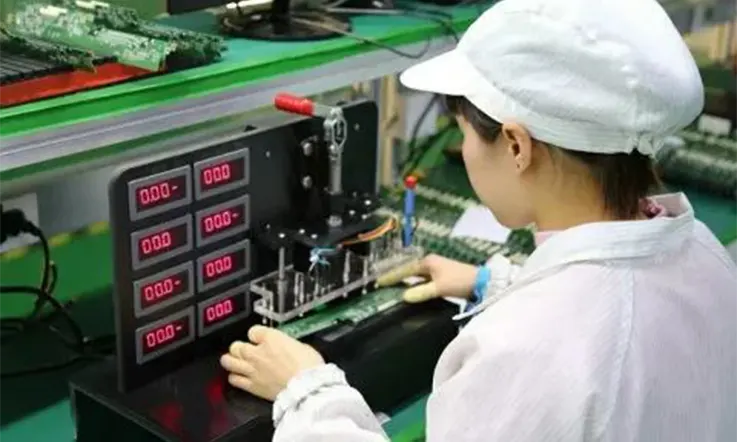
Effective development of electronic hardware requires appropriate test jigs. JarnisTech offers a seamless solution by providing high-quality PCBA test fixture designs for development or production, delivered in as little as one day, to expedite the development process. Test jigs are commonly utilized for installing new firmware and testing product functionality.
Our turnkey PCB assembly service eliminates the bottlenecks and frustrations faced by firmware developers and hardware designers, enabling efficient testing and production. Our test jig solutions eliminate the need for soldering power cables or programming headers to PCBAs, and the nuisance of debugging faulty connections or broken solder joints. By reducing the time needed to construct a production-competent fixture, PCBA functional tests can be developed early, ensuring an efficient and optimized development process.
Our quick turnaround time and high-quality designs reduce production time, streamlining the development process. JarnisTech remains committed to providing reliable and effective test jig designs fitting for PCBAs, enabling efficient development and production.
Definition of PCBA Test Jig ?
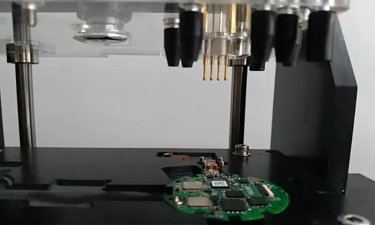
The PCBA test jig functions on a simple and easily understandable principle. The establishment of connections between the pads or test points on the Printed Circuit Board (PCB) is facilitated by metal probes. Once the PCB is powered, the test circuit’s voltage and current values can be obtained using the test jig, allowing for the identification of any normal circuit functions.
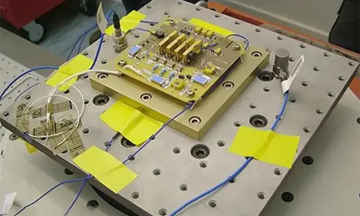
The bespoke nature of the PCBA test jig is determined by the size of the PCB to be tested, the location of test points, and the values to be tested. The manufacturing process primarily utilizes acrylic, plastic, metal probes, a display screen, wire, and a basic PCB circuit board.
As a reliable PCB and assembly manufacturer, we prioritize delivering high-quality test jigs to our clients to ensure the accurate testing of PCBAs. Our test jig designs are tailored to meet specific client requirements, ensuring optimal results during the testing phase. We use only top-of-the-line materials and employ advanced manufacturing processes to ensure the highest quality and reliability of our test jigs.
At our manufacturing facility, we prioritize client satisfaction, ensuring the timely delivery of bespoke test jigs that meet clients’ unique needs for efficient testing of their PCBAs.
How to Design and building a custom PCBA test Jig ?
Designing and building a custom PCBA test jig typically involves the following steps:
● Requirements analysis: Determine the specific testing requirements, including the types of tests to be performed, the test points to be accessed, and the required accuracy and repeatability of the tests.
● Conceptual design: Create a conceptual design for the test jig, taking into account the manufacturing tolerances, accessibility of test points, fixture alignment, and replacement.
● Detailed design: Prepare a detailed design of the test jig, including a detailed fixture layout, contact system, and assembly drawings. This may require the use of 3D CAD modeling software.
● Prototype testing: Build a prototype of the test jig and conduct preliminary testing to ensure it meets the design criteria and testing requirements.
● Test fixture fabrication: Fabricate the final test fixtures, taking into account the precision and accuracy necessary to achieve reliable testing.
● Test platform integration: Integrate the test fixtures with a test platform or test equipment to automate the testing process and ensure high-volume testing.
● Calibration and maintenance: Calibrate the test jig regularly to ensure that testing results remain accurate, and perform regular maintenance to prevent issues and maximize the jig’s lifespan.
Designing and building a custom PCBA test jig can be a complex process, requiring expertise in PCB design, mechanical design, and testing procedures. It is critical to ensure that the final test jig achieves the required accuracy, reliability, and test coverage to ensure the quality of the electronic assemblies.
Types of PCBA test jigs
There are several types of PCBA test jigs, including:
● Bed-of-nails jig: This type of jig uses a grid of spring-loaded pins to make contact with test points on the PCB. The pins can be reconfigured for different PCB designs.
● Flying probe jig: A flying probe jig uses robotic arms with probes to test specific points on a PCB. These types of jigs are useful for low-volume production or when testing complex PCB designs.
● Universal test jig: A universal jig can test multiple PCB designs using interchangeable test fixtures and test platforms. This type of jig offers high flexibility and reduced costs for PCB testing.
● Custom test jig: A custom test jig is designed and built specifically for a particular PCB design. This type of jig can offer higher accuracy and speed for testing, but may have higher costs and longer lead times.
● Functional test jig: A functional test jig tests the full functionality of a PCB by simulating the inputs and outputs of the product. This type of jig is useful for testing complex electronic systems.
The type of PCBA test jig used depends on factors such as the PCB design, test requirements, and budget.
Components of a PCBA Test Jig
The components of a PCBA test jig typically include:
● Test fixtures: These are custom-designed mechanical structures that are used to hold the PCB or individual components in place during testing.
● Interface pins: Interface pins are used to make electrical connections with the PCB or components, providing access to the required test points.
● Contact systems: Contact systems provide the physical connection between the interface pins and the PCB or components.
● Test software: Test software is used to automate the testing process and analyze the results.
● Testing equipment: Testing equipment includes electronic measuring instruments, power supplies, and other equipment necessary to perform the required tests.
● Fixturing and mounting hardware: Fixturing and mounting hardware includes rods, brackets, and screws necessary to hold the fixtures and contact systems in place.
● Cabling and wiring: Cabling and wiring are used to connect the interface pins and contact systems to the testing equipment.
The design of a PCBA test jig can vary depending on the circuit board’s complexity and the types of tests required. The specific components and features of a test jig will depend on the specific testing requirements and the PCB or component design. However, all PCBA test jigs must be designed with precision and accuracy to ensure reliable testing results.
The Purpose of PCBA Test Jig
The PCBA Test Jig plays a crucial role in the entire PCB Assembly and Manufacturing process. It is primarily used for testing the PCBA board after SMT Assembly and Through-Hole Soldering have been completed. The ICT (In Circuit Test) is the most commonly utilized testing method at this stage. This test evaluates the performance of the test points and checks the electrical conductivity of the circuit board, ensuring the correct soldering of the PCB board. The PCBA test jig is an essential piece of equipment for carrying out this testing process.
The quality of the PCBA Test Jig directly affects the effectiveness and pass-through rate of the ICT. Due to its long-term and frequent operation, high requirements are placed on the production quality of this equipment. As a result, it is imperative for PCB manufacturers to prioritize the production quality of the equipment for long-term and frequent usage.
PCBA Testing and the Importance of Test Jigs
PCBA (Printed Circuit Board Assembly) testing is an essential part of the electronic product manufacturing process. The goal of PCBA testing is to ensure that the printed circuit board and its components are properly assembled and functioning correctly.
● PCBA test jigs are tools used to perform the automated testing of electronic assemblies. These jigs help to quickly and accurately test the functionality of the assembled printed circuit boards. By using a test jig, the testing process can be automated, saving time and reducing the potential for costly errors.
● Test jigs can be custom-designed to test specific combinations of components and to verify that they are functioning as intended. They can also detect errors or faults in the PCB assembly process, such as missing components or soldering defects.
● PCBA testing is essential for ensuring the reliability and quality of electronic products. Without proper testing, products may not function as intended, or may fail prematurely, leading to costly repairs and customer dissatisfaction.
● By using PCBA test jigs, electronic manufacturers can increase their production efficiency, improve quality control, and reduce the costs associated with product failures. This makes test jigs a critical tool for ensuring the long-term success and profitability of an electronic manufacturing operation.
PCBA Test Jig: Factors of Considerations and Recommendations
To facilitate the manufacturing of test jigs, the provision of ECAD files is essential as they enable automatic identification of various test characteristics, including test points and mounting holes. Our company acknowledges the importance of this aspect and supports a range of file types for this purpose. Rest assured that we can work with you to ensure we receive the necessary files to create an efficient and effective test jig.
The following file types are supported by our company:
● Gerbers(.zip)
● Eagle (.brd)
● KiCAD (.kicad_pcb)
● Altium Test Point Reports (.csv)
Test Jig Design
When designing a fixture for testing purposes, it is critical to select appropriate components for the test probe card and receptacle from the list of available options. Modifications, removals of guide pins, and additional probes may be necessary depending on the specifics of the design. Additionally, establishing panelization parameters and determining the location of the device under test (DUT) may enable the fixture to conduct tests on an entire panel simultaneously. Prior to finalizing the design, it is essential to carry out a rigorous visual inspection of the fixture to ensure its accuracy and effectiveness. Our team recognizes the importance of these design considerations and strives to deliver custom fixtures that meet the highest standards of quality and reliability.
Test Jig Fabrication
Upon downloading the Design File Package, comprehensive instructions and materials necessary for assembling the fixture are included. The next step entails utilizing the downloaded files to fabricate the plates, which can be achieved by using techniques such as acrylic fabrication, CNC milling, or laser cutting. Our team recognizes the importance of efficiency and precision in fixture assembly and strives to provide our clients with the necessary tools and resources to construct high-quality fixtures.
Test Jig Assembly
Once all probes and guide pins are correctly connected and the test instrumentation is integrated, it is necessary to perform the test. Our team understands that this stage is critical, as the accuracy of the test results hinges on the functionality of the test setup. Therefore, we place significant emphasis on ensuring seamless integration of test instrumentation and conducting thorough quality checks before proceeding to run tests.
Design for Test (DFT)
Building a test fixture for a printed circuit board (PCB) that wasn’t initially designed for testing purposes can prove to be a challenging and costly endeavor. To address this issue, employing a bed-of-nails test jig can significantly simplify the process of testing PCB assemblies. Our team understands that such fixtures can greatly enhance testing capabilities, and thus, we offer the following suggestions to optimize their use:
Single-sided Probing: To simplify and reduce the complexity and cost of testing printed circuit boards (PCBs), it is recommended that all test points be arranged on a single side, ideally on the side containing fewer components. This arrangement is beneficial for both rigid and flexible PCB configurations, as it simplifies the test fixture design, reduces the associated costs, and minimizes the overall complexity of the testing process. Our team recognizes this critical aspect of test fixture design and works closely with clients to ensure that testing solutions are highly efficient and cost-effective.
Test Point Grid Spacing: In the world of printed circuit board assembly (PCBA) testing, Test Point Grid Spacing is a common term used to describe the minimum distance allowable between test locations on the PCB. This spacing can be measured in either mil (a thousandth of an inch) or mm, and there are various grid spacings available for test probes. The most commonly used test point grid spacings include:
● P50 (50mil or 1.27mm spacing).
● P75 (75mil or 1.91mm spacing).
● P100 (100mil or 2.54mm spacing).
In printed circuit board (PCB) design, it is advisable to incorporate the maximum permissible test point spacing. A larger test probe size offers greater durability, and its cost is often lower compared to smaller probes. Based on our experience at JarnisTech, the most common test point spacings we use are 100 mil (2.54 mm) and 75 mil (1.91 mm). These spacings have been proven to offer optimal testing functionality while maintaining the integrity of the PCB.
Test Probe and Test Point Types: To achieve optimal results during testing, it is recommended to use standard pads with a diameter of at least 0.8 millimeters (31.5mil), even though there are various test points and probes available. The majority of probe types are compatible with these pad sizes without encountering any issues. To enhance the reliability of the tester, it is advisable to increase the pad diameter to 1 millimeter. Additionally, an overview of various test points and their corresponding compatible test probes is provided below.
1. Terminals and Posts: A square terminal or post, which is soldered to the board, is utilized to create a component’s terminal or post. For testing purposes, slotted (self-cleaning) cups are highly recommended for contacting these test points when facing upwards. Additionally, serrated or flat tips may also be employed. It is noteworthy that the cup tips will automatically align with the terminals or post, providing added convenience during testing.
2. Leads: When the lead of a through-hole component is soldered to the PCB board, a lead test point is created, establishing a connection between the component and the board. Cupped probe tips are one way of testing this connection, although serrated probe tips are typically more durable when compared to cupped probe tips.
3. Pogo Contact Pads: On a printed circuit board (PCB), simple pads that lack solder coverage are referred to as pad test points (without solder paste). Employing a pad that is at least 0.8 millimeters in diameter, with a preference for maximum diameter, can enhance the contact reliability of the probes with the pads. Crown tips are suitable for establishing contact with clean, flat solder pads, although they require periodic maintenance. Needle and Spear tips are advantageous for carrying out precise tests on flux-coated solder pads.
To ensure that the PCB designs you develop are testable, the following checklist can serve as a helpful guide:
● Maintain a spacing of greater than 1.91 millimeters between test sites.
● Have at least one test point available for every net that requires testing.
● Employ pads with a diameter of 1 millimeter or more and free of solder paste for each test point.
● Position all test points on the top or bottom of the PCB board, considering the least congested side of the board wherever possible.
Which Common Faults of PCB Assembly That Need PCBA Testing ?
● Plating Voids: Contamination in the material used for plated copper inside the through-hole walls of a printed circuit board (PCB) can result in inadequate plating. Poor plating can lead to suboptimal current transfer across PCB layers. To avoid this issue, it is necessary to thoroughly clean the holes after drilling to remove any contaminants.
● Solder Bridges: Solder bridging or shorts can occur when the solder forms an unintended conductive path between the leads or pins of an electronic component during the printed circuit board (PCB) assembly process. These bridges can be minuscule and difficult to detect in a PCB assembly without sufficient testing tools. An undetected short in a PCB leaving the manufacturing line can result in damaged PCB traces or even exploded components. Inadequate solder mask between pads and pins is the most common cause of solder bridges, while inconsistent alignment of components and the PCB can also lead to the issue.
● Open Solder Joints: An issue that can arise during the printed circuit board (PCB) assembly process involves the incomplete soldering between the component lead and the pad. This problem can be attributed to several factors, such as inadequate wetting, insufficient spacing between the component lead and PCB pad, low-quality solder paste, and misalignment of components.
● Insufficient Wetting: In an ideal scenario, molten solder would uniformly coat the leads on a printed circuit board (PCB). However, inadequate wetting can occur in certain cases such as the formation of extra solder mounds or partial coverage of leads (known as de-wetting). Additionally, insufficient wetting may arise due to non-wetting caused by de-wetting. Concerns such as these can be prevented by utilizing top-notch solder and PCB assembly equipment.
● Component Shift or Misalignment: During the reflow stage of the printed circuit board (PCB) assembly process, inadequate epoxy material can lead to component misalignment and floating. When temperatures are unstable, pads may also form, which can result in component mismatches. Furthermore, pads themselves can cause shifts in components during assembly.
Challenges and Best Practices When Using PCBA Test Jigs
Some challenges that can be encountered when using PCBA test jigs and best practices to address them include:
Challenges:
● Test coverage: It can be challenging to ensure that the PCBA test jig covers all the required test points on the PCB.
● Tooling and fixturing: Fixtures and tooling must be accurately designed and built to ensure proper alignment and reliable connections with the test points.
● Accuracy and repeatability: The test jig should offer consistent results, with minimal variation between test cycles.
● Maintenance and calibration: The PCBA test jig should be regularly maintained and calibrated to ensure it continues to provide accurate results.
Best practices:
● Early involvement in the design process: Test engineers should be involved in the design process as early as possible to ensure that the test points are easily accessible and can be tested reliably.
● Standardization: Standardized tooling and fixturing can reduce variation and improve accuracy, repeatability, and test coverage.
● Automation and software controls: Automation and software controls can reduce the potential for human error and ensure consistent results.
● Proactive maintenance and calibration: Regular maintenance and calibration can help prevent issues before they affect test results, reducing downtime and costs.
● Documentation and traceability: A comprehensive documentation and traceability system can help identify issues and verify the quality of the testing process.
Cost Considerations and ROI for PCBA Test Jigs
Cost considerations and ROI (Return on Investment) for PCBA test jigs may include:
● Upfront costs: The costs for designing, building, and validating a PCBA test jig can vary depending on the complexity of the jig and the required specifications.
● Operating costs: The ongoing costs for operating and maintaining a PCBA test jig include repair or replacement of any damaged parts or components and regular calibration.
● Downtime: Downtime can occur when the test jig is being built, maintained, or repaired, and can impact production schedules and profitability.
● Quality improvements: Improvements in product quality achieved through PCBA testing can lead to reduced product defects and lower product returns.
● Reduction in field failures: A decrease in field failures can result in reduced warranty and repair costs and an increase in customer satisfaction.
● Increased production efficiency: PCBA test jigs can help improve production efficiency by automating the testing process, reducing manual labor, and increasing throughput.
Ultimately, the cost considerations and ROI for PCBA test jigs will vary based on the specific circumstances of each application. Careful consideration of these factors can help justify an investment in PCBA test jigs and ensure that the investment provides a positive return.
Future Outlook for PCBA Testing and Test Jigs
The future outlook for PCBA functional electronic testing and test jigs is promising as the demand for electronic products continues to grow, and manufacturers focus on improving product quality and reducing costs.
Some potential trends and developments that may impact PCBA testing and test jig technology in the future include:
● Increased use of Artificial Intelligence (AI) and Machine Learning (ML) in testing equipment and software, enabling more sophisticated and automated testing capabilities.
● Advancements in Wireless and Bluetooth technologies may create a shift in the types of products manufactured, necessitating the development of newer testing methods.
● Higher Integration with the Internet of Things (IoT) can open up new opportunities for testing, monitoring, and diagnosing faults remotely.
● Miniaturization of electronics components will require more precise and sophisticated test jigs capable of handling smaller components and more complex circuitry.
● Developments in IoT, AI, and ML enable data sharing, cloud computing, and machine interconnectivity, enabling faster data processing and analysis to deliver accurate results.
Despite the potential challenges, the growing demand for electronic products, coupled with the need to improve testing efficiencies and capabilities, is likely to drive future innovations in PCBA testing and test jig technology.
Summary
Jarnistech is a China-based turnkey PCB manufacturer committed to providing comprehensive PCB assembly services. As part of our quality assurance process, we perform a thorough functional test on every PCB assembly. We collaborate closely with our clients to develop effective test protocols that meet their requirements. Our aim is to work as your partner and ensure that the construction of your PCB assembly is of high quality, completed on time, and cost-effective. Please don’t hesitate to contact us if you require the services of a contract manufacturer that prioritizes collaborative efforts with their clients.


