As semiconductor devices integrate greater power within smaller footprints, thermal management becomes a direct engineering obstacle. Excess heat compromises the operational performance, reliability, and service life of electronic systems. When the heat dissipation capacity of conventional materials like FR-4 is met, a higher-performance substrate becomes necessary. Aluminum Nitride (AlN) ceramic substrates are engineered specifically to address these demanding thermal conditions.
The Fundamental Science of Aluminum Nitride (AlN)
The performance of an Aluminum Nitride (AlN) PCB is a direct outcome of its fundamental material science. The material’s distinct properties originate from its atomic structure and the physical principles that define its behavior.
The Wurtzite Crystal Structure and Its Effect on Performance
The atomic arrangement of AlN is a hexagonal wurtzite structure. In this configuration, each aluminum atom is tetrahedrally coordinated with four nitrogen atoms, and vice-versa. These atoms are held by strong covalent bonds, creating a stiff and highly ordered lattice. This stable structure results in several of AlN’s beneficial traits, including its high mechanical hardness and, most notably, its capacity for efficient thermal energy transfer.
The Physics of Phonon-Based Thermal Conduction in AlN
Unlike metals where heat is conducted by free electrons, in dielectric materials like AlN, heat transfer occurs through lattice vibrations. These quantized waves of atomic vibration are known as phonons. The crystal lattice can be imagined as a tightly ordered three-dimensional grid of atoms connected by springs. When heat is introduced, it causes the atoms to vibrate, and these vibrations propagate through the structure as waves.
The efficiency of this phonon transport determines the material’s thermal conductivity. The highly ordered, low-defect nature of the AlN wurtzite lattice, combined with the low mass of its constituent aluminum and nitrogen atoms, allows these phonon waves to travel with minimal scattering. This unimpeded flow of vibrational energy is what gives AlN its exceptionally high thermal conductivity.
Raw Materials and Synthesis Methods
High-purity AlN powder, the precursor for an AlN substrate, does not occur naturally and must be produced through meticulous industrial processes. Two prevalent synthesis methods are:
●Direct Nitridation: This method involves exposing high-purity aluminum powder to a pure nitrogen or ammonia atmosphere at elevated temperatures (typically 800°C to 1200°C). The aluminum reacts with the nitrogen to form AlN powder. The main difficulty is managing the highly exothermic reaction to achieve uniform particle size and prevent oxide impurities.
●Carbothermal Reduction and Nitridation (CRN): In this process, alumina (Al₂O₃) is mixed with a carbon source and heated to very high temperatures (1500°C to 1800°C) in a nitrogen atmosphere. The carbon reduces the alumina, and the resulting aluminum reacts with the nitrogen. This method can yield very high-purity AlN powder, as the starting alumina is available at exceptional purity levels.
| Synthesis Method | Process Temperature | Starting Materials |
| Direct Nitridation | 800–1200°C | High-purity Al powder + N₂/NH₃ |
| Carbothermal Reduction & Nitridation | 1500–1800°C | Al₂O₃ + Carbon + N₂ |
| Typical AlN Powder Purity | >99.9% | – |
| Particle Size (Post-processing) | Submicron to few μm | – |
The mastery of these synthesis routes, followed by precise sintering processes, determines the final quality and dependability of an AlN substrate. It is this advanced process control that ensures the material delivers its specified thermal and mechanical performance in demanding applications.
A Review of the Core Properties of AlN Substrates
The performance of an AlN ceramic PCB is defined by the intrinsic properties of its substrate material. A detailed review of these characteristics illuminates how AlN meets the requirements of demanding applications by examining its thermal, electrical, mechanical, and chemical attributes.
Advanced Thermal Properties
The thermal behavior of AlN dictates the stability of an electronic assembly. Achieving these outcomes depends on both the quality of the sintered ceramic and the precision of subsequent assembly processes.
| Thermal Property | Typical Value | Description |
| Thermal Conductivity | 170–220 W/m·K | Enables efficient heat dissipation from high-power components |
| Coefficient of Thermal Expansion | 4.0–6.0 ppm/°C | Matches well with silicon, reducing thermo-mechanical stress |
| High-Temperature Stability | >1000°C (in controlled atmospheres) | Maintains integrity during high-temp processes like die bonding and brazing |
●High Thermal Conductivity: AlN exhibits thermal conductivity typically in the range of 170-220 W/mK. This property, arising from efficient heat transfer through lattice vibrations (phonons), allows heat to spread rapidly from a concentrated source like a semiconductor die. This action lowers the peak junction temperature and contributes to improved device efficiency and a longer operational lifetime.
●Low Coefficient of Thermal Expansion (CTE): With a CTE of approximately 4.0-6.0 ppm/°C, AlN’s expansion behavior is very similar to that of silicon (Si). This compatibility reduces the thermo-mechanical stress at the die-substrate interface during thermal cycling, mitigating a common source of failure in power modules and large-area chip-on-board assemblies.
●High-Temperature Stability: The material maintains its structural and electrical integrity well above 1000°C in controlled atmospheres. This allows it to function in extreme operating environments and withstand high-temperature manufacturing processes, such as eutectic die bonding and brazing, without degradation.
Electrical Insulation and Dielectric Performance
An effective substrate must manage heat while providing robust electrical isolation. These characteristics are a function of the material’s purity and structural integrity, which are controlled during manufacturing.
| Electrical Property | Typical Value | Significance |
| Dielectric Strength | >15 kV/mm | Withstands high voltages, ensuring insulation between circuits |
| Dielectric Constant (εr) | ~8.9 | Supports predictable signal behavior in RF/microwave frequencies |
| Dielectric Loss Tangent (tanδ) | ~10⁻³ | Minimizes power losses at high frequencies |
| Volume Resistivity | >10¹⁴ Ω·cm | Prevents leakage current, enhancing circuit isolation in dense designs |
●High Dielectric Strength: With a dielectric strength exceeding 15 kV/mm, AlN withstands very high voltage gradients without suffering from electrical breakdown. This makes it a reliable material choice for high-voltage power electronics where operational safety is a priority.
●Low Dielectric Constant and Loss Tangent: AlN features a moderate dielectric constant (εr) of around 8.9 and a very low dielectric loss tangent (tanδ) of approximately 10⁻³. This translates to minimal signal power loss for RF and microwave circuits and enables the design of high-frequency components with predictable performance.
●High Volume Resistivity: The volume resistivity of AlN is exceptionally high (>10¹⁴ Ω·cm), indicating its strong ability to prevent current leakage between conductive traces. This helps ensure circuit isolation and stability in densely packed designs.
Mechanical Strength and Reliability
A substrate serves as the physical foundation for delicate components. AlN’s ceramic nature provides a level of mechanical stability beyond that of polymer-based PCBs, though this robustness must be preserved through controlled handling and assembly techniques.
| Mechanical Property | Typical Value | Implication |
| Hardness (Knoop) | ~1100 kg/mm² | High surface wear resistance |
| Young’s Modulus | ~330 GPa | Provides stiffness and dimensional stability under load |
| Fracture Toughness | 2.5–3.5 MPa·m¹/² | Moderate resistance to crack propagation under mechanical stress |
●Hardness and Rigidity: AlN is a very hard material (approx. 1100 kg/mm² on the Knoop scale) with high wear resistance. Its high Young’s modulus provides rigidity, ensuring the substrate remains flat under thermal load or during assembly and offering a stable platform for components.
●Fracture Toughness: AlN exhibits a fracture toughness of 2.5-3.5 MPa·m¹/², indicating its resistance to crack propagation from a pre-existing flaw. While careful handling is still needed, this level of toughness is sufficient for many applications, including those subject to mechanical vibration.
Chemical Compatibility and Resistance
The chemical inertness of a substrate affects its performance in harsh environments and its suitability for certain manufacturing steps. This behavior informs the selection of compatible materials and chemistries used during fabrication and assembly.
●Resistance to Molten Metals: AlN is non-reactive with molten aluminum and many other molten metals and salts. This stability is advantageous during high-temperature soldering and brazing processes.
●Behavior with Acids and Alkalis: AlN shows good resistance to most acids but can be eroded by alkaline solutions, particularly at higher temperatures. Upon exposure to moisture, a thin, self-passivating layer of aluminum oxide forms on the surface, protecting the underlying material from further oxidation.
Comparative Analysis: AlN Alongside Specialized PCB Technologies
Selecting the optimal substrate requires an understanding of the trade-offs between different high-performance materials. While AlN offers a potent combination of properties, other specialized technologies have merits in specific contexts. This comparison positions AlN against other well-known alternatives for high-performance electronics.
AlN vs. Insulated Metal Substrate (IMS / MCPCB)
This comparison is common for thermal-focused applications.
| Property | AlN Substrate | IMS / MCPCB |
| Structure | Monolithic ceramic | Metal base + polymer dielectric + Cu |
| Thermal Conductivity | 170–220 W/m·K | ~1–3 W/m·K (dielectric layer) |
| CTE Matching with Silicon | Good (~4–6 ppm/°C) | Poor–Moderate (Al base ~23 ppm/°C) |
●Structure: An IMS board, or Metal Core PCB, consists of a metal baseplate (usually aluminum), a thin dielectric prepreg layer, and a copper circuit layer. In contrast, an AlN substrate is a solid, monolithic ceramic.
●Thermal Path: The main thermal bottleneck in an IMS board is the polymer dielectric layer. Its thermal conductivity is low (~1-3 W/mK), which restricts the overall thermal performance. In AlN, the entire bulk of the substrate is highly thermally conductive (170+ W/mK).
●Performance Trade-off: For heat sinking in DC or low-frequency applications where cost is a primary consideration, IMS is a viable solution. AlN is selected when an application demands superior thermal performance combined with high voltage isolation, excellent high-frequency characteristics, or direct chip-on-board mounting where CTE matching is a factor. Realizing these benefits relies on a fabrication process that supports both the ceramic and the advanced assembly techniques it enables.
AlN vs. High-Frequency Laminates (e.g., Rogers Materials)
This comparison is frequent in RF and microwave applications.
| Property | AlN Substrate | Rogers Materials (e.g., RO4000) |
| Dielectric Constant (Dk) | ~8.9 | ~3.38–3.55 (stable with frequency) |
| Dissipation Factor (Df) | ~0.001 | ~0.002–0.004 |
| Thermal Conductivity | 170–220 W/m·K | <1 W/m·K |
●Core Strength: Materials like the RO4000 series are hydrocarbon ceramic laminates developed for electrical performance at high frequencies. They offer very low and stable dielectric constants (Dk) and dissipation factors (Df), making them a cost-effective choice for many RF circuit designs.
●Thermal Management: While better than FR-4, the thermal conductivity of these laminates is modest (typically < 1 W/mK). They can manage heat from low or medium-power RF components but face challenges with high-power GaN or LDMOS transistors.
●Performance Trade-off: For low-power RF designs, Rogers materials offer a good balance of performance and cost. AlN becomes the choice when the RF application also generates substantial heat. Successfully integrating high-power devices on AlN requires manufacturing expertise that merges RF circuit principles with effective thermal management at the assembly level.
AlN vs. High-Temperature Polymers (e.g., Polyimide)
Polyimide is noted for its high temperature resistance relative to other polymers.
| Property | AlN Substrate | Polyimide PCB |
| Max Operating Temperature | >1000°C | ~250–300°C (glass transition) |
| Thermal Conductivity | 170–220 W/m·K | ~0.2–0.4 W/m·K |
| Flexibility | Rigid | Flexible |
●Temperature Ceiling: Polyimide has a high glass transition temperature (Tg > 250°C), making it suitable for high-temperature environments where FR-4 would degrade. However, AlN operates in a different thermal class, remaining stable at temperatures exceeding 1000°C.
●Thermal Conductivity: As a polymer, polyimide has very low thermal conductivity (~0.2-0.4 W/mK). It can survive high temperatures, but it cannot effectively dissipate heat from a component. AlN accomplishes both.
●Performance Trade-off: Polyimide is the solution for applications that require mechanical flexibility in high-temperature environments. AlN is for rigid applications that require not just survival at high temperatures, but also active, high-efficiency thermal dissipation. Its use is characteristic of designs where the assembly process is tailored to a rigid ceramic platform.
AlN (HTCC) vs. Low-Temperature Co-fired Ceramic (LTCC)
This is a comparison between two different ceramic circuit technologies.
| Property | AlN (HTCC) | LTCC |
| Firing Temperature | ~1800°C | <900°C |
| Conductor Materials | Refractory metals (e.g., W, Mo) | Noble metals (Ag, Au) |
| Thermal Conductivity | 170–220 W/m·K | ~2–5 W/m·K |
●The Firing Process: As a High-Temperature Co-fired Ceramic (HTCC), AlN is fired at ~1800°C, requiring refractory metals like tungsten for internal conductors. LTCC uses a glass-ceramic composition that fires at a much lower temperature (<900°C).
●Conductors & Performance: LTCC’s lower firing temperature allows the use of highly conductive co-fired metals like silver and gold for internal traces. This can result in lower signal loss for certain high-frequency circuits.
●Performance Trade-off: LTCC is an excellent choice for complex, high-density RF modules where conductor loss is the main concern. AlN is selected when the requirements are superior mechanical strength, hermeticity, and high thermal conductivity. This choice is typical for applications where the final package must offer maximum durability and heat removal, demanding specialized co-firing and hermetic sealing capabilities.
The Manufacturing Process: From AlN Powder to Precision Substrate
The transformation of raw AlN powder into a flat, dense, and reliable ceramic substrate is a multi-stage process requiring precision and control. Each step is managed meticulously, as any deviation can affect the final thermal, mechanical, and electrical properties of the material.
Powder Preparation and Purity Control
The process begins with the AlN powder itself, where particle size distribution, morphology, and purity define the starting point. The powder is often milled to break up agglomerates and achieve a uniform particle size. Sintering aids—proprietary chemical additives—are introduced in minute, precisely metered quantities. These aids facilitate densification at lower temperatures by forming a liquid phase during firing that helps rearrange and bond the AlN grains.
Substrate Forming via Tape Casting
For producing thin, flat ceramic sheets, tape casting is the predominant industrial method. The process includes these steps:
●Slurry Formulation: The AlN powder and sintering aids are mixed with a solution of solvents, binders (polymers for green-tape strength), and plasticizers (for flexibility). This mixture is milled for many hours to create a homogenous, viscous liquid known as a slurry.
●Casting: The slurry is fed onto a moving carrier film. It passes under a “doctor blade,” a precisely machined knife edge held at a specific height, which spreads the slurry into a thin, uniform layer of controlled thickness.
●Drying: The cast tape travels through a long, temperature-controlled drying oven. Solvents evaporate slowly, leaving a flexible, leather-like sheet of ceramic powder held together by the binder. This “green tape” must be flat and uniform, qualities that depend heavily on the precision of the casting and drying stages.
The Sintering Stage: Atmosphere and Temperature Control
Sintering is the heat treatment that transforms the fragile green tape into a hard, dense ceramic. This is the most sensitive stage of production.
●Binder Burnout: The green tape is first heated slowly in a controlled atmosphere to completely remove the organic binders and plasticizers without introducing defects.
●High-Temperature Sintering: The temperature is then raised to between 1800°C and 1900°C in a nitrogen-rich, oxygen-free atmosphere, which is necessary to prevent the AlN from decomposing. During this stage, the sintering aids melt, and capillary action pulls the AlN grains together. The particles then fuse through solid-state diffusion, eliminating porosity and causing the part to shrink significantly (typically 15-20%) into a solid ceramic. Precise control of the temperature profile and atmosphere determines the final density and thermal conductivity.
Post-Sintering Processing and Surface Finishing
The sintered AlN substrate, while dense, does not yet have the dimensions or surface finish required for microelectronics.
●Lapping: Substrates are lapped using diamond abrasives to achieve a specific thickness and a high degree of flatness. This grinding process removes material from both sides of the substrate simultaneously.
●Polishing: For applications requiring an exceptionally smooth surface, such as for thin-film circuits, the lapped substrates undergo a final polishing step. This uses progressively finer diamond slurries to achieve a mirror-like finish with a surface roughness (Ra) of less than 0.1 µm.
Metallization Technologies for AlN: Creating the Conductive Pathways
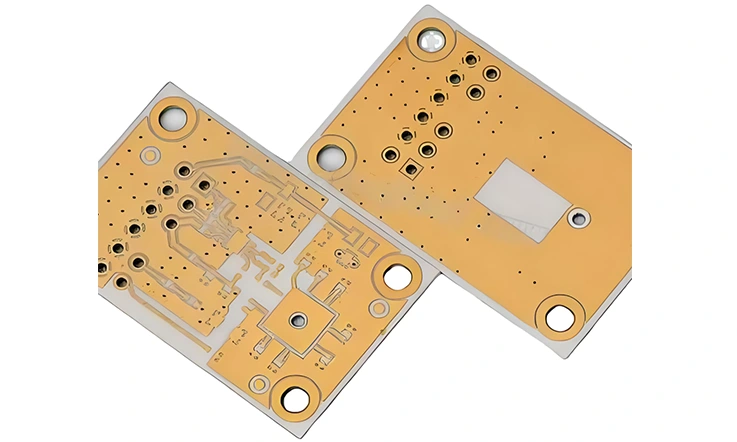
An un-metallized ceramic is just an insulator. To turn it into a PCB, conductive pathways must be formed on its surface. The method of metallization defines the board’s current handling capacity, trace resolution, and reliability. The adhesion of this metal layer to the inert ceramic surface is a primary engineering challenge.
An Introduction to Metallization Adhesion Mechanisms
Bonding metal to a ceramic is fundamentally different from bonding it to a polymer like FR-4. It relies on complex physical and chemical interactions at the interface. Different technologies leverage different mechanisms—from mechanical interlocking and van der Waals forces in thin-film processes to the formation of new chemical compounds in bonding and brazing technologies. The choice of method is a balance of performance requirements, feature size, and cost.
Thin-Film Technology: Direct Plated Copper (DPC)
DPC is an additive process for creating very fine-featured circuits.
●Surface Preparation: The polished AlN substrate is meticulously cleaned.
●Seed Layer Deposition: A thin adhesion layer (e.g., Titanium) followed by a thin copper seed layer is deposited onto the entire substrate surface using a vacuum technique like sputtering. The adhesion layer forms a strong chemical bond with the ceramic.
●Photolithography: A photoresist is applied, exposed to UV light through a circuit-pattern mask, and developed, leaving the circuit pattern exposed.
●Electroplating: The substrate is submerged in an electroplating bath, and copper is selectively plated onto the exposed seed layer to the desired final thickness.
●Strip and Etch: The photoresist is stripped away, and the thin seed layer in the non-circuit areas is chemically etched off, leaving the final, isolated copper circuitry. DPC offers exceptional trace definition, making it suitable for high-frequency applications and densely packed designs.
Thick-Film Technology: Screen Printing and Firing
This method involves screen-printing a specially formulated conductive paste (containing metal particles, glass frit, and an organic vehicle) onto the AlN substrate. The printed substrate is then fired at high temperatures (around 850°C). During firing, the organic vehicle burns off, and the glass frit melts, bonding the metal particles to each other and to the ceramic surface. Thick-film offers a cost-effective solution for simpler circuits and conductor pads, though with lower resolution than DPC.
Direct Bonded Copper (DBC)
DBC is the workhorse technology for high-power modules. The process involves placing a pre-oxidized copper foil onto the AlN substrate and heating the assembly to around 1065°C in a controlled atmosphere. At this temperature, a eutectic reaction occurs between the copper and its oxide, creating a liquid phase that chemically bonds the foil directly to the ceramic. The result is a substrate with thick copper layers (typically 127 to 635 µm thick) that can handle hundreds of amps and provide outstanding heat spreading.
Active Metal Brazing (AMB)
For applications demanding the highest level of reliability and thermal cycling performance, AMB is employed. This process uses a brazing alloy containing an “active” element, such as titanium. When heated in a vacuum furnace, the active element reacts with the Aluminum Nitride, forming a new layer that the molten braze can wet and bond to. This creates an exceptionally strong and hermetic bond between the copper foil and the AlN substrate, often exceeding the strength of a DBC bond.
Designing for Manufacturability (DFM) with AlN Ceramic PCBs
Designing a circuit for an AlN substrate differs from designing for FR-4. Acknowledging the material’s unique properties and manufacturing processes during the design phase can prevent costly revisions and improve the final product’s reliability.
Layout Guidelines for Thermal Management
The primary reason to select AlN is for heat removal, and the layout must be optimized for this function.
●Copper Planes: Use large, solid copper planes directly under heat-generating components to maximize the area for lateral heat spreading.
●Wide Traces: High-current paths should be made as wide as feasible not only for electrical capacity but also to serve as effective thermal conduits.
●Thermal Vias: An array of vias under a component pad creates a low-resistance thermal path through the substrate to a backside heatsink. The density and diameter of these vias should be maximized within mechanical limits to lower the overall thermal resistance.
Mechanical Design: Brittleness and Tolerances
While strong, AlN is a brittle ceramic, making mechanical details a central focus of the design.
●Corner Radii: Avoid sharp internal corners in any machined cutouts. Adding a small radius to inside corners distributes stress and reduces the risk of crack initiation.
●Edge Proximity: Keep traces and components away from the substrate’s physical edges and any screw holes or cutouts, as these are areas of high stress concentration.
●Scribing and Breaking: For arrayed PCBs, designs must incorporate scribe lines. The depth and location of these lines are planned to allow for a clean, controlled break when separating individual boards after assembly.
Considerations for CTE Mismatch with Large Components
While AlN’s CTE has a close correspondence with silicon, it may not align with all materials in an assembly (e.g., copper heatsinks). For large components, the cumulative stress from a small CTE mismatch can be substantial. Finite Element Analysis (FEA) is often used during the design phase to model these stresses and inform the selection of appropriate solder or epoxy interfaces that can absorb the strain.
Design Collaboration for Successful Assembly
The final details of the layout, such as pad design, have a direct bearing on the quality and yield of the assembly process.
●Solder Mask Definition: Where solder masks are applied, their registration and definition are precisely controlled to prevent solder wicking and ensure proper fillet formation.
●Surface Finish: The choice of surface finish on the copper pads (e.g., ENIG, ENEPIG, bare copper) is selected based on the assembly method (e.g., wire bonding, soldering) and the requirements for long-term reliability.
To discuss the specific requirements of your design with a technical specialist, you are invited to initiate a consultation.
Advanced AlN Fabrication Capabilities
Beyond flat substrates with surface circuitry, advanced fabrication techniques create complex three-dimensional structures and highly precise features, expanding the application space for AlN.
Laser Machining: Precision Cutting, Drilling, and Scribing
Lasers are the primary tool for shaping and machining hard, brittle AlN. High-powered UV or CO₂ lasers can be used for:
●Substrate Cutting: Profiling the substrate to complex, non-rectangular shapes.
●Via Drilling: Creating through-holes with high precision and aspect ratios. Laser drilling is often faster and more flexible than mechanical drilling for small-diameter vias.
●Scribing: Creating shallow, precise lines for controlled “snap-singulation” of arrayed boards.
●Material Ablation: Selectively removing metallization or ceramic material to create specific circuit features or recessed pockets.
Multilayer Co-fired AlN (HTCC-AlN) for 3D Integration
To achieve maximum circuit density and integration, a multilayer approach is used. This process involves co-firing stacked layers of ceramic “green tape” to form a monolithic block with intricate internal wiring, buried passive components, and vertical interconnects. This HTCC (High-Temperature Co-fired Ceramic) technology allows for the creation of highly compact and hermetically sealed modules, where the ceramic substrate itself becomes the component package.
Cavity Formation for Component Embedding
By laminating green tape layers with pre-punched cutouts, cavities can be formed within the AlN substrate during the co-firing process. These recessed pockets allow for semiconductor dice or other components to be embedded directly into the substrate. This lowers the overall profile of the assembly, shortens bond wire lengths to improve high-frequency performance, and can enhance thermal transfer by bringing the heat source closer to the bulk of the ceramic.
Quality Assurance and Reliability Testing for AlN PCBs
The fabrication of a high-performance AlN PCB is coupled with a rigorous quality assurance regimen. This testing verifies that every substrate meets its specified performance and will function reliably throughout its operational life.
Non-Destructive Testing: Scanning Acoustic Microscopy (SAM)
SAM is a non-destructive technique used to inspect the internal integrity of a substrate, particularly DBC and AMB structures. It uses high-frequency ultrasound to create an image of the bond interface between the copper and the ceramic. This can reveal defects such as voids (un-bonded areas), delaminations, or cracks that are invisible from the surface. A low-void bond interface is a direct indicator of a high-quality thermal path.
Thermal Performance Verification
To ensure reliability under operational conditions, substrates undergo thermal testing.
●Thermal Cycling: Samples are repeatedly cycled between temperature extremes (e.g., -40°C to +150°C) for hundreds or thousands of cycles. This simulates a lifetime of power-on/power-off sequences and tests the resilience of the metallization bond against fatigue from CTE mismatch.
●Thermal Shock: This is a more aggressive test where substrates are rapidly transferred between hot and cold liquid baths. It challenges the material’s ability to withstand sudden, extreme temperature changes without cracking or delamination.
Electrical Integrity Testing
Electrical performance is verified through multiple methods. High-voltage isolation (Hipot) testing applies a high voltage between isolated conductors to ensure there is no dielectric breakdown. For high-frequency circuits, Time-Domain Reflectometry (TDR) can be used to measure the characteristic impedance of transmission lines, verifying that the fabricated circuit matches its design specification.
Integrated PCBA on AlN: A Specialized Assembly Process
Mounting components onto an AlN PCB is a specialized discipline that requires different materials and process controls than standard FR-4 assembly. An integrated approach, where substrate fabrication and assembly are closely linked, yields superior results.
Solder Paste and Reflow Profile Selection for AlN
The high thermal conductivity of AlN presents a challenge for soldering: the substrate wicks heat away from the solder joint so effectively that achieving a proper reflow can be difficult.
●Solder Selection: Solder alloys are chosen based on the application’s operating temperature. For high-power devices, high-melting-point solders (like high-lead or AuSn eutectic alloys) are used to ensure the joint remains solid during operation.
●Reflow Profile: The reflow oven temperature profile must be optimized. It often requires a longer soak time and higher peak temperature to deliver sufficient thermal energy to the solder joints and overcome the heat-sinking effect of the AlN.
Die-Attach Materials and Processes
Attaching a bare semiconductor die to the AlN substrate is a decisive step in the assembly process. The die-attach material serves as both a mechanical bond and a thermal interface.
●Eutectic Bonding: A process like Au-Si eutectic bonding creates a direct, void-free metallic bond between the die and a gold-plated pad, offering excellent thermal performance.
●Sintered Silver: Nanosilver pastes can be used as a die-attach material. Under pressure and heat, the silver particles sinter together to form a solid, highly conductive silver layer, providing a robust, fatigue-resistant bond for high-power applications.
●Conductive Epoxies: While offering lower thermal performance, thermally conductive epoxies provide a more compliant bond that can help absorb some thermo-mechanical stress.
Heavy Gauge Wire and Ribbon Bonding
High-power modules require electrical connections that can handle high currents. This is achieved using heavy gauge aluminum or copper wires (up to 500 µm in diameter) or flat ribbons. Ultrasonic wedge bonding is the typical process. Bonding to the hard, smooth metallized surface of an AlN PCB requires optimized bonding parameters (ultrasonic power, force, and time) to create a reliable, low-resistance connection without damaging the underlying substrate.
Application Note: Thermal and Layout Strategies for High-Density UV-C LED Arrays on AlN Substrates
High-power, deep-ultraviolet (UV-C) LED arrays, used in water and air purification systems, present a multi-faceted design challenge. The wall-plug efficiency of these LEDs is highly sensitive to junction temperature, and the intense UV radiation they emit can rapidly degrade many organic materials, including conventional PCB substrates. This section outlines strategies for leveraging AlN substrates to address these challenges, ensuring both high performance and long-term reliability.
Thermal Path Optimization
The objective is to create the lowest possible thermal resistance path from the LED die to the ambient environment.
●Thermal Via Arrays: For each LED footprint, a dense array of thermal vias should be designed directly under the thermal pad. These vias act as parallel conduits, channeling heat through the AlN to a backside heatsink. The number and diameter of vias should be maximized.
●DBC for Bulk Heat Spreading: Given the concentrated heat flux from a dense LED array, Direct Bonded Copper (DBC) is often the preferred metallization. The thick copper layer (≥200 µm) provides exceptional lateral heat spreading, evening out hotspots between individual LEDs before the heat enters the AlN bulk.
●Interface Material Selection: The choice of Thermal Interface Material (TIM) between the AlN substrate and the final system heatsink represents a final, influential link in the thermal chain and must not become a bottleneck.
Electrical Layout and Material Stability
●Current-Balancing Traces: In series/parallel array designs, trace widths and lengths must be managed to ensure uniform current distribution. Uneven current leads to brightness variations and can cause some LEDs to fail prematurely.
●UV-Resistant Surface Finish: The substrate’s exposed surfaces must be stable under prolonged, high-intensity UV-C exposure. AlN itself is exceptionally stable. The copper traces should be protected by a noble metal surface finish, such as Electroless Nickel Electroless Palladium Immersion Gold (ENEPIG), which prevents oxidation and provides a robust, solderable surface without using organic solder masks that would otherwise degrade.
Case Study: Enhancing the Reliability of a 5G GaN RF Power Amplifier
While the preceding sections have detailed the technical attributes of AlN, this case study demonstrates their application in solving a complex, real-world engineering problem. It examines the thermal and reliability challenges faced in a high-power Gallium Nitride (GaN) RF amplifier designed for 5G infrastructure. The following sections will outline the initial challenge, detail the integrated solution that combined a hybrid AlN substrate with comprehensive engineering support, and present the quantifiable improvements in thermal performance and projected reliability. This serves as a practical example of how a systems-level approach, from material selection through final assembly, directly addresses performance bottlenecks.
The Challenge
A client developing a high-power Gallium Nitride (GaN) based RF power amplifier for a 5G macro base station faced a persistent reliability issue. The amplifier, built on a high-frequency laminate substrate, experienced thermal throttling during peak operation. The high junction temperatures of the GaN-on-SiC power transistors were reducing the device’s Mean Time Between Failures (MTBF) to unacceptable levels, affecting the system’s field reliability.
The Solution
A comprehensive redesign of the amplifier’s substrate was executed. The new design featured a hybrid AlN substrate where a DBC section with a thick copper base was used for the main power stage, providing maximum heat dissipation for the mounted GaN transistors. The surrounding low-power RF signal paths and matching networks were created using fine-featured DPC on the same monolithic AlN substrate. This approach optimized both thermal performance and high-frequency signal integrity. An end-to-end service—including thermal simulation, DFM review, AlN fabrication, and precision component assembly—was utilized.
The Results
Post-implementation analysis demonstrated a substantial improvement in performance and reliability:
1.Quantitative Thermal Improvement: In-situ thermal imaging and thermocouple measurements showed an average reduction in GaN transistor junction temperature of 22°C under full-load conditions compared to the previous design.
2.Performance Stability: The amplifier was able to maintain its full rated output power indefinitely without any evidence of thermal throttling.
3.Enhanced Reliability: Based on the lower operating temperatures, the projected MTBF of the power amplifier was recalculated and showed an increase of over 150%, meeting the stringent requirements for telecommunications infrastructure. The solution directly addressed the root cause of the client’s field reliability concerns.
The Future Landscape: Innovations in AlN and Related Materials
The development of high-performance substrates is an ongoing field of materials science. While Aluminum Nitride is a state-of-the-art solution for many current challenges, continuous research is pushing the boundaries of thermal and mechanical performance even further. Understanding this future landscape provides context for today’s design decisions and highlights the long-term potential of ceramic-based technologies.
Doped AlN for Enhanced Properties
Research is being conducted into doping AlN with specific rare-earth elements. The goal of this work is to influence the grain structure and phonon scattering mechanisms within the ceramic during sintering. The desired outcome is a potential increase in the material’s intrinsic thermal conductivity beyond the current 220 W/mK level, opening doors for even more demanding thermal management applications.
AlN Composite Substrates (e.g., AlN-SiC)
To enhance mechanical properties like fracture toughness, research into AlN-matrix composites is active. By incorporating particles of another hard ceramic, such as Silicon Carbide (SiC), into the AlN matrix, it is possible to create a composite material that retains high thermal conductivity while offering improved resistance to crack propagation.
Integration with Diamond and other Ultra-High K Materials
The highest level of thermal performance is pursued by integrating diamond, which possesses the greatest known thermal conductivity (over 2000 W/mK), with AlN. This can take the form of diamond heat spreaders bonded to AlN PCBs or advanced composite substrates like copper-diamond heatsinks bonded to AlN circuits. These hybrid solutions represent the forefront of thermal management for the most extreme power density applications.
Evaluating Your AlN Solution Provider: A Framework for Partnership
Selecting an Aluminum Nitride PCB supplier is more than a simple procurement; it is a strategic partnership that can affect your project’s success, timeline, and total cost of ownership. While the material’s properties are defined by physics, a provider’s capabilities and philosophy make a substantial difference. A discerning evaluation should be based on a framework of tangible criteria.
Commitment to Quality and Process Control
Quality in the domain of AlN extends far beyond final inspection. A premier provider demonstrates a deep-seated commitment to quality through process control and transparency. This includes:
●Material Traceability: Full traceability of raw AlN powder lots and other materials back to their source.
●In-Process Monitoring: Rigorous monitoring of process parameters during sintering, metallization, and machining.
●Advanced Inspection: Utilization of non-destructive testing like Scanning Acoustic Microscopy (SAM) to validate bond integrity, alongside 100% electrical testing and automated optical inspection (AOI) to guarantee adherence to design specifications.
A Focus on Total Value, Not Just Unit Price
The unit price of an AlN substrate is only one component of the equation. A strategic partner focuses on delivering maximum value and lowering your project’s total cost of ownership. This is achieved by:
●Design for Manufacturability (DFM) Support: Proactive engineering feedback that identifies potential manufacturing challenges in your design early, preventing costly redesigns and delays.
●High Process Yields: Mature and well-controlled manufacturing processes lead to higher yields, reducing material waste and ensuring more competitive and stable pricing.
●Exceptional Reliability: A highly reliable substrate prevents costly and reputation-damaging field failures, a value that far exceeds any initial cost savings from a lower-quality supplier.
Transparent and Predictable Lead Times
The complex nature of ceramic fabrication requires a supplier who can manage intricate production schedules with professionalism. Evidence of this capability includes:
●Clear Communication: Providing realistic and transparent lead time estimates from the outset.
●Proactive Updates: Keeping the client informed of the production status, especially for complex projects.
●Project Management: A dedicated point of contact who can manage project timelines and respond to queries efficiently.
A Collaborative, Engineering-Led Service Model
The relationship should transcend a simple supplier-client transaction to become a technical collaboration. A superior service model is characterized by:
●Accessible Application Expertise: Direct access to experienced specialists who can provide advice on material selection, thermal simulation, and design optimization.
●A Problem-Solving Mentality: A willingness to understand your application’s unique challenges and work collaboratively to develop a custom-tailored solution.
●End-to-End Support: Guidance that spans the entire project lifecycle, from initial concept to full-scale production and assembly.
Vertically Integrated Manufacturing Capabilities
A provider’s ability to control the entire fabrication process under one roof is a significant advantage. Vertical integration ensures better quality control and process synergy. Look for evidence of end-to-end capabilities, including:
●In-House Ceramic Processing: From powder preparation and tape casting to high-temperature sintering.
●Advanced Metallization Options: Mastery of a full suite of metallization techniques (DPC, DBC, AMB, thick film) to select the optimal method for an application.
●Precision Finishing: In-house capabilities for high-precision laser machining, drilling, scribing, lapping, and polishing.
Frequently Asked Questions (FAQ)
1.When should one consider an AlN substrate over advanced FR-4 or metal-core PCBs?
AlN is justified when an application demands a combination of elite properties simultaneously. It is the choice when high thermal conductivity is needed with high-frequency performance, or when high voltage isolation is required with a direct CTE match to silicon—capabilities that other materials offer only individually.
2.What are the typical lead times for custom AlN PCB fabrication?
Lead times are longer than for standard PCBs due to complex ceramic processing. A typical custom project ranges from 13 to 15 working days, depending on design complexity and testing requirements.
3.Are there limitations on the maximum size of a single AlN substrate?
Yes, manufacturing equipment imposes practical size limits. A common maximum size for a single substrate is around 200mm x 200mm. Larger dimensions may be possible through specialized engineering but are not standard.
4.How does AlN compare to Aluminum Silicon Carbide (AlSiC) for thermal management?
They solve different problems. Choose AlSiC when the highest priorities are mechanical robustness and a tailorable CTE. Choose AlN when the primary needs are superior electrical insulation, high-voltage standoff, and excellent high-frequency performance.
Related Posts:
●Overview of Alumina Substrate
●How Layout a Multilayer Ceramic PCB Stack-ups?
●How to Design a Ceramic Circuit Board?
●Leading Global 12 Ceramic PCB Manufacturers
●Manufacturing Standards for Ceramic PCB Production
●What is Ceramic Packages and Its Types?
PCB Fabrication
Ceramic PCB Manufacturing & Assembly