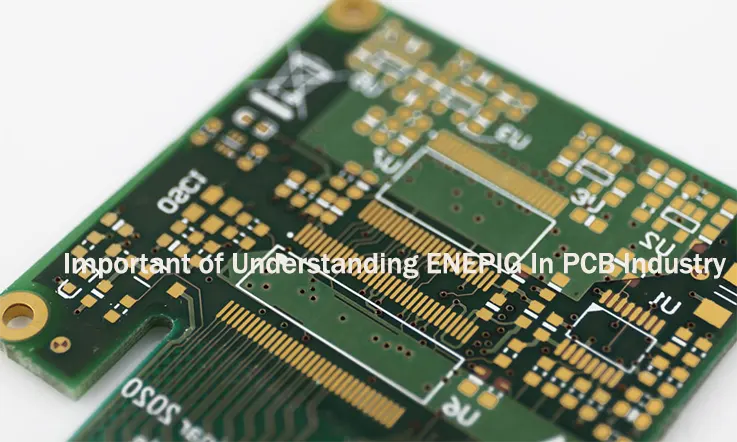
Printed circuit boards (PCBs) play a critical role in electronic devices, and it is essential that they have a long shelf life to maximize their durability. One of the most effective ways to achieve this is by applying a protective surface finish to shield the copper layer from environmental factors that can compromise its performance. ENEPIG is a technology utilized in the PCB fabrication process to create a protective finish that prevents copper oxidation and other forms of corrosion, thereby extending the lifespan of the PCB.
Therefore, ENEPIG PCB is a type of surface finish used in the manufacturing of printed circuit boards (PCBs). It stands for Electroless Nickel Electroless Palladium Immersion Gold and is known for its excellent corrosion resistance, solderability, and wire bonding capabilities. ENEPIG has become increasingly popular in recent years due to its ability to meet the stringent requirements of modern electronic devices.
In this article, we will explore the composition, manufacturing process, applications, and advantages and disadvantages of ENEPIG PCB, as well as compare it with other surface finishes commonly used in the industry.
Understanding ENEPIG
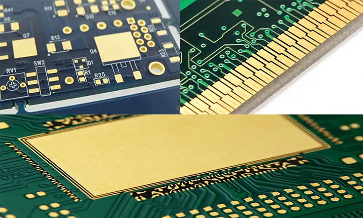
ENEPIG, or Electroless Nickel Electroless Palladium Immersion Gold, is a surface finish used in the manufacturing of printed circuit boards (PCBs). It is composed of three layers: an electroless nickel layer, an electroless palladium layer, and an immersion gold layer.
The electroless nickel layer is the first layer applied to the PCB substrate. It is applied through a chemical process that involves the deposition of nickel onto the copper surface of the PCB. This layer serves as a barrier between the copper and the outer layers of the surface finish.
The electroless palladium layer is applied on top of the electroless nickel layer. It is also deposited through a chemical process and serves as a diffusion barrier between the nickel layer and the immersion gold layer. Palladium is preferred to other metals, such as nickel or copper, as it is less prone to tarnish and provides better adhesion for the immersion gold layer.
The immersion gold layer is the outermost layer of the ENEPIG surface finish. It is deposited through an electroless immersion process and provides excellent solderability, wire bonding, and corrosion resistance. The thickness of the immersion gold layer can vary depending on the application, but it typically ranges from 0.05 to 0.2 microns.
ENEPIG is known for its excellent corrosion resistance, solderability, and wire bonding capabilities. It is also widely used in the industry due to its ability to meet the stringent requirements of modern electronic devices. However, ENEPIG is relatively expensive compared to other surface finishes and requires more processing steps, which can increase the overall cost of manufacturing PCBs.
How Does ENEPIG work?
To understand the working of ENEPIG, it is crucial to examine the four layers of metal structure that constitute the finish. The process involves the following steps:
Copper Activation
The first step of the process is selectively activating the copper layer to determine the deposition pattern of the nickel layer during electroless plating. A displacement reaction creates a catalytic copper surface on which the nickel will sit.
Electroless Nickel
Copper can react with gold, making nickel a necessary barrier layer to separate the two metals. An oxidation-reduction reaction is used to deposit the nickel onto the catalytic copper surface, creating a layer that is typically 3 to 5 microns thick.
Electroless Palladium
The palladium layer serves as another barrier layer, preventing the nickel from corroding and diffusing into the gold. It also acts as an anti-corrosion and anti-oxidation layer. Similar to the electroless nickel application, this step utilizes an electroless oxidation-reduction chemical reaction to make the nickel react with palladium. The thickness of the palladium layer can range from 0.05 to 0.1 microns, depending on the application.
Immersion Gold
The final step involves the addition of the gold layer to protect against oxidation and friction while providing low contact resistance. Gold also helps to preserve the solderability of palladium. Immersion of gold involves fully immersing the PCB while using a displacement reaction to dissolve palladium and release electrons that reduce the surrounding gold atoms. The gold ions then attach to the PCB surface, replacing some of the palladium. As a result, the finish has a gold plating layer that is typically 0.05 to 0.2 microns thick, significantly thinner than other gold plating techniques.
All in All, the ENEPIG process involves four layers of metal structure that serve as barriers and anti-corrosion/oxidation layers, ultimately resulting in a thin gold plating layer that provides excellent protection and solderability.
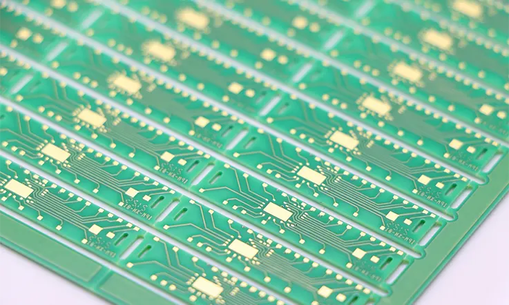
ENEPIG PCB Manufacturing Process
The ENEPIG (Electroless Nickel Electroless Palladium Immersion Gold) PCB manufacturing process involves several steps to create a surface finish that provides excellent protection and solderability. The following is a brief overview of the ENEPIG PCB manufacturing process:
Preparation of PCB substrate
The first step is to prepare the PCB substrate, which involves cleaning and degreasing the surface to remove any impurities. The substrate is then etched to remove any unwanted copper, leaving behind the desired circuit pattern.
Electroless Nickel Deposition
The next step is to deposit a layer of electroless nickel onto the substrate. This process involves immersing the PCB in a solution containing nickel ions and a reducing agent. The nickel ions are reduced and deposited onto the catalytic copper surface, creating a layer that is typically 3 to 5 microns thick.
Electroless Palladium Deposition
After the electroless nickel layer is deposited, the PCB is immersed in a palladium solution to deposit a layer of electroless palladium. This layer serves as a barrier to prevent nickel from diffusing into the gold and also provides anti-corrosion and anti-oxidation properties. The thickness of the palladium layer can range from 0.05 to 0.1 microns, depending on the application.
Immersion Gold Deposition
The final step is to immerse the PCB in a gold solution to deposit a layer of immersion gold. This layer provides excellent protection against oxidation, friction, and low contact resistance while also preserving the solderability of the palladium layer. The immersion gold layer is typically 0.03 to 0.05 microns thick.
Quality Control
Throughout the ENEPIG PCB manufacturing process, quality control measures are taken to ensure that the final product meets the desired specifications. This includes monitoring the thickness and composition of each layer, as well as performing various tests to ensure the finish’s reliability and functionality.
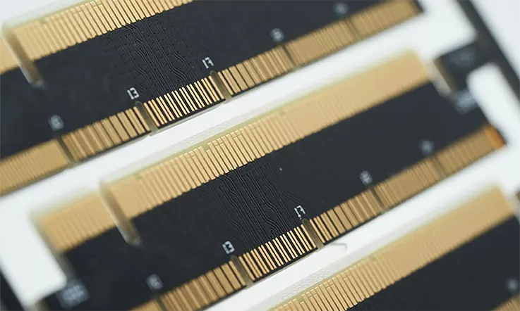
Applications of ENEPIG PCB
ENEPIG (Electroless Nickel Electroless Palladium Immersion Gold) PCB is a popular surface finish used in the electronics industry due to its excellent properties such as high corrosion resistance, good solderability, and wire bonding compatibility. It finds its use in various applications, including:
Consumer Electronics: ENEPIG PCB is commonly used in consumer electronic products such as smartphones, tablets, and laptops due to its high reliability, durability, and excellent electrical properties.
Automotive Industry: ENEPIG PCB is widely used in the automotive industry due to its high resistance to corrosion, humidity, and thermal cycling. It is used in various applications such as engine control units, anti-lock braking systems, and airbag control modules.
Aerospace Industry: ENEPIG PCB is used in the aerospace industry due to its high reliability and durability in extreme conditions. It is used in applications such as flight control systems, navigation systems, and communication systems.
Medical Devices: ENEPIG PCB is used in medical devices due to its biocompatibility, high reliability, and excellent electrical properties. It is used in applications such as implantable devices, diagnostic equipment, and monitoring systems.
Comparison of ENEPIG with Other Surface Finishes
There are different types of surface finishes used in printed circuit boards (PCBs), and each has its advantages and disadvantages. Here is a comparison of ENEPIG with other commonly used PCB finishes:
HASL (Hot Air Solder Leveling): HASL is a cost-effective surface finish that provides good solderability. However, it has limitations in terms of surface planarity, shelf life, and potential for thermal shock.
ENIG (Electroless Nickel Immersion Gold): ENIG is a popular surface finish that provides excellent solderability, corrosion resistance, and wire bonding compatibility. However, it has limitations in terms of thickness control, brittleness, and cost.
OSP (Organic Solderability Preservative): OSP is a surface finish that provides good solderability and planarity. However, it has limitations in terms of shelf life, thermal resistance, and compatibility with lead-free solders.
ENIPIG:While the acronyms ENEPIG and ENIPIG may look similar, the two surface finishes have different processes to apply the barrier layer. ENEPIG uses an electroless palladium process, while ENIPIG uses an immersion palladium process. Despite having the same layering, ENIPIG is also a versatile finish.
However, immersion palladium has some drawbacks compared to electroless plating. It can limit the thickness of the new layer and create poor adhesion, which gives ENEPIG an edge.
In comparison, ENEPIG provides a balance of excellent properties such as high corrosion resistance, good solderability, and wire bonding compatibility. It also has advantages over other finishes such as:
● Thicker nickel and palladium layers provide better protection against corrosion and diffusion.
● Lower gold thickness reduces the risk of solder joint embrittlement
● Compatibility with lead-free and eutectic solders.
● Suitable for fine-pitch applications.
However, ENEPIG has some limitations, such as higher cost compared to other finishes and the need for careful control of the plating process.
In summary, ENEPIG is a surface finish that offers a balance of excellent properties and is suitable for a wide range of applications. While other finishes may have advantages in certain areas, ENEPIG is a popular choice due to its overall performance.
Comparison of Final Finish Performance
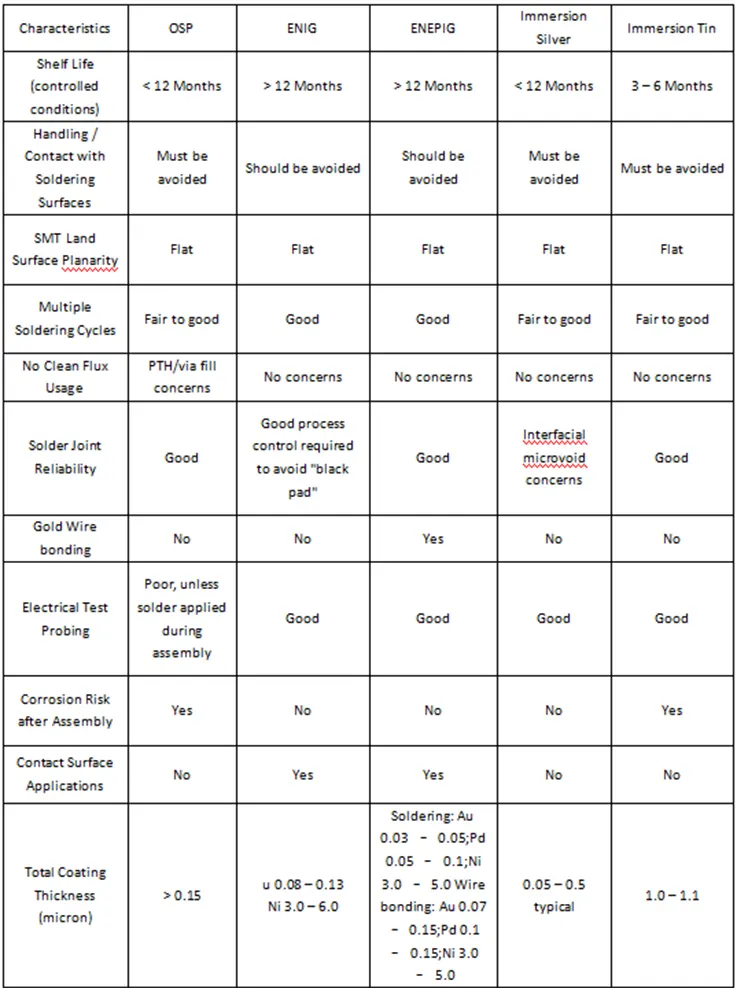
Upon evaluating the ultimate finishing outcomes across various assembly techniques, it is discernible that Electroless Nickel Electroless Palladium Immersion Gold (ENEPIG) is a fitting choice for an extensive spectrum of assembly prerequisites.
Things To Be Wary About With ENEPIG
Despite its many advantages, the ENEPIG (Electroless Nickel Electroless Palladium Immersion Gold) process has some drawbacks that experts have extensively studied. These include cost, reliability, and fractures.
The cost of the ENEPIG process can be relatively high, particularly due to the high cost of gold. Although palladium prices have decreased in recent years, gold prices have remained high, making the process somewhat expensive. Additionally, the process can be wasteful if gold wire bonding or lead-free coating is not required.
Reliability is also a concern with ENEPIG, particularly with lead and tin bonding. Due to the distribution of palladium and the presence of copper, bonding with these metals may have some reliability issues. In comparison, ENIG (Electroless Nickel Immersion Gold) provides better bonding performance and reliability with these metals.
Finally, the ENEPIG process can result in a brittle surface above the nickel plating, making it more prone to fracturing. This is because the tin-palladium metallic layers form a brittle layer above the nickel plating.
In conclusion, while the ENEPIG process has many advantages, it is essential to be aware of its potential drawbacks. By understanding the limitations of the process, manufacturers can make informed decisions about whether ENEPIG is the most suitable surface finish for their specific application.
Measures to Cost-Effective Surface Finish
Upon considering the advantages and disadvantages of Electroless Nickel Immersion Gold (ENIG) and Electroless Nickel, Electroless Palladium, Immersion Gold (ENEPIG) plating methods, the latter appears to be a more promising option. However, the higher cost of ENEPIG relative to ENIG presents a notable drawback.
One of the primary issues with ENIG plating is the formation of black pads. This problem can be addressed through the implementation of an appropriate plating method. However, with an electroless gold layer in ENIG plating, detecting the presence of black pads can be difficult.
This is due to the fact that the nickel layer remains concealed until the gold layer is chemically stripped away. Additionally, a phosphorus-rich nickel layer is produced naturally upon contact with nickel and gold, as well as solder and nickel before and after soldering, respectively.
The actual causes of black pads can be attributed to poor implementation of technology, resulting in non-uniform crystal particle formation and numerous cracks. Additionally, prolonged immersion of gold can lead to corrosion and crack formation on the nickel surface.
The solder mask utilized can also impact the electroless nickel plating process. An incorrect solder mask can result in a degraded pad surface. Moreover, inadequate cross bonding and rigidity can impede the copper activation reaction. When exposed to a hot electroless nickel solution, the solder mask monomer generates hydrogen, hindering the nickel reaction and disrupting the chemical balance.
Furthermore, the solder mask present in micro vias can undergo electrochemical reactions, impeding the creation of a catalytic copper surface during the plating process.
How To Solve the Black Pad Issue
To effectively the issue of black pads, manufacturers must implement several key measures.
First, analyzing the stabilizer content of the electroless nickel solution and controlling its PH value can help prevent the formation of black pads. Additionally, it is important to prevent nickel surface corrosion when immersing it in gold.
Fortunately, new immersion gold technology has emerged as a viable solution to this problem, as it effectively reduces plating costs while minimizing corrosion on the nickel surface. This is achieved by creating a more neutral pH range of 7.0 to 7.2, which helps to minimize corrosion. Furthermore, the new technology utilizes a lower gold content, thereby reducing the cost of raw materials and minimizing its influence on the nickel surface.
Another key benefit of this new technology is that it produces a nickel film with a columnar structure, which means that micro-cracks can only form on the surface. This further helps to minimize the risk of black pad formation and ensures that the plating process is more reliable and effective.
Conclusion
The ENEPIG (Electroless Nickel Electroless Palladium Immersion Gold) process is a surface finish used in printed circuit board (PCB) manufacturing. It involves the deposition of four layers of metals, starting with copper activation, electroless nickel deposition, electroless palladium deposition, and immersion gold deposition. Each layer serves a specific purpose, such as preventing corrosion, diffusing metals, and providing low contact resistance.
The advantages of ENEPIG include its ability to withstand thermal shock, excellent solderability, and low contact resistance. It is also suitable for high-frequency applications and can handle multiple reflow cycles without degrading. As a result, ENEPIG is commonly used in consumer electronics, automotive, aerospace, and medical devices.
Compared to other surface finishes such as HASL, ENIG, and OSP, ENEPIG offers superior performance and reliability. It is a versatile and cost-effective solution that provides excellent results for a wide range of applications.
In a word, the ENEPIG process has become an essential surface finish in the PCB industry due to its many advantages. Its ability to enhance the performance and durability of PCBs has made it a popular choice for various applications. As technology continues to advance, it is likely that ENEPIG will remain an essential component in the manufacturing of high-quality and reliable PCBs.
In addition, If you require an ENEPIG coating on your printed circuit board (PCB) for high-performance devices in your project, we can provide you with more information regarding our services. Please do not hesitate to contact us today to learn more about how we can assist you in achieving your desired results.
Related Posts:
PCB Surface Finish& Series
3.Lead Free HASL PCB Surface Finish
4.Immersion Gold PCB Surface Finish
5.Gold Plating PCB Surface Finish
6.Immersion Silver PCB Surface Finish
7.Immersion Tin PCB Surface Finish
8.Nickel Plating PCB Surface Finish
9.Immersion Nickel PCB Surface Finish
10.Hard Gold PCB Surface Finsh