
PCBA Equipment and PCB Assembly Capabilities
JarnisTech’s ISO 9001/13485-certified PCBA facility is equipped with a range of assembly techniques, such as the technology of surface mounting (SMT) screen printers and automated optical inspection and x-ray inspection equipment. The PCB assembly team at JarnisTech is made up of highly skilled IPC-A610, and J-STD001 certified assemblers that ensure the highest standard of functionality and quality of each PCBA made. PCBs of any size or complexity can be easily manufactured.
How Can JarnisTech Help With Your Custom Project ?
Thanks to these cutting-edge assembly machines, you can be able to enjoy top-quality printed circuit boards made by JarnisTech. We offer various solutions to help you with your assembly of printed circuit boards, such as:
● RoHS Lead-free Assembly that is compliant.
● Non-RoHS assembly.
● Conformal coating.
● Prototype assembly.
● Low-volume assembly.
● Consigned assembly.
● Complete turnkey assembly.
Our entire array of assembly solutions means we are able to satisfy the PCB assembly requirements specific to your business, and, in turn, you don’t need to look for a different source to assemble the printed circuit boards. This will save time, money, and logistical headaches by doing.
You Must Know 9 PCBA Equipment
In PCB assembly, there are four main steps of SMT, also known as Surface Mount Technology assembly, using the reflow method. These include the application of paste, automation placement of components as well as soldering as well as checking (plus testing, if required). The most basic equipment needed to perform PCB assembly is:
● Solder Paste Printing machine.
● Solder Paste Inspection (SPI) machine.
● Glue Dispensing Machine.
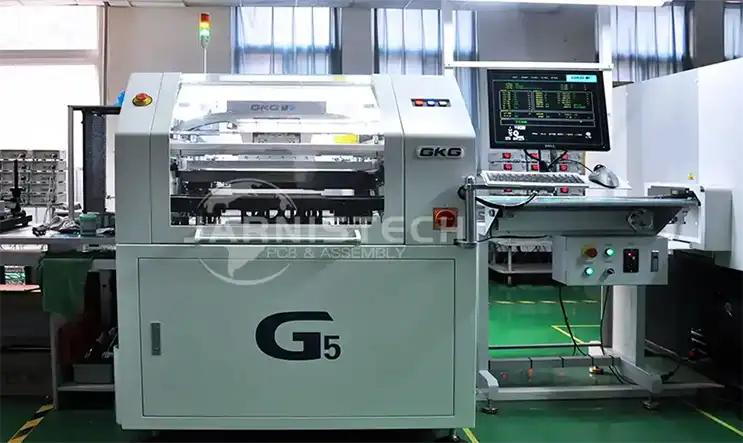
● Pick-and-Place machine.
● Reflow Soldering Machine.
● Wave Soldering Machine (for the by-hole component).
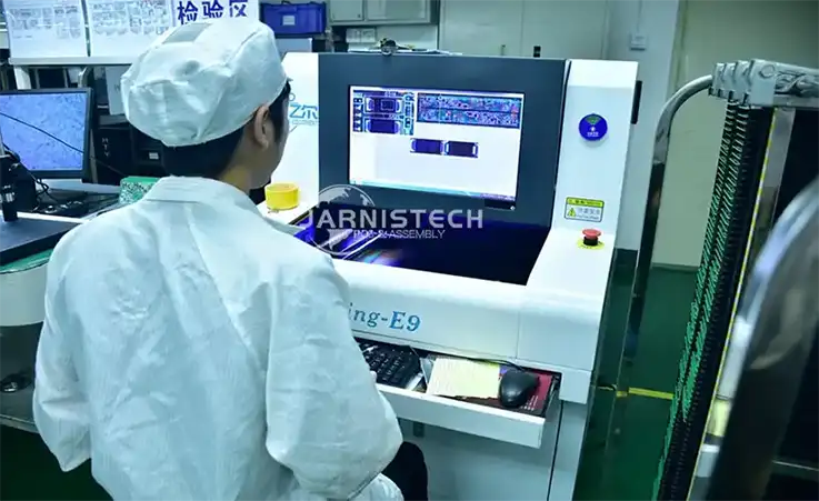
● Automated Optical Inspection (AOI) machine.
● In-Circuit Test (ICT) Fixture.
● Functional Validation Test (FVT) Fixture.
Stage 1: Paste Application
Solder Paste Printing Machine
The main function of the machine is to print the solder paste onto the PCB. It is able to be used for reflow soldering or wave soldering. The principal components of this machine comprise an extruder and a solder paste pump and a dispensing head.
The solder paste that is extruded by the extruder is then pumped through the pump before being dispensed onto the printed circuit board using the head that dispenses it.
The solder paste needs to be delivered with accuracy so that there are no dry spots or excessive solder remains on the board. This machine is also employed to print other materials like epoxy resin and electrically conductive ink.
Solder Paste Inspection (SPI) Machine
The SPI machine can be used to examine solder paste for any defects like missing or excessive tin, irregularity in the paste solder, and the color of the paste varies between different places in the PCB.
The machine also can determine the existence of particles within the paste, as well as particles that could be present on the pad of the die. In addition to optical microscopes, the SPI machine can also be used with scanning electron microscopes.
Stage 2: Automated Component Placement
Glue Dispensing Machine
Prior to the placement of components prior to component placement, the dispensing device places dots of glue on the PCB, where parts’ body components will rest, keeping the components in position until contact leads are made. This is crucial when using wave soldering, where the power of the soldering wave can dislodge bigger components, as well as for double-sided wave or reflow soldering, to prevent components from falling off.
Pick-and-Place Machine
Pick-and-place machines are probably the most mesmerizing machines in an assembly line. As its name implies, the machine is able to pick up parts and then place them on a blank board. Traditionally, this step of the PCB assembly procedure was done manually, and humans would meticulously select and place the components using an instrument like a tweezer. However, PCB manufacturers nowadays have this procedure automated by utilizing a pick-and-place machine because machines are more precise than humans and operate all hours of the day.
Pick-and-place equipment suctions up SMT components and then places them precisely in their set positions over the paste of solder. They’re thrown down at lightning speed that can reach speeds of up to 30,000 components per hour. When the machine puts components in an orderly, however, almost chaotic way watching the pick and place machines at work is definitely the most entertaining to observe!
Stage 3: Soldering
Reflow Soldering Machine
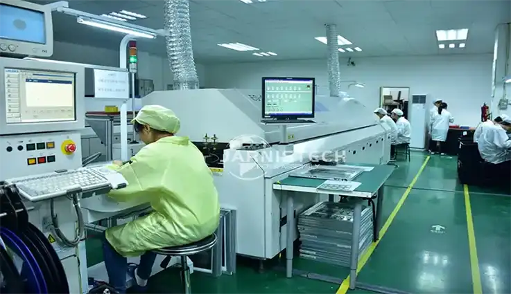
Rework soldering machines are part of the assembly process and play a crucial function in the final quality of the product.
Many who are just getting started as technicians are usually overlooked. However, it must be acknowledged that without this device, the entire process of production would stop dead in its track.
The goal of the soldering machine for rework is to create electrical connections between different components as well as other parts that are soldered together or coated with solder paste. They can also be employed for rework processes. Hence, they are called Rework stations.
Although there are a variety of kinds of these machines at present, they all operate by heating the parts by applying pressure to them at extremely high temperatures.
Technicians must be aware that when working at Rework stations, specific safety precautions and steps must be taken.
Wave Soldering Machine (For Through-hole Components)
Wave soldering machines are the most common way to solder through-hole components to PCBs. It’s among the easiest cheap, most affordable, and most flexible methods. It can be used to produce a large capacity and can be used with various technology and materials.
In wave soldering machines, molten solder flows continuously over the components when they are passed through a temperature-controlled oven.
A wave soldering machine is designed for high-throughput environments in mass manufacturing. They should be strong sufficient to handle boards that have multiple components that need to be soldered simultaneously.
It means that the majority of wave soldering equipment is designed for boards that are between 1in2 and 2in2 and have a maximum height of 0.0185in or 4 mm above the board’s surface after it goes into the oven.
By adjusting its temperature profile, a wave soldering machine can be used to solder through-hole or surface mount devices. The massive machines have two temperature zones, one to solder to the leads of the through-hole component as well as another one for the soldering of the body of the device.
Wave soldering also offers distinct advantages:
The circuit board is equipped with an extremely short contact, with high-temperature soldering, which may lower the rate of warpage of the board.
The high efficiency of the solder on the wave soldering equipment is beneficial to increasing the performance of joints soldered by it.
Stage 4: Inspection
Automated Optical Inspection (AOI)
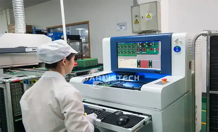
Once the boards are complete, they can be put to the test and inspected. Due to the increasing complexity of PCB boards, automated optical inspection is more crucial than ever before. Although it is still possible to focus and identify errors using your eyes, Manual inspection is not efficient for mass production because the workers become tired, and errors can be easily missed. Testing PCBAs is a vital stage in PCBA production to prevent costly re-manufacturing costs and the waste of materials. AOI systems are used to spot problems before they occur during the production process and permit processes to be improved or specific boards to be repaired.
Utilizing optical techniques to identify imperfections, AOI systems can perform checks that are previously carried out manually, however, with higher speed and precision. The AOI camera uses high-definition technology to take pictures of the surfaces of the board and create an image to analyze.
This image is examined against images of an appropriate reference board to find a variety of imperfections, from defective or missing components to scratches and shorts.
In-circuit Test (ICT) Fixture
ICT fixtures can be used for testing PCBs once they’ve been made. The fixture is connected to the PCB via an electrical power supply like that used in the majority of electronic consumer products, like your laptop computer or phone charger, for instance. It has an indicator light to show when the board is powered up.
When the board is powered on, the light will blink. You can then check whether all your components are operating properly and also if any of the traces on the board are shorting out.
It is essential to use an ICT fixture for testing boards using components mounted on surfaces as it decreases the number of external connections needed.
Functional Validation Test (FVT )
Functional Validation Testing (FVT) is the last step to provide the decision to go or not on PCBs that have been completed prior to when they are sent out for shipping. At this point, we’re no longer simply testing for physical imperfections such as tombstones or solder bridges. Instead, the software has been loaded, and we’re testing whether the board functions in the way it is supposed to when utilized in any application that our customers may have in mind for the boards.
FVT simulates the operational environment in which the PCB is used, typically through interfacing the PCB using its connector or by using it as a test point. Functional tests vary from product to product because each PCB tested is distinct. The most popular method of testing functional includes “hot mock-ups,” which is a set-up that is designed to mimic the final product the PCB is used in. However, regardless of how the FVT is configured, they are all based on the same elements of a system: the hardware and software.
Why Is JarnisTech Printed Circuit Board Assembly Good for Your Project ?
Businesses that specialize in the design of printed circuit boards or manufacturing typically don’t perform PCB assembly all that much. Some of them offer this as an afterthought or as an additional service to that they may not dedicate many resources. That means you won’t receive the top or fastest assembly at the cost.
If you submit your boards to a firm that is specialized in the design of boards, you might find a great plan. However, you’ll have to handle the logistics and the time in bringing those boards over to the new firm to be assembled, to say nothing of the extra cost.
Choose JarnisTech, and we provide you with a one-stop service for all your PCB project. With our expertise, we can design, manufacture, and assemble your product to a high standard. You can, therefore will, save time, money, and stress without worrying about or quality of your product by having JarnisTech handle all the details for you.
Our SMT Capacity: 4 Million Points per Day
| Item | Capability |
| Single and double sided SMT/PTH | Yes |
| Large parts on both sides, BGA on both sides | Yes |
| Smallest Chips size | 0201 |
| Min BGA and Micro BGA pitch and ball counts | 0.008 in. (0.2mm) pitch, ball count greater than 1000 |
| Min Leaded parts pitch | 0.008 in. (0.2 mm) |
| Max Parts size assembly by machine | 2.2 in. x 2.2 in. x 0.6 in. |
| Assembly surface mount connectors | Yes |
| Odd form parts: LED Resistor and capacitor networks Electrolytic capacitors Variable resistors and capacitors (pots) Sockets | Yes |
| Wave soldering | Yes |
| Max PCB size | 14.5 in. x 19.5 in. |
| Min PCB Thickness | 0.02 |
| Fiducial Marks | Preferred but not required |
| PCB Finish Method: | 1.SMOBC/HASL 2.Electrolytic gold 3.Electroless gold 4.Electroless silver 5.Immersion gold 6.Immersion tin 7.OSP |
| PCB Shape | Any |
| Panelized PCB | 1.Tab routed 2.Breakaway tabs 3.V-Scored 4.Routed+ V scored |
| Inspection | 1.X-ray analysis 2.Microscope to 20X |
| Rework | 1.BGA removal and replacement station 2.SMT IR rework station 3.Thru-hole rework station |
| Min IC Pitch | 0.2MM |
| solder paster printer | 0.2MM |
| POP Manufacturing capability | POP *3F |
For a quote, please send your PCB file and BOM list to [email protected]. We welcome partial or full PCB assembly.
JarnisTech has top-Of-the-line PCB assembly equipment that can help you today !
We might have a hard time believing we can achieve all of this. However, we have many satisfied customers who are pleased to support our assertions.
For more information on the ways JarnisTech and our trusted PCB assembly machine can assist you with all of your printed circuit board requirements, get in touch with us now. For a cost estimate for PCB Assembly for your current project, send your details to us by pressing the link below. We’ll contact the client with an estimation of the PCB assembly cost within one working day.
Summary
Yes, the PCB manufacturing process is critical. Therefore, you must choose a the strength company to work with, and JarnisTech is such a company, with the most modern PCB and PCBA equipment, that can meet the various specifications of PCB assembly and ensure efficient production. In addition, to ensure high-quality PCBA components, we will test the design validity of your PCB project, which may include PCB prototypes, as well as a thorough final inspection of the product.
With JarnisTech, You can’t make a mistake. We also provide the services you need at a reasonable cost. Please feel free to contact us right now.


