
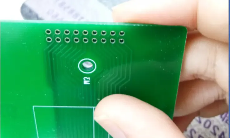
If you examine the printed circuit boards attentively (PCB). On the PCB boards, you will see a variety of holes of varying sizes. These PCB holes can be categorized into two types: PTH (Plating Through Hole) and NPTH (Non-Plating Through Hole) (Non Plating Through Hole). The simplest approach to distinguish between PTH (Plating Through Hole) and NPTH (Non-Plating Through Hole) in PCB is to examine the borehole wall for indications of plating.
During the manufacture of PCBs, Through Holes are holes that are drilled into a PCB from the top and continue all the way through to the bottom. These holes can be plated (PTH) or non-plated (NPTH). Plated (PTH) or non-plated components can be found on a printed circuit board (PCB) or flexible printed circuit (FPC) (NPTH). By using plated through holes, there is either a conductive path from one side of the board to the other, or there is no conductive path at all.
Plated Through Hole (PTH) :Definition
Both the top and bottom layers of a PTH will always feature a copper pad that extends all the way to the hole’s rim. Pads having a diameter equal to that of the PTH’s inner diameter may also be present in the inner layers surrounding the PTH, depending on the application. This is a crucial criterion for all plated through holes, since it assures that the copper barrel on the hole wall will make a good electrical connection to all the pads during the electroplating process.
When designing a circuit for a PCB, the designer needs to create a pad that has a diameter that is at least 12 mils greater than the diameter of the hole. This is necessary in order to satisfy the aforementioned criterion. Following drilling of the hole, this will result in a pad having a minimum width of 6 mil. If the PTH is in the shape of a slot, the designer needs to develop a pad that will leave a minimum width of 6 mil of copper surrounding the slot. The majority of PCB design programs will automatically apply a solder stop mask that is appropriate to the pad that is designed.
Plated Through Hole (PTH): Use
PTH refers to a metallic hole. PTH holes typically serve two purposes on circuit boards. One is for welding the legs of standard DIP components. So that the pieces can be removed, the diameter of these holes must be bigger than the diameter of the welding legs. Insert it in the hole.
Another type of relatively small PTH that is typically referred to as a via is utilized to connect and conduct the copper foil circuit between two or more layers of the PCB. As a printed circuit board (PCB) is constructed of numerous layers of copper foil, it is collected by stacking, and an insulating layer is applied between each layer of copper foil, so that the copper foil layers are unable to communicate with each other. Due to the fact that the signal connection is via via, this feature is sometimes referred to as “Plated Through Holes.”
Non-Plated Through Hole (NPTH): Definition
Considering the above description of PTH, Non-Plating Through Holes adhere to the same rules. The fundamental distinction is that the interior surfaces of the holes are not plated with conductive substances. An NPTH does not serve the same functions as a PTH because it cannot conduct electricity. The design specifications of a circuit board will indicate whether a through-hole requires plating.
Even when there is no connection, an NPTH may still have pads on either side in some circumstances. However, this does not indicate a connection. Pads serve as guidance for the placement of NPTHs; nevertheless, the majority of NPTHs do not need pads at all and instead appear on the circuit board as simple holes. Because confusing an NPTH for a PTH can lead to problems with the circuit pathing on a printed circuit board, designers have to make sure they correctly set an NPTH regardless of whether the assembly is done manually or automatically. If a PTH is used in a situation where an NPTH is required, the charge will be misdirected or distributed too thinly, which will either cause the charge to be weakened or produce bridging, which will lead to short circuits.
Non-Plated Through Hole (NPTH): Use
The abbreviation NPTH refers to a non-metallized hole. The hole does not contain any copper. The top and bottom layers of the PCB are electrically isolated through holes. Similar holes have blind and buried holes. PTH or NPTH through holes can be utilized according on the requirements. For instance, holes used to connect wires require PTH, but holes used for fastening purposes, such as screw holes, can be NPTH.
In a word, the primary purpose of an NPTH is to serve as a mounting guide for a printed circuit board (PCB). NPTH typically offers a channel through which the board can be secured with bolts or screws. In certain instances, wires or pins are threaded through them. In both cases, components threaded through the circuitry of the board must not interfere. This will be possible due to the unplated nature of the NPTH.
Adding PTH&NPTH to a Boards Design: Rules
At separate phases of the manufacturing process, the two types of through holes are added to the board. Before to drilling, there are a few guidelines rules to keep in mind:
The Through Holes: When to Driled?
Before beginning the process of electroless plating, a design that needs a plating through hole should always have the board substrate drilled. In this manner, when the traces are filled and the conductive material is set, it will coat the inside of the holes, so making a solid circuit. For Non-Plating Through Holes, they must be drilled after plating has been completed. By to do, the hole will remain clear of plating material.
Consider Hole Width
The following are the parameters that define any through hole as standard:
● 0.006” minimum finished hole size for PTH.
● 0.004” minimum annular ring size for NPTH.
● 0.006” minimum finished hole size for NPTH.
● 0.009” minimum edge-to-edge clearance from any surface element for PTH.
● 0.005” minimum edge-to-edge clearance from any surface element for NPTH.
In order to avoid interference from other components, these are designed to provide proper coverage to each through hole while also providing sufficient distance from other components. In addition, take into consideration the size of any plugs or bolts that will be supplied via an NPTH in order to provide enough surface clearance.
The through-hole technology is not as straightforward as just drilling a hole through a printed circuit board (PCB). Each hole on the printed circuit board (PCB) needs to have a function, or else it runs the risk of becoming an unnecessary expense for the production process or a threat to the board’s ability to retain its structural integrity. When designing through holes, it is important to give careful consideration to their function and to make certain that manufacturers completely comprehend what that function is.
Through-Hole Technology
Through-hole technology (THT), also known as through-hole assembly, is a mounting scheme for electronic components that is used in PCB assembly. This mounting scheme involves the use of leads on the components, which are inserted into holes drilled in PCBs and soldered to pads on the opposite side either manually (hand placement) or using automated insertion mount machines.
Earlier methods of assembling electronic components, such as point-to-point manufacturing, were almost entirely supplanted by THT. Every component on a standard printed circuit board (PCB) was a through-hole component between the time of the second generation of computers in the 1950s and the time that surface-mount technology (SMT) became widespread in the late 1980s. Printed circuit boards (PCBs) first included tracks printed solely on one side, then both sides, and eventually multilayer boards came into use.
In order for the components to make contact with the necessary conducting layers, the through-holes were converted into plated-through holes, abbreviated PTH for short. Plated-through holes are no longer necessary for creating component connections when using SMT boards; nevertheless, they are still needed for making interconnections between the layers and are more commonly referred to as vias when serving in this capacity.
THT is still used today, especially on boards that require thru-hole components such as antennas, DC jacks, and wires, despite the fact that surface mount technology has surpassed it as the leading technology for the manufacturing of PCB assembly.
The Reason Why the Use of NPTH Fell ?
Non-Plating-Through-Hole Printed Circuit Boards have basic features that are drilled or machined through the circuit board. Due to the absence of copper plating on the components, the hole possesses no electrical qualities. While PCBs had copper traces printed on only one side, NPTHs were prevalent, but as multilayer PCBs became the norm, NPTHs lost favor. Currently, they are predominantly utilized as mounting holes to permit screws or other fasteners to pass through PCBs.
The Reason Why SMT is Popular Now ?
Through-holes have been largely phased out in favor of SMT Surface Mount Technology in recent years as a result of its lower manufacturing costs, more automation, and overall improvement in quality.
The electrical component that is mounted on a surface-mount technology is referred to as a surface-mount device (SMD). In surface-mount technology (SMT), they are frequently used as capacitors and resistors. While SMDs may be manufactured to be very small, SMT is able to carry a great deal more components on a substrate that is the same size.
PTH Vs. NPTH
Pads on a printed circuit board are the exposed metals on the substrate where component leads are soldered. Several pads are utilized simultaneously to generate a land pattern (component footprint) on the printed circuit board. Pads can be either through-hole or surface mount. If the pad of a hole has copper and the solder stop mask, the hole is classified as PTH. This should be a minimum of 6 mils wide and larger than the hole/slot it is overlaying.
NPTH refers to holes in which the copper size of the pad is either less than the size of the hole itself or there is no copper at all. In addition, there will be a six mil gap between the copper and the hole, even if the copper is overlay or larger than the hole.
The production of NPTH is easier, which results in a shorter turnaround time. The majority of the time, but not always, these holes serve the purpose of Tooling/Mounting holes, which are utilized to fasten the PCB to its operating location.
In addition, Plated-through-hole printed circuit boards (PCBs) come at a premium price compared to their non-plated-through-hole counterparts. In addition, printed circuit boards that use PTH technology are typically more compact than printed circuit boards that use NPTH technology.
Land Patterns & Component Footprints
The printed circuit boards’ circuits, which are responsible for interconnecting the various electronic components, are the most essential component. Components are soldered to printed circuit boards (PCBs) the vast majority of the time; nevertheless, in order for the soldering process to be successful, the conditions must be suitable. It is necessary for the leads of a component to have a reliable electrical and mechanical connection to the etched copper traces in order for the component to function properly.
In addition, each component must have its own footprint or land pattern. This footprint is how the pads are placed in through-hole technology or surface-mount technology, and it is used to attach and electrically connect components to the PCB. The land pattern of a component consists of etched copper characteristics that correspond to the component’s leads. These land patterns are typically created somewhat larger than component leads to provide space for soldering.
Because the majority of PCBs are double sided or multi-layered, the plating of the Through Holes is required so that components can link with each other and with required layers in the board. This is because most PCBs are made up of many layers.
PTH Production: Advantages
PTH assembly produces substantially stronger mechanical connections between components and the circuit board than surface-mount techniques. Instead of replacing the complete circuit board, faulty connections can be rectified manually, one at a time. However, the cost of PTH PCBs is higher.
PTH assembly is utilized for large components, such as large package semiconductors that require strong mounting strength to endure high stresses, or in electrolytic capacitors used in electronic modules, power supply, and LED assembly applications.
Since investors require less equipment, cheaper prices, fewer manufacturing processes, and larger profit margins, process and design engineers have developed a two-phase approach that combines through-hole and surface mount techniques.
Lowering Through Hole PCB Cost
Drilling a printed circuit board (PCB) adds an additional fee on top of the cost of the board itself. The total cost of the board is determined not only by the number of holes on the board but also by the size of those holes, the size of the annular rings surrounding the holes, and the design of the holes. The following are some suggestions that can be used to bring down the price of a printed circuit board that has through holes:
Use Lower Hole density
To get a higher hole density, the board must be drilled with more holes on each square centimeter of its surface. In addition to making the PCB less robust mechanically, this also lengthens the amount of time required for drilling. This causes an increase in the amount of time required to fabricate the PCB, which in turn raises its price. By reducing the hole density, it may be possible to bring the price of the printed circuit board down.
Use Larger Diameter Holes
It costs more to drill holes that are smaller in diameter. There is a requirement for a higher level of precision, and if drill bits break more frequently, not only will the overall cost increase, but the fabrication process will also take longer. Getting in touch with the PCB manufacturer is the most effective way to get the true price of a board that has holes of very small diameters. The majority of PCB suppliers tack on an additional fee for holes with widths ranging from 0.15 mm to 0.3 mm.
Use Large Annular Rings
Drilling with greater precision is required whenever the annular ring that surrounds the hole is of a smaller diameter. If the centering of the drill isn’t done precisely, the annular ring around the hole might not be able to keep its consistent appearance. The utilization of a sizable annular ring eliminates the need to be concerned about this. Nevertheless, this decreases the amount of space available on the printed circuit board (PCB) for routing traces, which may necessitate an increase in the size of the PCB.
Contact us if you need more information about through-hole technology and PTH assembly, or if you need assistance determining the expenses associated with PTH and NPTH manufacture. Your questions will be responded to as quickly as possible.
Final Words
Through-hole technology was originally required for the production of multilayered circuit boards; but, thanks to advances in manufacturing methods, such as those utilized by JarnisTech, have drastically reduced their utilization. Although though printed circuit boards can still feature non-plated through holes and plated through holes, the quantity of each type of hole on the board is limited by the application it will be used for.
Staying in contact with your printed circuit board (PCB) provider (JarnisTech) to verify the minimum requirements on through holes and others for a standard PCB can bring you savings in terms of the costs associated with PCB manufacture and assembly.
Related Posts:
1. What Is PCB Etching and How to Make a perfect PCB Etching?
2. The Best PCB Panelization Guide
3. The Importance of 3D Printed PCBs in Modern Electronics Production
4. Understanding PCB Delamination: A Comprehensive Guide
5. The Best Backplane Printed Circuit Boards Factory
6. An Overview of Through-hole Technology (THT)
7. Detail Talk Surface Mount Technology
8. PCB Clone : Copy Your Printed Circuit Board
9. PCB Drilling: Definition, Technology Types and Process
10. Castellation PCB Fabrication: Castellated Hole (Plated Half Hole) Technologys Why So Important


