The choice of materials plays a pivotal role in the design and performance of RF PCBs. RF (Radio Frequency) circuits operate at high frequencies, demanding specific material properties to ensure optimal signal integrity, impedance control, and overall system performance.
In this informative article, we aim to offer a thorough and all-encompassing set of instructions for the design of RF printed circuit boards (PCBs). Our guidelines will cover crucial aspects such as layout considerations, stackup configuration, material selection, simulations, fabrication techniques, and assembly processes. Moreover, we will conduct a comprehensive evaluation of various microwave substrate materials commonly employed in RF board manufacturing. Among the materials to be assessed are well-known options like Rogers, Taconic, Isola, and Arlon laminates.
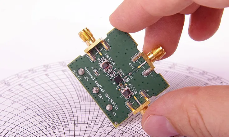
Introduction of RF Circuit Boards
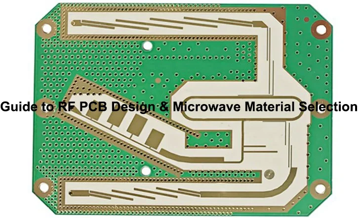
Radio frequency (RF) circuit boards also referred to as RF circuit boards are made printed circuit boards intended for use in frequencies spanning from 30 kHz to 100 GHz. They play a role in a wide range of high frequency applications, like wireless communication, radar systems, broadcasting and other electronic setups that depend on consistent signal transmission and accuracy.
The design and construction of RF circuit boards require specific expertise and considerations due to the unique challenges posed by high-frequency signals. These challenges include signal loss, impedance matching, electromagnetic interference (EMI), and signal integrity issues. Therefore, RF circuit board design involves careful attention to layout, stackup design, material selection, simulations, fabrication techniques, and assembly processes.
Layout considerations for RF circuit boards involve optimizing the placement and routing of components to minimize signal loss and interference. The stackup design involves selecting the appropriate number and arrangement of PCB layers, as well as the placement of ground and power planes to ensure controlled impedance and minimize EMI.
Material selection is a critical aspect of RF circuit board design. Microwave substrate materials with specific dielectric properties and low signal loss are chosen to meet the demanding requirements of high-frequency applications. Popular options for RF circuit boards include Rogers, Taconic, Isola, and Arlon laminates, each offering unique characteristics and performance advantages.
Simulations are commonly employed during the design phase to analyze and optimize the RF circuit board’s performance. Tools such as electromagnetic simulation software help predict signal behavior, identify potential issues, and fine-tune the design for optimal performance.
Fabrication and assembly processes for RF circuit boards require specialized techniques to ensure precise manufacturing and reliable operation. These processes may include controlled impedance manufacturing, high-precision drilling, and careful soldering techniques to maintain signal integrity and minimize losses.
Therefore, RF circuit boards are vital components in high-frequency electronic systems, and their design requires specialized knowledge and expertise. By following comprehensive guidelines and considering factors such as layout, stackup design, material selection, simulations, fabrication, and assembly processes, engineers can achieve the desired signal integrity, transmission characteristics, and reliability in RF applications.
RF PCB Design Guidelines
RF PCB Design Guidelines process:
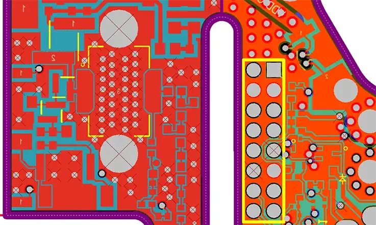
1.Board Stackup Design:
Carefully design the PCB stackup to achieve controlled impedance, minimize signal loss, and reduce electromagnetic interference. Consider the number and arrangement of layers, placement of power and ground planes, and dielectric materials.
2.Trace Routing:
Pay attention to trace widths, spacing, and impedance matching to maintain signal integrity. Use transmission line techniques such as microstrip or stripline routing for high-frequency signals.
3.Components Placement:
To enhance performance arrange the components strategically to shorten signal paths decrease interference and maintain temperature control. Keep frequency parts in close proximity and limit the number of vias used.
4.Grounding Design:
Implement a solid ground plane to provide a low-impedance return path for RF signals. Use stitching vias to connect ground planes and minimize ground loops.
5.Layer Strategy:
Determine the optimal layer arrangement based on the complexity of the RF circuit. Consider separating sensitive analog and digital signals onto different layers to minimize interference.
6.Passive Integration:
When setting up your components try to place elements like capacitors and inductors near the active components, for better performance and reduced interference.
7.Transitions and Terminations:
Use appropriate transition techniques, such as transmission line matching, to ensure efficient signal transfer between different impedance domains. Terminate unused transmission lines to minimize reflections.
8.Shielding and Partitions:
Employ shielding techniques, such as metal enclosures or copper shielding, to isolate sensitive RF components from external electromagnetic interference. Use partitions to separate different functional blocks on the PCB.
9.Simulations:
Utilize electromagnetic simulation software to analyze and optimize the RF PCB design. Perform signal integrity, power integrity, and electromagnetic interference (EMI) simulations to identify and mitigate potential issues.
10.Materials:
Choose high-quality microwave substrate materials with low dielectric loss, high thermal conductivity, and appropriate dielectric constant for the desired frequency range. Popular options include Rogers, Taconic, Isola, and Arlon laminates.
By following these guidelines, engineers can design RF PCBs that meet the stringent requirements of high-frequency applications, ensuring optimal signal integrity, transmission characteristics, and reliability.
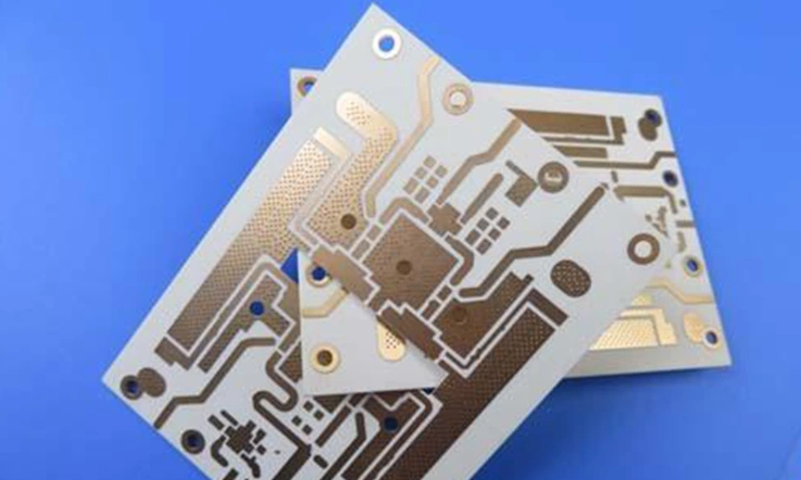
Microwave Laminates Materials for RF PCBs
RF printed circuit board (PCB) substrates must possess two crucial characteristics: a consistent dielectric constant and a minimal loss tangent across the operating frequency spectrum. To achieve optimal performance, several microwave laminate materials are commonly utilized in the industry.
Here’s microwave laminate materials offered by Park Electrochemical, Rogers Corporation, Isola, Taconic, and Arlon:
Park Electrochemical:
Park Electrochemical provides a range of microwave laminate materials under their NelsonicTM brand. These laminates are designed for high-frequency applications and include options such as:
●N9000-13EP: A tight tolerance woven glass reinforced substrate.
●N9000-13SI: A filled ceramic PTFE composite material.
●N9120-4: A high-frequency laminate with PPS thermoplastic reinforcement
Rogers Corporation:
Rogers Corporation is a well-known manufacturer of printed circuit materials for high-frequency applications. They offer various microwave laminates, including:
●RO3003TM: A glass microfiber filled PTFE substrate with low dielectric constant (Dk) and dissipation factor (Df).
●RO3003TM: A glass microfiber filled PTFE substrate with low dielectric constant (Dk) and dissipation factor (Df).
●RO4350BTM: A woven glass reinforced, ceramic-filled laminate with a high dielectric constant.
●RT/duroid® 6002: A ceramic-filled PTFE material with tight Dk and Df tolerances.
●RO4835TM: A glass microfiber filled, ceramically loaded laminate.
●TMM® 10i: A woven glass reinforced, ceramic-filled PTFE material.
Isola:
Isola specializes in high-performance copper clad laminates, including materials suitable for RF applications. Some of their microwave laminates are:
●IS680: A low Dk glass weave reinforced laminate.
●FR408HR: A high-performance FR-4 material with tight dielectric tolerance.
●P96: A high thermal reliability FR4 material.
●Getek®: Glass microfiber reinforced fluoropolymer substrates.
●ISOLA Astra MT77: A composite material designed for broadband applications.
Taconic:
Taconic offers a broad range of RF laminates suitable for microwave applications. Their microwave laminate materials include:
●TLY-5TM: A low-loss thermoset laminate for analog circuits.
●TLC-30TM: A low Dk glass microfiber PTFE composite.
●RF-35TM: A ceramic-filled PTFE material for broadband applications.
●RF-60TM: A thin film ceramic-filled fluoropolymer laminate.
●TacPreg®: Low-loss thermoset prepregs available in various Dk.
Arlon:
Arlon specializes in high-performance laminates for microwave and thermal management applications. Some of their microwave laminate materials are:
●CLTE-XT: A low Dk glass reinforced hydrocarbon ceramic laminate.
●CLTE-AT: A glass reinforced PTFE composite material.
●55NT: A non-PTFE, thermoset microwave substrate.
●25N: An economical woven glass reinforced laminate.
These manufacturers offer a variety of microwave laminate materials suitable for RF PCBs, each with its own unique properties, such as dielectric constant, dissipation factor, and thermal characteristics. Engineers can choose the most appropriate material based on their specific design requirements and performance considerations.
Manufacturing and Assembly Considerations For RF PCB
Fabricating RF PCBs requires specialized expertise and adherence to specific processes to ensure controlled impedance, tolerances, surface finishes, and reliability. Here are some key guidelines for RF board fabrication and assembly:
1. Maintain excellent impedance tolerance of ±5% or better: Precise control of impedance is crucial for RF circuits to ensure proper signal propagation. It is important to meet or exceed the specified impedance values with a tight tolerance.
2. Use industry standard IPC laminate test vehicles for validation: IPC (Association Connecting Electronics Industries) provides standard test vehicles that can be used to validate the performance of the fabricated PCBs. These test vehicles help ensure that the PCBs meet the required specifications.
3. Implement controlled environment conditions – temperature, humidity: A controlled environment with stable temperature and humidity levels is essential during the fabrication and assembly processes. Fluctuations in temperature and humidity can impact the material properties and lead to variations in circuit performance.
4. Confirm surface roughness, copper thickness, dielectric values: Surface roughness, copper thickness, and dielectric values are critical parameters that affect signal integrity and impedance control. These parameters should be carefully monitored and confirmed to meet the design requirements.
5. Utilize impedance controlled bondply innerlayer materials: Bondply materials with controlled impedance properties should be used for inner layers to ensure consistent impedance throughout the PCB. These materials help maintain signal integrity and minimize impedance variations.
6. Employ sequential lamination process: Sequential lamination involves building up the PCB layer by layer, allowing for precise control of the dielectric thickness and impedance. This process helps achieve the desired impedance characteristics.
7. Implement rigorous quality inspection procedures: Quality inspection procedures, including visual inspection, dimensional checks, and electrical testing, should be implemented at various stages of the fabrication and assembly processes. This ensures that the PCBs meet the required quality standards.
8. Verify plating quality – surface, hole wall, via filling: Plating quality is critical for reliable RF PCBs. The plating on the PCB surface, hole walls, and vias should be carefully inspected to ensure proper thickness, coverage, and adhesion.
9. Use automated optical inspection (AOI): Automated optical inspection systems can detect defects such as missing components, misalignments, soldering issues, and surface abnormalities. AOI helps ensure the quality and reliability of the assembled RF PCBs.
10. Perform electrical testing like time domain reflectometry: Electrical testing, such as time domain reflectometry (TDR), can be used to verify the impedance characteristics and identify any signal integrity issues. TDR helps detect impedance mismatches, signal reflections, and other anomalies.
11. Include fixture and jig design for repeatable assembly: Fixtures and jigs should be designed and used during the assembly process to ensure repeatable and accurate placement of components. This helps maintain consistency and reliability in the assembly process.
12. Execute thermal profiling for soldering processes: Thermal profiling involves monitoring and controlling the temperature profile during the soldering process. It ensures that the solder joints are properly formed and provides reliable connections between components and the PCB.
13. Conduct shock and vibration testing on assemblies: RF PCB assemblies should undergo shock and vibration testing to ensure their robustness and reliability in real-world operating conditions. This testing helps identify potential weaknesses and design flaws that could impact performance.
By following these guidelines, manufacturers can produce high-quality RF PCBs that meet the stringent requirements of controlled impedance, tolerances, surface finishes, and reliability for RF applications.
Frequently Asked Questions
Interface Design Considerations for RF PCBs
When creating RF (Radio Frequency) PCBs (Printed Circuit Boards) it’s important to address various interface design challenges to achieve the best performance. Here are a few important factors to keep in mind:
●Impedance Matching
●Signal Integrity
●Electromagnetic Interference (EMI)
●RF Trace Routing
●Grounding
●Thermal Management
●Thermal Management
●Component Placement
●Manufacturing and Assembly
These are some of the key interface design issues that need careful consideration when designing RF PCBs. It’s important to consult RF design guidelines, standards, and experienced RF engineers to ensure optimal performance and reliability.
How Are Materials Select for RF Printed Circuit Board?
When picking out materials for RF (Radio Frequency) PCBs (Printed Circuit Boards) it’s important to take into account factors to guarantee top notch performance at high frequencies. Here are a few essential things to think about when selecting materials, for RF PCBs:
●Dielectric Constant (Dk)
●Loss Tangent (Dissipation Factor)
●Thermal Properties
●RoHS Compliance
●Frequency Range
●Cost
Commonly used materials for RF PCBs include:
●FR-4 (Flame Retardant 4)
●PTFE (Polytetrafluoroethylene)
●Rogers Corporation Materials
●Ceramic-filled Materials
The material selection process involves considering the specific requirements of the RF application, balancing performance with cost, and consulting material datasheets, manufacturers, and experienced RF engineers.
Types of Manufacturing Processes for RF PCB Fabrication
The implementation of a procedural lamination operation supplemented with automated impedance regulation and evaluation is indispensable in attaining ideal impedance tolerance and dependability in RF PCBs. Upholding stringent process controls is imperative to guarantee the anticipated outcomes.
Here’s a look at process control in RF PCB manufacturing:
●Consistent Impedance Tolerance
●Reliability and Signal Integrity
●Automated Impedance Control
●Impedance Testing and Validation
●Process Control Monitoring
By implementing a sequential lamination process with automated impedance control and testing, and maintaining strict process controls, you can achieve the best impedance tolerance and reliability for RF PCBs. This ensures consistent signal integrity, minimizes performance issues, and enhances the overall quality of the RF circuitry.
RF PCB Validation Tests
Several tests are performed to validate RF (Radio Frequency) PCBs (Printed Circuit Boards) and ensure their proper functionality and performance. These tests are designed to verify the electrical characteristics, signal integrity, and RF parameters of the PCB. Here are some common tests conducted for RF PCB validation:
●Continuity Test
●Impedance Test
●S-Parameter Measurement
●Insertion Loss Measurement
●Return Loss Measurement
●Crosstalk Test
●Power Handling Test
●Environmental Testing
●EMI/EMC Testing
●Performance Validation
It’s important to note that the specific tests conducted for RF PCB validation may vary depending on the application, design requirements, and industry standards. RF engineers and test laboratories often tailor the test plan to meet the specific needs of the RF circuit and ensure its optimal performance and reliability.
Design Considerations of Interfaces for RF PCBs
The process of architecting RF (Radio Frequency) PCBs necessitates meticulous scrutiny of a plethora of design aspects related to interfaces to assure optimal functionality and signal fidelity. These are some critical interface design attributes that demand careful deliberation while crafting RF PCBs:
●Impedance Matching
●RF Connector Selection
●Transmission Line Design
●Grounding and Shielding
●Signal Isolation
●ESD Protection
●Noise and Interference Mitigation
●Thermal Management
●PCB Stackup and Layer Ordering
●Component Placement and Routing
By addressing these interface design issues, RF PCB designers can optimize signal integrity, minimize losses, and ensure reliable RF performance in a wide range of applications, including wireless communication systems, radar systems, IoT devices, and RF front-end modules.
Conclusion
Choosing the materials is a crucial aspect of designing RF PCBs as it significantly influences the effectiveness and dependability of the end product. Designers take into account factors, like constant dissipation factor, thermal characteristics and expenses to select materials that cater to the unique requirements of their RF circuits. Optimal material selection ensures excellent signal integrity, impedance control, and overall system performance, leading to successful RF PCB designs.
Related Posts:
2.As a PCB Electronics Manufacturer: You Need to know Everything About RF Amplifier
3.RF Multiplexer: Design, Types, Functions and Applications
4.Let Us Talk About HDMI PCB RF Modulator Detail