
The successful conversion of a high-frequency circuit design into a reliable physical artifact represents a pinnacle of modern electronics engineering. This guide provides a direct, technical framework for the utilization of Rogers RO4835 laminates, encompassing the entire lifecycle from material analysis and design to advanced fabrication, assembly, and validation. It is structured to furnish engineers, procurement specialists, and quality assurance personnel with the practical knowledge to achieve specified performance targets.
Analyzing the Core Characteristics of Rogers RO4835
The selection of a substrate defines a circuit’s ultimate capability. Rogers RO4835 laminate is formulated for applications demanding a precise balance of electrical performance, mechanical stability, and high-yield manufacturability.
Foundational Electrical Properties
The performance of any high-frequency circuit is fundamentally dictated by the electrical characteristics of its substrate. These core parameters—dielectric constant (Dk) and dissipation factor (Df)—govern signal velocity, energy loss, and impedance control. For RO4835, these properties are not only favorable but also remarkably stable, providing the predictability required in complex designs. Key electrical advantages include:
●Stable Dielectric Constant (Dk): A Dk of 3.48 (@ 10 GHz) affords predictable impedance control, with minimal variation across temperature and frequency. This stability allows for a close correlation between simulation and physical measurement.
●Low Dissipation Factor (Df): A Df near 0.0037 (@ 10 GHz) results in minimal signal attenuation, preserving signal power and clarity in microwave and millimeter-wave applications.
●Effective Thermal Conductivity: With thermal conductivity around 0.69 W/m/K, RO4835 facilitates heat dissipation from high-power components more effectively than standard FR-4.
Key Mechanical and Thermal Attributes
Beyond pure electrical performance, a laminate’s physical resilience during manufacturing and in the field defines its long-term reliability. The mechanical and thermal attributes of RO4835 are engineered to withstand rigorous processing and harsh operational environments, ensuring the board maintains its structural and electrical integrity throughout its operational life.
Mechanical & Thermal Properties of Rogers RO4835:
| Property | Value | Notes |
| Glass Transition Temperature (Tg) | >280 °C | DSC Method |
| Moisture Absorption | 0.06% | After 48hr @ 50°C, 95% RH |
| Coefficient of Thermal Expansion | ~13 ppm/°C (X/Y axis) | 0–100 °C range |
| Oxidation Resistance | Enhanced (compared to RO4350B) | Preserves Cu adhesion |
●Superior Dimensional Stability: The material resists dimensional changes during thermal cycles such as lead-free soldering. This characteristic suppresses impedance drift and elevates assembly yields.
●High Glass Transition Temperature (Tg): A Tg exceeding 280°C allows the laminate to withstand multiple reflow cycles without degradation, a necessity for complex, double-sided assemblies.
●Low Moisture Absorption: Minimizing moisture ingress (0.06%) protects the board’s dielectric properties in humid environments, supporting long-term performance stability.
●Excellent Oxidation Resistance: RO4835 exhibits enhanced resistance to oxidation at high temperatures. This preserves the copper-to-dielectric bond strength after thermal processing, safeguarding fine signal traces.
RO4835 vs. Key Alternatives: A Manufacturing-Focused Comparison
Substrate selection requires a clear understanding of its trade-offs. RO4835 provides a strategic combination of attributes, processability, and reliability when evaluated against other common high-frequency materials from a fabrication standpoint.
Comparison with RO4350B and RO4003C
While these materials belong to the same family of hydrocarbon/ceramic laminates, RO4835 was specifically developed to improve upon characteristics affecting manufacturability and long-term reliability. These differences, while subtle, have a pronounced impact on the performance and durability of the final product.
Comparative Properties: RO4835 vs. RO4350B vs. RO4003C:
| Property | RO4835 | RO4350B | RO4003C |
| Dielectric Constant (Dk @ 10 GHz) | 3.48 ± 0.05 | 3.48 ± 0.05 | 3.38 ± 0.05 |
| Dissipation Factor (Df @ 10 GHz) | 0.0037 | 0.0037 | 0.0027 |
| Moisture Absorption (%) | 0.06 | 0.10 | 0.04 |
| Thermal Conductivity (W/m·K) | 0.69 | 0.62 | 0.64 |
| Oxidation Resistance | Enhanced | Standard | Standard |
●Oxidation Resistance: RO4835’s pronounced advantage is its superior resistance to oxidation during high-temperature processing. This leads to a more robust copper bond and enhanced long-term reliability.
●Dimensional Stability: It demonstrates less dimensional change under thermal stress than RO4003C, yielding better impedance conformity in the final assembled product.
●Moisture Sensitivity: RO4835 absorbs less moisture than RO4350B, resulting in more stable and predictable dielectric performance in real-world, variable humidity conditions.
Comparison with PTFE-Based Laminates
While PTFE-based laminates are renowned for extremely low electrical loss, this performance often comes at the expense of manufacturing complexity. RO4835 presents itself as a pragmatic and powerful alternative, offering excellent performance with the advantage of streamlined processability. This comparison highlights the practical benefits that make RO4835 a reliable choice for high-volume or cost-sensitive high-frequency applications.
RO4835 vs. Common PTFE-Based Materials:
| Property | RO4835 | Typical PTFE Laminate |
| Dissipation Factor (Df @ 10 GHz) | 0.0037 | ~0.0009 |
| Moisture Absorption (%) | 0.06 | 0.01–0.02 |
| Copper Adhesion | Excellent (no plasma needed) | Weak (requires plasma) |
| Fabrication Complexity | Standard processes | Requires special setup |
| Rework & Via Reliability | High | Requires expertise |
| Cost Efficiency (per board) | Higher yield | Lower yield, higher scrap risk |
●Process Simplicity: RO4835 is compatible with standard fabrication workflows. In contrast, PTFE requires specialized and costly processes like plasma treatment to achieve reliable layer bonding and via plating.
●Copper Adhesion: The resin system in RO4835 promotes inherently stronger adhesion to copper foils than PTFE. This robust bond is a determining factor for the yield and reliability of fine-line multilayer circuits.
●Total Cost of Ownership: While PTFE offers exceptionally low loss, RO4835 delivers performance more than adequate for a vast range of applications, but with significantly higher manufacturing yields and thus a lower total project cost.
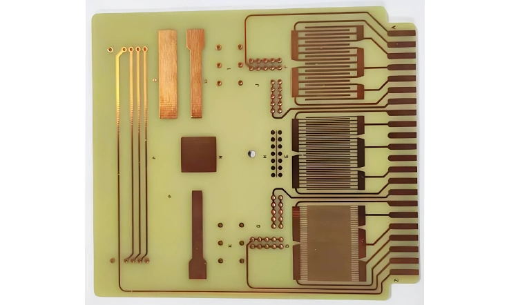
Application Showcase: RO4835 in Demanding Sectors
The true measure of a material’s success is its adoption in real-world, high-stakes applications. The deployment of RO4835 across a spectrum of high-tech industries demonstrates its versatility and its ability to deliver uncompromising performance and reliability.
●5G Telecommunications: Utilized for antenna arrays and RF front-end modules, where its low loss maintains signal integrity in sub-6 GHz and mmWave bands.
●Automotive Radar: A core material for 77/79 GHz ADAS radar systems, providing stable performance across harsh automotive temperature ranges and vibration profiles.
●Aerospace & Defense: Employed in avionics, satellite communications, and guidance systems that demand proven reliability under extreme environmental stress.
●Industrial IoT: Deployed in compact, high-density sensor and gateway modules where thermal management and signal quality are necessities in small form factors.
Design and Simulation for High-Frequency Circuits
Accurate simulation is fundamental to achieving functional designs on the first build with RO4835. This stage connects theoretical design intent with the practical conditions of PCB fabrication, enabling our engineers to evaluate and refine electrical performance prior to final layout and board fabrication.
Leveraging High-Frequency Simulation Tools
To accurately predict the behavior of electromagnetic waves on an RO4835 substrate, human rely on a suite of sophisticated software tools. Each tool offers a different lens through which to analyze the circuit, and using them in concert provides a comprehensive understanding of potential performance before fabrication.
●3D EM Simulation (e.g., HFSS): Applied for modeling passive components like antennas and filters, where visualizing electromagnetic field distribution is fundamental to performance.
●Circuit & System Co-Simulation (e.g., ADS): Facilitates the analysis of the signal path at a system level, evaluating metrics like BER and eye diagrams to ensure interoperability.
●Field Solvers (e.g., Si9000): Provide rapid and accurate extraction of transmission line parameters (impedance, loss) from a given stack-up for quick design iterations.
Creating Actionable PCB Stack-up Models
The maxim “garbage in, garbage out” is especially true for RF simulation. A simplistic model will yield inaccurate results. Creating a detailed, manufacturable stack-up model is the foundation for achieving a strong correlation between simulated predictions and real-world measurements.
Simulation Fidelity: Model Inputs vs. Simulation Output Accuracy:
| Input Parameter | Basic Stack-Up | Advanced Stack-Up (RO4835-Tuned) |
| Dielectric Constant (Dk) | Nominal only | Nominal + frequency sweep |
| Copper Roughness (Rz or SR) | Ignored | Measured, modelled (Huray model) |
| Resin Content Variation | Default (%) | Fabrication-specific |
| Simulation-Measurement Delta | >15% | <5% |
●Beyond Basic Inputs: Effective models incorporate second-order effects like copper surface roughness and resin content variations to ensure simulations closely mirror physical measurements.
●S-Parameter Analysis: The extraction of S-parameters (insertion loss, return loss, crosstalk) from the model provides a clear, quantitative basis for optimizing the layout before fabrication begins.
●Closing the Design Loop: The objective is a tight correlation between simulated and measured performance. This iterative process of modeling and refinement is the method to avoid costly redesigns.
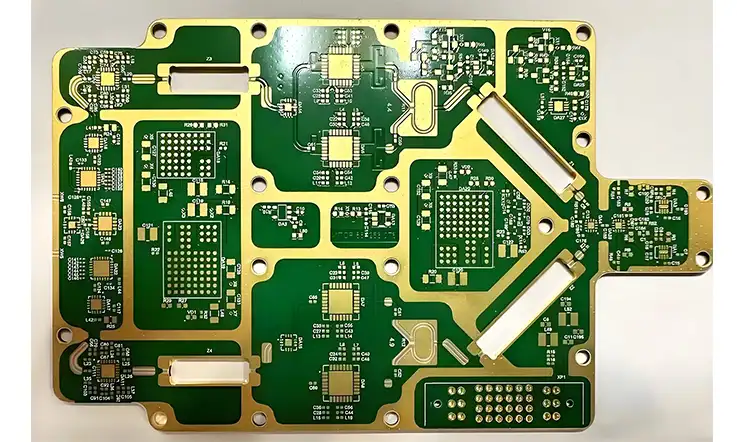
Advanced Fabrication Control for RO4835 Laminates
The superior properties of RO4835 laminates are only realized through meticulous and specialized fabrication control. The manufacturing sequence must be specifically adapted to the unique thermal and mechanical behavior of this material, ensuring that design specifications are translated into precise physical attributes on every board.
Core Process Optimization
Every fundamental step in PCB fabrication—lamination, drilling, and etching—must be fine-tuned for RO4835. Standard FR-4 parameters are insufficient and can compromise the material’s integrity. Rigorous control over these core processes guarantees performance.
●Lamination: The use of precisely defined temperature and pressure profiles achieves void-free bonding without the excessive resin flow that could alter dielectric thickness and impedance.
●Drilling: Spindle speeds, feed rates, and drill bits are selected specifically for RO4835’s composite structure to produce clean, smear-free holes for reliable plating.
●Etching & Imaging: The calibration of etching processes for different copper foil types renders sharp trace edges, which is fundamental to maintaining tight impedance control.
Mastery of Hybrid Constructions
Combining RO4835 with other materials like FR-4 in a hybrid stack-up introduces challenges due to their dissimilar properties. Success requires deep expertise in managing these differences to produce a flat, reliable, and high-performance board.
●CTE Mismatch Management: Sequential lamination and designed stack-up symmetries effectively manage the internal stresses between RO4835 and FR-4, preventing board warpage.
●Resin Flow Control: Lamination parameters are fine-tuned to accommodate the different melt-and-flow characteristics of each material, ensuring a solid and reliable bond interface.
●Collaborative DFM: The DFM process allows for finding the optimal balance between electrical requirements and manufacturability in complex hybrid builds.
Copper Foil Selection and Its High-Frequency Effects
The choice of copper foil on an RO4835 laminate is a defining engineering decision. At microwave frequencies, the foil is not a simple conductor but an active component influencing signal integrity. Understanding the interplay between copper surface roughness, the skin effect, and manufacturing processes is a prerequisite for any high-performance design.
Skin Effect and Conductor Losses
At high frequencies, current concentrates near the conductor’s surface in a phenomenon named the skin effect. The skin depth decreases as frequency increases, meaning more of the signal travels along the copper’s surface profile. This has direct consequences for signal loss.
Skin Depth vs. Frequency (Assuming Copper Conductivity at 20°C):
| Frequency (GHz) | Skin Depth (µm) | Relevance to Copper Roughness |
| 1.0 | ~2.1 | Comparable to standard ED foil |
| 10.0 | ~0.66 | Below most RTF roughness |
| 20.0 | ~0.47 | Near VLP foil Rz |
| 77.0 | ~0.24 | Skin depth ≪ rough foil |
●Surface Roughness Impact: When the copper foil’s surface roughness is comparable to the skin depth, the signal’s effective path length increases as it traverses the microscopic topography. This longer path translates directly to higher resistive losses and increased signal attenuation.
●Modeling Conductor Profile: Accurate high-frequency simulation depends on models—such as Huray or Hammerstad—that incorporate copper surface roughness. During DFM review, it’s necessary to confirm that the roughness value applied in simulation reflects the characteristics of the actual foil used in fabrication, allowing measurement outcomes to closely reflect the simulated predictions.
A Technical Comparison of Copper Foil Types
Different copper foils offer a trade-off between electrical performance, adhesion, and cost. The selection should be based on the application’s specific frequency and loss budget.
Copper Foil Comparison Table:
| Foil Type | Surface Roughness (Rz) | Insertion Loss Impact | Etch Definition | Typical Use Case |
| ED Copper | 4–6 µm | High above 6 GHz | Standard | Low-cost RF or general-purpose circuits |
| Reverse-Treated | 2.5–4 µm | Moderate | Balanced | Broadband, low-mid GHz, low-loss RF |
| VLP (Very Low Profile) | 1.5–2.0 µm | Low at mmWave bands | High precision | Automotive radar, 25G+ SerDes, 77 GHz RF |
●Standard Electrodeposited (ED) Copper: This foil has a relatively high surface roughness profile (typically Rz > 4 µm), which provides excellent adhesion. However, its roughness can noticeably increase insertion loss at frequencies above a few gigahertz. It is a cost-effective choice for less demanding applications.
●Reverse-Treated Foil (RTF): RTF is manufactured so the smoother “drum side” of the foil bonds to the dielectric. This presents a smoother path for the signal, reducing conductor losses. The etched side is treated for photoresist adhesion, offering a good balance of performance and manufacturability.
●Very Low Profile (VLP) Copper: VLP foils are engineered with extremely smooth surfaces (e.g., Rz ≈ 2 µm). They are the preferred choice for millimeter-wave applications (e.g., 77 GHz radar) and high-speed digital circuits where minimizing insertion loss is the primary objective. Their smooth surface requires more tightly controlled etching processes to achieve fine-line definition.
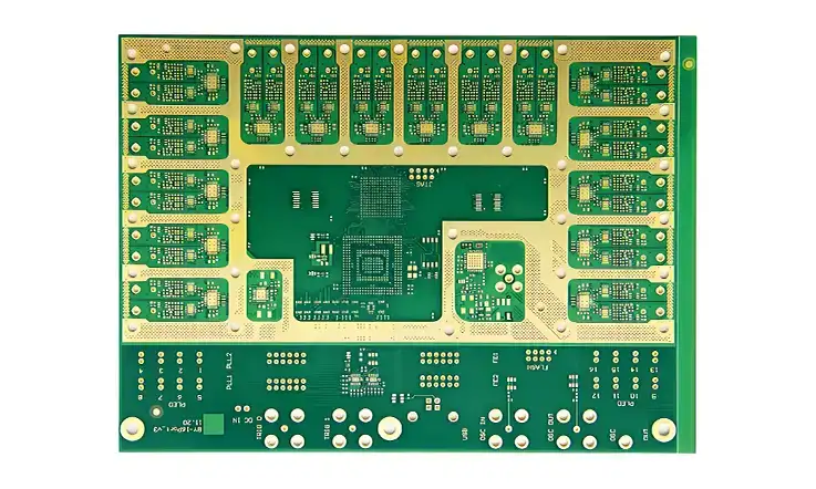
Advanced Via Structures and Their Applications
As circuit densities increase, sophisticated via structures become necessary for routing, signal integrity, and thermal management. The ability to fabricate these advanced structures on RO4835 is a hallmark of a high-capability fabrication house.
High-Density Interconnect (HDI) with Microvias
HDI technology employs laser-drilled microvias, offering substantial benefits for modern compact designs. This approach is particularly effective for RO4835 boards featuring large BGA components or dense RF modules.
●Increased Routing Density: Microvias (typically 75-150 µm diameter) require smaller pads, freeing up considerable space on surface and inner layers. This enables more complex routing in a smaller footprint without increasing the board’s layer count.
●Signal Integrity Benefits: Due to their smaller size, microvias exhibit lower parasitic capacitance and inductance than standard mechanically drilled vias. This results in better impedance control and reduced signal degradation, making them ideal for transitions near RF components.
●Sequential Build-Up (SBU) Process: HDI fabrication requires a sequential lamination process. Managing multiple lamination cycles with RO4835 and compatible dielectrics demands expertise to ensure the reliability of these complex, multi-layered structures.
Back-Drilling for High-Speed Channels
In a multilayer board, the unused portion of a via barrel, known as a stub, acts as a resonant antenna at high frequencies. This stub can cause severe signal reflections, degrading performance in high-speed digital systems.
●Stub Mitigation: Back-drilling is a controlled-depth drilling process that mechanically removes the conductive stub after primary plating. This operation requires precision Z-axis control to avoid damaging the active portion of the via.
●Performance Improvement: By removing the stub, back-drilling dramatically reduces deterministic jitter and insertion loss, improving the eye diagram opening for data channels operating at 10 Gbps and above. It is a required technique for many high-performance computing and test equipment boards.
●Design and CAM Considerations: The board layout must provide adequate clearance on adjacent layers for the back-drilling tool. CAM engineering verifies these clearances and optimizes the tool paths for a clean result.
Understanding Passive Intermodulation (PIM) in RF Designs
Passive Intermodulation (PIM) is a form of signal interference generated when two or more signals mix in a passive device that exhibits a non-linear response. In multi-carrier communication systems like 5G, PIM can elevate the noise floor and severely degrade performance.
Primary Sources of PIM on a PCB
PIM can arise from several sources on a printed circuit board, many of which are related to material selection and manufacturing quality. Identifying and controlling these sources is the method to building a low-PIM system.
●Ferromagnetic Materials: Materials like nickel, found in ENIG and ENEPIG surface finishes, are a primary source of PIM due to their non-linear magnetic properties (hysteresis).
●Contact Junctions: Any non-ideal electrical connection—such as a poor solder joint, a loose connector interface, or a micro-crack in a trace—can create a non-linear “diode effect” that mixes signals and generates PIM.
●Conductor Quality: At very high power levels, factors like rough conductor surfaces and inconsistent trace widths can contribute to non-linearity and PIM generation.
Design and Fabrication Strategies for Low PIM
Achieving low PIM performance requires a holistic approach that begins in the design phase and extends through every step of fabrication and assembly. Certain strategies are specifically aimed at PIM mitigation.
●Material and Finish Selection: For PIM-sensitive applications, designs are guided toward low-PIM finishes like Immersion Silver or OSP over bare copper. All components in the RF path (e.g., connectors) must also be specified as low-PIM.
●Process Control for Cleanliness: Fabrication processes must be designed to minimize contamination and ensure clean, well-defined conductor edges. Any metallic burrs or slivers left on the board can act as small, unintended PIM sources.
●High-Quality Assembly: High-quality soldering is needed to create robust, linear solder joints. Post-assembly inspection confirms there are no cold joints or other defects that could generate PIM.
Post-Assembly Inspection and Conformal Coating
The manufacturing sequence does not end at bare board fabrication. Post-assembly considerations are a necessity for ensuring the long-term reliability and performance of high-frequency assemblies in their operational environment.
Advanced Post-Assembly Inspection Techniques
Once components are mounted, a new set of inspection challenges arises. Advanced inspection methods can see beneath components and verify the quality of the assembly, ensuring its integrity before it goes into the field.
●Automated Optical Inspection (AOI): Used to verify component placement, orientation, and the quality of visible solder joints on assembled boards. AOI systems are calibrated to the specific requirements of RF components.
●X-Ray Inspection (AXI): A requirement for inspecting solder joints hidden underneath components like BGAs and QFNs. 2D and 3D X-ray systems allow for detection of defects like voids, shorts, and insufficient solder fill that are invisible to the naked eye.
●Assembled Board RF Testing: For specific applications, functional testing of the fully assembled board can be facilitated. This verifies that the entire signal chain, including components and solder joints, meets the required RF performance specifications.
Conformal Coating Strategies for RF Boards
Conformal coating protects PCB assemblies from moisture and contaminants, but it can also adversely affect RF performance if not managed correctly. The coating material itself acts as a new dielectric layer, altering the circuit’s electrical characteristics.
●Effect on RF Performance: Applying a coating over RF traces will change their effective Dk, leading to a shift in impedance and phase velocity. This effect is more pronounced at higher frequencies and can detune sensitive filters or antennas.
●Mitigation and Control: The effect of conformal coating must be anticipated and managed. This is accomplished by:
1.Selecting low-loss, low-Dk coating materials like acrylics or Parylene.
2.Modeling the coating’s thickness and Dk in simulation software to pre-compensate the circuit design.
3.Employing selective coating techniques, using precision masking to keep the coating off of RF-sensitive areas while still protecting the rest of the board.
The TCO Equation: A Financial Perspective on RO4835 Fabrication
Evaluating a high-performance laminate solely on its initial price is a common pitfall. The true cost of a material like RO4835 is revealed through a Total Cost of Ownership (TCO) analysis, which accounts for its impact on yield, reliability, and time-to-market.
Effect on Yield and Rework Costs
The manufacturability of a material has a direct and pronounced impact on project costs. The superior processability of RO4835 minimizes costly defects during both fabrication and assembly.
●Higher Fabrication Yields: RO4835’s robust processing characteristics lead to fewer defects like delamination or trace peel-off, reducing material scrap and rework costs.
●Lower Assembly Scrap: Its dimensional stability prevents board warp during reflow, resulting in fewer soldering defects and less need to scrap expensive, fully populated assemblies.
Reducing Project Timelines and Financial Risk
Time-to-market and long-term reliability are substantial financial metrics. The predictability and robustness of RO4835 help de-risk projects and accelerate their completion.
●Fewer Design Spins: The predictable electrical performance of RO4835 means the first physical prototype is far more likely to match the simulation, avoiding costly and time-consuming board redesigns.
●Lower Long-Term Costs: The inherent reliability of RO4835 in harsh environments reduces the probability of field failures, which carry enormous costs in terms of warranty claims, product recalls, and damage to brand reputation.
The JarnisTech Advantage: A Commitment to Excellence
The preceding sections have detailed the complex interplay between advanced materials and precision manufacturing. The successful outcome of any high-frequency PCB project hinges on the capabilities of the chosen fabrication house. JarnisTech distinguishes itself by delivering a comprehensive suite of capabilities designed to translate challenging designs into reliable, high-performance hardware.
Advanced Technological Capabilities and Process Control
A commitment to superior quality is demonstrated through investment in state-of-the-art technology and the rigorous process controls required to master it. JarnisTech’s fabrication environment is built upon this principle.
●Precision Equipment: The facility is equipped with modern machinery, including high-precision laser drilling systems for HDI microvias, vacuum lamination presses for void-free multilayer bonding, and automated optical and X-ray inspection systems for comprehensive quality verification.
●Process Mastery: Deep expertise in handling high-frequency materials like RO4835, particularly in complex hybrid stack-ups with FR-4, ensures consistent, high-yield results. This includes specialized protocols for etching, plating, and surface finishing tailored to RF applications.
●Quality Certifications: Adherence to recognized industry standards, such as ISO 9001 and IPC Class 3, provides an objective benchmark for the quality and reliability of the finished products.
Competitive Value and Transparent Lead Times
True value in PCB fabrication is a function of total cost, not just unit price. JarnisTech focuses on delivering superior value through manufacturing efficiency, transparent scheduling, and supply chain stability.
●Optimized Total Cost of Ownership (TCO): High first-pass yields and exceptional reliability minimize costly rework, assembly scrap, and field failures, delivering a lower TCO for clients on complex projects.
●Agile and Predictable Scheduling: The availability of dedicated quick-turn prototyping lines allows for rapid design iteration, while transparent communication regarding material availability and production scheduling ensures predictable delivery for volume orders.
●Supply Chain Management: Strong relationships with authorized material distributors ensure a stable supply of authentic Rogers laminates, mitigating risks associated with material shortages and counterfeit products.
Proactive Engineering Support and Client Services
Fabricating a complex RF board is a collaborative effort. JarnisTech provides a level of engineering support and service designed to function as a seamless extension of the client’s own design team.
●In-Depth DFM Analysis: Every design undergoes a thorough Design for Manufacturability review conducted by experienced RF engineers. This proactive analysis identifies and resolves potential issues before fabrication begins, saving time and resources.
●Dedicated Project Support: A dedicated contact person supports clear communication and timely updates throughout each phase—from quotation to delivery—helping maintain clarity and transparency at every step.
●Comprehensive Documentation: A full documentation package, including certificates of conformance, material traceability records, and final inspection reports, is delivered with every project, providing complete accountability and quality assurance.
Frequently Asked Questions (FAQ) about RO4835 PCB Fabrication
1.How are hybrid builds combining RO4835 and FR-4 handled?
A sequential lamination process is used with carefully developed press profiles that manage the different CTE and resin flow characteristics of each material. This expertise is fundamental for producing reliable, warp-free hybrid boards.
2.How can heat dissipation be improved on an RO4835 board?
The design should incorporate thermal via arrays directly under high-power components. The fabrication process can include filling these vias with conductive epoxy and plating them over (VIPPO), which creates a highly efficient thermal path to ground or heat-sink layers.
3.Is there a maximum layer count for RO4835?
While technically unlimited, pure RO4835 boards are most commonly seen up to 12 layers. Beyond that, cost and cumulative Z-axis tolerances become pronounced factors. Higher layer counts are achievable for specialized applications.
4.Is it possible to back-drill vias on RO4835 PCBs?
Yes. Back-drilling (controlled-depth drilling) to remove unused via stubs is an available advanced process. It measurably improves signal integrity in high-speed digital channels (≥10 Gbps) by minimizing signal reflections.
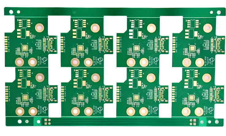
5.How does panelization strategy influence the final board cost?
Panelization directly impacts cost by affecting material usage. Efficient layouts reduce waste on high-value RO4835 panels. Balanced copper areas and symmetrical designs are also necessary to avoid warping—especially in hybrid constructions.
6.What are common but avoidable design pitfalls for RO4835?
Typical issues include:
●Ignoring copper roughness in simulations, leading to inaccurate loss values.
●Using 90° RF trace corners instead of smooth bends, causing signal reflections.
●Routing over ground splits, which disrupts return paths and increases EMI.
Our services
Rogers PCB Laminates & Series


