
A high-performance high-frequency circuit originates from a comprehensive understanding of its core material and the intricacies of fabrication. This analysis moves beyond datasheet specifications to explore the Rogers RO3203 laminate from a practical, manufacturing-focused perspective. Drawing from extensive real-world production data, this document outlines the necessary design rules, process controls, and performance insights to translate a demanding RF design into a reliable physical product.
An Analysis of Rogers RO3203 Core Material Properties
Rogers RO3203 is a high-frequency laminate engineered for applications demanding unwavering electrical performance and mechanical stability. Its composition—a ceramic-filled polytetrafluoroethylene (PTFE) composite—provides a distinct set of attributes that address the challenges of modern RF and microwave circuit manufacturing.
Electrical Characteristics as a Foundation for Performance
The predictability of a material’s electrical behavior underpins successful RF design. RO3203 exhibits a stable and reliable dielectric foundation.
●Stable Dielectric Constant (Dk): With a nominal Dk of 3.02 ± 0.04 at 10 GHz, this material offers exceptional uniformity. This tight tolerance permits designers to model impedance-controlled structures—from microstrip lines to complex differential pairs—with high confidence, minimizing the deviation between simulation and physical hardware performance.
●Low Dissipation Factor (Df): The dissipation factor, a measure of signal energy lost as heat, is approximately 0.0016 at 10 GHz. This low-loss characteristic preserves signal integrity by reducing energy depletion along high-frequency paths, resonant structures, and lengthy transmission lines.
●Panel-Wide Uniformity: In a production environment, RO3203 demonstrates remarkable dielectric uniformity from point to point across a large manufacturing panel. This isotropy helps in achieving tight tolerance margins in components like filters, couplers, and large-scale antenna arrays where phase coherence is a primary requirement.
Mechanical and Thermal Stability
Beyond its electrical merits, the mechanical robustness of RO3203 simplifies fabrication and enhances long-term reliability.
●Enhanced Rigidity: Compared to pure, unfilled PTFE laminates, the ceramic filler provides improved stiffness. This quality prevents material deformation during handling, drilling, and lamination, leading to superior dimensional control and process precision.
●High Dimensional Fidelity: The material maintains its form and dimensions with minimal deviation throughout etching, lamination, and thermal cycling. This behavior is beneficial for designs with fine features, tight-pitch BGA layouts, and complex multilayer registration, directly reducing defects related to misalignment.
●Low Moisture Absorption: RO3203 shows a very low moisture absorption rate (typically under 0.1%). This attribute prevents shifts in dielectric properties in humid environments, ensuring stable performance for devices deployed outdoors or in uncontrolled conditions, and also minimizes delamination risk during solder reflow.
●Favorable Thermal Conductivity: With a thermal conductivity of 0.79 W/m·K, the material assists in dissipating heat from active components. While not a substitute for dedicated thermal management solutions, it contributes to mitigating localized hotspots and improving overall thermal performance.
Design for Manufacturability (DFM) with RO3203
A well-simulated design can fall short of its performance goals if it overlooks the realities of physical production. Engineering a high-performance PCB with RO3203 calls for a design-for-manufacturability (DFM) approach that accounts for the material’s response to fabrication processes.
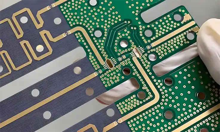
Impedance Control and Layout Strategies
Achieving precise impedance is a result of coordinating the designer’s layout with the PCB fabricator‘s process control. The stable Dk of 3.02 is a favorable starting point, but physical realization requires specific design choices.
●Etch Factor Compensation: Designers should account for etch undercut. Applying a specific etch compensation factor, determined in consultation with the fabricator, to trace widths ensures the final physical geometry matches the impedance model.
●Continuous Reference Planes: Signal layers should be referenced to a solid, uninterrupted ground or power plane. Splits or voids in the reference plane beneath a high-frequency trace will cause impedance discontinuities.
●Mitered Bends: Using mitered or arc-shaped bends for all high-frequency traces instead of sharp 90-degree corners prevents reflections and preserves signal integrity by minimizing impedance variations at the bend.
Table 1 – RO3203 PCB Impedance Planning Parameters:
| Parameter | Recommended Practice |
| Target Dielectric Constant (Dk) | 3.02 ± 0.04 (10 GHz) |
| Trace Etch Compensation | ~10% for 0.5 oz Cu, ~8% for 1 oz Cu |
| Min. Reference Plane Clearance | < 1.5x trace width (to minimize impedance swing) |
| Corner Bend Strategy | 45° mitered or arc > 3× trace width radius |
| Recommended Tolerance on Z-Height | ±10% (depends on stackup symmetry and prepreg flow) |
High-Frequency Via Design and Routing
In microwave circuits, a via is a 3D structure with inherent inductance and capacitance that can affect signal propagation if not designed correctly.
●Via Stub Mitigation: For through-hole vias in high-frequency paths (e.g., >10 GHz), via stubs can act as resonant structures. The use of back-drilling (controlled-depth drilling) removes the unused portion of the via barrel to negate this effect.
●Via Fencing for Isolation: To suppress crosstalk and isolate RF traces, via “fences” can be implemented by placing rows of ground-stitched vias parallel to the signal lines. This creates a virtual coaxial structure that contains the electromagnetic fields.
●Adherence to Aspect Ratios: The ratio of the PCB thickness to the drill diameter (aspect ratio) affects reliable copper plating. For RO3203, maintaining an aspect ratio below 10:1 facilitates optimal through-hole plating quality.
Table 2 – Via Design Guidelines for RO3203 Microwave PCBs:
| Parameter | Recommended Value / Range |
| Max Recommended Via Stub Length | ≤ 0.3 mm (for >10 GHz signals) |
| Back-Drill Depth Accuracy | ±75 μm |
| Ground Stitch Via Pitch (Fencing) | 0.75–1.0 mm (center-to-center) |
| Aspect Ratio (Thickness:Drill Dia) | ≤ 10:1 (ideal 8:1 for multilayer) |
| Plated Hole Diameter Range | 0.20 mm – 0.50 mm |
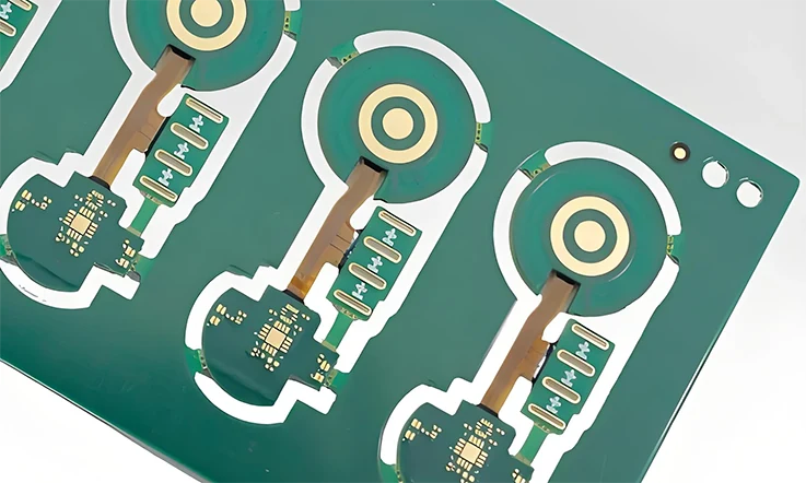
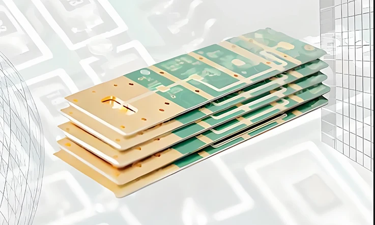
Stackup Planning for Hybrid and Multilayer Builds
The layer stackup is the architectural blueprint of the PCB. A well-planned stackup balances electrical performance, manufacturability, and cost.
●Hybrid Stackups: RO3203 is often combined with other materials. RO4450F prepreg serves as a suitable choice for bonding layers. For less demanding digital or power layers, standard FR-4 can be used to manage cost. The Coefficient of Thermal Expansion (CTE) mismatch must be managed in the lamination process.
●Symmetrical Construction: A symmetrical stackup, where layer types, thicknesses, and copper weights are mirrored around the board’s center, helps prevent warpage. This practice is particularly beneficial for larger boards or those undergoing multiple reflow cycles.
Table 3 – RO3203 Hybrid Stackup Considerations:
| Stackup Element | Typical Material Used | Notes |
| Core Dielectric Layer | Rogers RO3203 (e.g., 20mil) | Primary RF signal routing |
| Bonding Prepreg | RO4450F or RO4450B | Compatible with RO3203 and FR4 |
| Digital/Power Layers | FR-4 (170°C Tg) | Lower cost, placed away from RF layers |
| Copper Thickness | 0.5 oz – 1 oz | RF layers: 0.5 oz preferred for impedance |
| Z-Height Tolerance Management | Pressed tolerance ±10% | Use symmetrical stackup where possible |
The Precision Fabrication Process for RO3203 PCBs
Manufacturing circuit boards with RO3203 laminate requires specialized equipment and deep process knowledge. Every stage must be optimized to preserve the material’s electrical and mechanical integrity.
Material Preparation and Precision Drilling
The foundation of a high-quality RO3203 build is laid before the first hole is drilled.
●Climate-Controlled Storage and Conditioning: RO3203 laminates are stored in a humidity- and temperature-controlled environment. Before processing, panels are pre-baked using a calibrated profile to remove absorbed moisture, preventing outgassing and delamination during lamination.
●Optimized Drilling Parameters: The ceramic filler in RO3203 is abrasive. Specialized micro-grain carbide drill bits with specific flute geometries are utilized in peck-drilling cycles to produce clean, smooth hole walls free of resin smear, which facilitates reliable via plating.
●Plasma De-smear Process: After drilling, all panels undergo a plasma de-smear and etch-back process. This step removes residual PTFE resin from the inner layer copper pads within the hole, ensuring a robust electrical and mechanical connection after plating.
Multilayer Lamination and Hybrid Integration
Laminating multilayer boards, especially hybrid constructions, is a technically demanding aspect of fabrication.
●Tailored Lamination Profiles: A programmable hydraulic press with tailored temperature and pressure profiles for RO3203 and associated prepregs ensures proper resin flow and a void-free bond without exerting excessive stress on the laminate.
●Advanced Registration Systems: To counteract material movement during lamination, a combination of post-etch punching and X-ray verification is used to ensure precise layer-to-layer alignment, achieving registration tolerances tighter than the IPC Class 3 standard.
High-Frequency Surface Finishes
The surface finish on an RF board is an active component of the circuit, influencing insertion loss, solderability, and signal launch.
●Immersion Silver (ImAg): This finish is often selected for high-frequency applications. It offers low loss and a flat surface, suitable for millimeter-wave frequencies. It requires careful handling to prevent tarnishing.
●Electroless Nickel Immersion Gold (ENIG): ENIG provides a robust, solderable surface with a long shelf life, making it well-suited for mixed-signal boards. A controlled-phosphorus nickel layer is used to minimize magnetic interference.
●Finish Thickness Control: The thickness of the finish is managed closely. X-ray fluorescence (XRF) testing is used to verify that finish thicknesses are within tight specifications on every production lot.
Advanced Process Control in RO3203 Fabrication
Beyond the standard fabrication sequence, achieving superior performance and yield with RO3203 depends on the fine-tuning of advanced process controls. These methodologies differentiate standard manufacturing from high-reliability production.
Advanced Etching Techniques and Uniformity Control
Defining precise trace geometries on a PTFE-based substrate requires more than standard etching protocols.
●Spray Etching for Uniformity: In the fabrication of fine-line RF circuit boards, conveyorized spray etching systems offer greater control over line definition compared to conventional immersion methods. These systems continuously apply fresh etchant across the entire panel surface through a high-pressure spray mechanism, which helps achieve uniform etch rates and reduces dimensional variation between the panel center and outer edges..
●Etch Rate Monitoring and Compensation: The process involves real-time monitoring of the etchant chemistry and temperature. A feedback loop allows for adjustments to conveyor speed and spray pressure to maintain a stable etch rate. Artwork is compensated based on empirical data for a given copper weight and line width to precisely account for undercut, ensuring the final trace dimensions match the design model.
●Differential Etching for Surface Preparation: Before applying solder mask or a surface finish, a micro-etching step is performed. This process removes any surface oxides and creates a microroughened topography on the copper traces, which dramatically improves the adhesion of subsequent coatings.
Lamination Cycle Optimization for Hybrid Builds
The lamination of dissimilar materials in a hybrid stackup is a complex thermodynamic and mechanical challenge.
●Statistical Process Control (SPC) in Lamination: Pressure, vacuum levels, and temperature ramp rates are not just set but monitored using SPC. Any deviation outside the control limits triggers an alert. This data-driven approach ensures that every lamination cycle is repeatable and conforms to the validated profile.
●Pressure Distribution Analysis: Specialized pressure-sensitive films can be used during setup and qualification runs. These films provide a high-resolution map of the pressure distribution across the platen, identifying any potential cold or hot spots that could lead to inconsistent resin flow or delamination.
●Managing Resin Flow: When bonding RO3203 with a higher-flow prepreg like RO4450F, the lamination profile is designed with a specific “dwell” period at a temperature just below the resin’s main flow point. This allows the resin to stabilize before full pressure is applied, preventing excessive resin squeeze-out that could alter the final dielectric thickness.
Plasma Treatment Parameterization
The success of a plasma treatment step lies in the precise control of its parameters, which are tailored to the specific material and application.
●Gas Mixture Composition: A typical gas mixture for treating PTFE surfaces is a combination of an inert gas like argon (Ar) for physical bombardment, an active gas like oxygen (O2) for chemical reaction and cleaning, and often a fluorine-containing gas like carbon tetrafluoride (CF4) for controlled etching. The ratio of these gases is finely tuned to achieve the desired surface energy and topography.
●RF Power and Chamber Pressure: The RF power applied to the chamber electrodes determines the plasma density and ion energy. The chamber pressure affects the mean free path of the gas molecules. These two parameters are balanced to control the nature of the plasma, shifting it from a more chemical-etching regime to a more physical-bombardment regime depending on the goal (e.g., desmear vs. surface activation).
Performance Benchmarking: RO3203 vs. Alternative Laminates
The selection of a high-frequency laminate involves trade-offs between performance, cost, and manufacturability. Fabrication behavior often reveals differences not apparent on datasheets.
Comparison: RO3203 vs. Woven-Glass Laminates (e.g., Isola Astra MT77)
Woven-glass reinforced materials present certain manufacturing and performance characteristics.
●Weave Effect and Skew: Materials like Astra MT77 use a glass weave for reinforcement. This can cause localized Dk variations depending on the trace orientation relative to the weave, leading to timing skew in differential pairs. RO3203’s non-woven, homogenous ceramic filler avoids this “weave effect.”
●Drilling and Hole Quality: The glass fibers in woven laminates can sometimes result in fiber protrusion into the hole wall, which can affect plating adhesion. The RO3203 composite structure allows for smoother, more uniform drilled hole walls.
Table 1 – Electrical and Mechanical Comparison: RO3203 vs. Astra MT77:
| Parameter | Rogers RO3203 | Isola Astra MT77 |
| Dielectric Constant (Dk @ 10 GHz) | 3.02 ± 0.04 | 3.00 ± 0.05 |
| Dissipation Factor (Df @ 10 GHz) | 0.0016 | 0.0017 |
| Filler Type | Ceramic-filled | Woven-glass reinforced |
| Drilled Hole Wall Smoothness | High | Medium (subject to fraying) |
| Differential Pair Skew Sensitivity | Minimal | Present (due to glass weave) |
| Thickness Availability | 10mil – 60mil | 4mil – 62mil |
Comparison: RO3203 vs. Other PTFE Composites (e.g., Taconic TLY-5)
While both are PTFE-based, their filler materials lead to different manufacturing outcomes.
●Mechanical Rigidity and Handling: The ceramic filler in RO3203 provides greater mechanical stiffness compared to more flexible alternatives like TLY-5. This rigidity translates to better dimensional stability during processing.
●Plating Adhesion: The surface of RO3203, when prepared via plasma treatment, facilitates a strong copper-to-substrate bond during the electroless copper plating process, resulting in higher peel strength.
●Thermal Expansion (CTE): RO3203 exhibits a lower Z-axis (thickness) CTE compared to many other PTFE composites. This reduces stress on plated through-hole barrels during thermal cycling, improving the long-term reliability of vias.
Table 2 – Fabrication and Thermal Behavior: RO3203 vs. TLY-5:
| Parameter | Rogers RO3203 | Taconic TLY-5 |
| Base Resin | PTFE + Ceramic | PTFE + Non-ceramic Filler |
| Flexibility (Handling) | Low (Rigid) | High (Flexible) |
| Copper Peel Strength (After Plasma) | ≥ 8.5 lb/in | ~6.0–7.0 lb/in |
| Z-axis CTE (ppm/°C) | 32 | ~180–200 |
| Dimensional Stability During Etching | High | Medium |
| Typical Thicknesses Available | 10mil / 20mil / 30mil | 10mil / 20mil / 31mil |
Application-Specific Suitability of RO3203
The attributes of RO3203 make it a suitable choice for demanding RF and microwave applications.
Antenna Systems and Phased Arrays
In phased-array antennas, the phase relationship between elements is a primary design consideration.
●Phase Stability: A stable dielectric constant across the panel ensures that the electrical length of each feed line remains uniform, which is necessary for maintaining precise phase alignment in beamforming applications.
●Low Loss for High Efficiency: The low dissipation factor minimizes signal loss in the feed network, which translates to higher antenna efficiency and better system performance (G/T).
Automotive Radar and Millimeter-Wave Sensors (ADAS)
Circuits operating at 24 GHz, 77 GHz, and beyond for automotive applications demand high material performance.
●Performance at mmWave Frequencies: RO3203 maintains its low-loss characteristics and stable Dk into the millimeter-wave spectrum, making it a reliable choice for radar sensor PCBs.
●Reliability in Harsh Environments: Due to its low moisture absorption and stable thermal properties, the material maintains predictable electrical performance across varying temperature and humidity conditions.
RO3203 in Emerging High-Frequency Systems
The material’s well-controlled electrical and mechanical behavior makes it suitable for emerging communication and sensing systems. Its performance characteristics support reliable operation at higher frequencies and help address the integration demands of more advanced architectures.
5G/6G Telecommunication Infrastructure
The evolution towards higher frequency bands in telecommunications places new demands on circuit materials.
●Millimeter-Wave (mmWave) Performance: For 5G FR2 (24-52 GHz) and future 6G sub-terahertz (sub-THz) bands, the low and stable loss tangent of RO3203 helps to minimize attenuation in antenna feed networks and interconnects, which is a limiting factor at these frequencies.
●Massive MIMO and Beamforming: The uniform dielectric constant of RO3203 benefits the performance of Massive MIMO antenna arrays, where precise phase velocity must be maintained across hundreds of radiating elements to enable accurate beam steering. The material’s tightly controlled electrical properties support this requirement by minimizing variation in signal propagation across the array.
●Thermal Management in Active Antennas: Modern active antenna systems integrate power amplifiers directly with the antenna elements. The thermal conductivity of RO3203, while moderate, aids in spreading heat away from these active components, helping to maintain stable device performance.
Aerospace and Satellite Communications (SATCOM)
In aerospace and satellite applications, reliability and stability under extreme conditions are primary requirements.
●Low Outgassing Properties: In the vacuum of space, materials that release trapped gases (outgassing) can contaminate sensitive optical systems or electronics. RO3203 exhibits low Total Mass Loss (TML) and Collected Volatile Condensable Materials (CVCM), making it suitable for space-borne applications.
●Thermal Cycling Resilience: Satellites in low Earth orbit experience extreme temperature swings. The low Z-axis CTE of RO3203 and its mechanical stability reduce the risk of via failures and material fatigue over thousands of thermal cycles.
●Radiation Tolerance: While no organic material is immune to radiation, the stable chemical structure of the PTFE matrix in RO3203 provides a degree of resilience to the types of radiation encountered in some space environments, showing less degradation in its electrical properties compared to many standard epoxy-based substrates.
Quality Assurance and Reliability in RO3203 Fabrication
Delivering a high-performance RO3203 PCB depends on a commitment to quality control at every stage.
In-Process Inspection and Electrical Testing
A suite of inspection and testing protocols is used to ensure every board aligns with its design intent.
●Automated Optical Inspection (AOI): After etching, every layer is scanned by AOI systems to detect defects in trace width, spacing, or feature formation.
●Time-Domain Reflectometry (TDR) Testing: For all impedance-controlled designs, a TDR coupon is fabricated and tested on every production panel. This provides empirical, measured data of the final impedance values.
●X-Ray Verification: For multilayer boards, X-ray inspection after lamination is used to verify layer-to-layer registration and check for internal defects before drilling.
Thermal Stress Testing and Compliance
Boards can be built to endure challenging operational conditions.
●Solder Float and Thermal Stress Testing: Sample boards from production lots can be subjected to thermal stress tests to verify the integrity of the lamination and the plated through-holes.
●RoHS and REACH Compliance: Full material traceability allows for the fabrication of RO3203 PCBs that are compliant with RoHS and REACH directives.
●Cross-Section Analysis: Micro-section analysis (cross-sections) can be performed to provide a microscopic view of hole wall quality, plating thickness, and layer registration.
Environmental and Mechanical Reliability Testing
For applications in aerospace, automotive, and other high-consequence fields, standard quality assurance is just the baseline. Advanced reliability testing is performed to qualify a design and manufacturing process, ensuring survivability in the intended service environment.
Thermal Shock and Cycling Analysis
This testing evaluates the PCB’s ability to withstand rapid and repeated temperature changes, simulating years of operational life in a compressed timeframe.
●Test Methodologies: Boards are subjected to testing in computer-controlled thermal chambers according to standards like JESD22-A104 or MIL-STD-883. A typical profile involves rapid transitions between extreme cold (e.g., -40 degrees C) and extreme hot (e.g., +125 degrees C), with dwell times at each temperature to allow for thermal stabilization. The test may run for hundreds or even thousands of cycles.
●Failure Detection: After cycling, boards are rigorously inspected for failure modes. This includes daisy-chain resistance monitoring during the test to detect intermittent opens. Post-test analysis involves cross-sectioning vias to look for micro-cracks in the copper plating, delamination at material interfaces, or solder joint fatigue. RO3203’s low Z-axis CTE gives it a distinct advantage in passing these demanding tests.
Vibration and Mechanical Shock Qualification
These tests ensure the PCB assembly can survive the physical stresses of launch, transportation, or operational movement without mechanical or electrical failure.
●Sinusoidal and Random Vibration: The PCB assembly is mounted on a shaker table and subjected to a defined vibration profile, often specified by standards like MIL-STD-810G. Sinusoidal sweeps identify resonant frequencies of the board and its components, while random vibration simulates a more realistic, multi-frequency operational environment.
●Mechanical Shock Testing: This test simulates sudden impacts or drops. The board is subjected to high acceleration (high G-force) pulses of a specific shape (e.g., half-sine) and duration.
●Data Analysis: During testing, accelerometers on the board monitor its response. Post-test inspection looks for cracked solder joints, component dislodging, or damage to the board structure. The inherent stiffness of the RO3203 laminate, compared to unfilled PTFE, contributes to better performance under these conditions by reducing board flexure.
Conductive Anodic Filament (CAF) Resistance Evaluation
CAF is a failure mode involving electrochemical migration of copper along the substrate’s fiber-resin interface, leading to short circuits. It is a concern in high-humidity, high-voltage-bias environments.
●Test Procedure: A specific test pattern with closely spaced, oppositely biased vias is fabricated. These test coupons are then placed in a high-temperature, high-humidity chamber (e.g., 85 degrees C / 85% RH) with a continuous voltage bias applied for an extended period (e.g., 1000 hours). The leakage current between the biased conductors is continuously monitored.
●Material Performance: The resistance to CAF formation is highly dependent on the quality of the resin system and its bond to the internal reinforcement. RO3203’s homogenous, ceramic-filled structure and very low moisture absorption provide an inherently high resistance to this failure mechanism, as there are no glass-fiber pathways for the migration to occur. This offers a reliability advantage over some woven-glass materials in humid operating conditions.
Failure Analysis and Prevention in RO3203 Fabrication
Expertise in high-frequency PCB manufacturing includes an understanding of potential failure modes and how to prevent them. For a material like RO3203, mitigating these challenges leads to higher yields and reliability.
Failure Mode 1: Pad Lifting and Delamination
The interface between the copper foil and the PTFE substrate can be a point of failure if not managed correctly.
●Root Causes: This issue can stem from thermal shock during assembly, insufficient surface preparation, or CTE mismatch stress.
Prevention Strategies:
1.Optimized Plasma Treatment: A properly executed plasma treatment cycle chemically alters the PTFE molecular structure, creating an active, textured surface for a superior covalent bond with the plated copper.
2.Use of Reverse-Treated Copper Foil: Reverse-treated copper foils have a specialized micro-roughened matte side that increases the surface area for bonding, creating a stronger mechanical anchor to the substrate.
3.Controlled Thermal Profiles: The use of carefully ramped temperature profiles during fabrication and assembly minimizes induced stress.
Failure Mode 2: Plated Through-Hole (PTH) Barrel Cracking
A crack in a PTH barrel can lead to an open circuit, often difficult to diagnose in a finished assembly.
●Root Causes: The high Z-axis CTE of PTFE materials is a primary driver. As the board heats, the substrate expands more in its thickness than the copper barrel, putting stress on the plating. Poor drilling quality or insufficient copper plating thickness exacerbates this.
Prevention Strategies:
1.Drill-Smear Removal via Plasma Etch-Back: A plasma de-smear process with a controlled “etch-back” step removes smear and micro-etches the substrate around the inner-layer interconnects, creating a “three-point anchor” for the subsequent plating.
2.High-Throwing-Power Plating Chemistry: Advanced, high-throw-power copper plating baths are designed to deposit copper evenly throughout the entire length of a hole, even in high-aspect-ratio designs. Cross-section analysis verifies uniform plating.
3.Stringent Thermal Stress Testing: Coupons from multilayer lots can be subjected to multiple cycles of thermal shock testing, followed by cross-section analysis to proactively search for any signs of micro-cracking.
Case Study: Fabricating a 77 GHz Automotive Radar Sensor on RO3203
A real-world example illustrates the synthesis of material science and process control. This case study outlines the approach to a 77 GHz automotive radar module.
The Challenge: Demanding Performance and Reliability Requirements
A Tier-1 automotive supplier required a next-generation radar sensor design with a demanding set of specifications.
●Electrical Requirements: The design featured a large patch antenna array requiring phase matching to within ± 2 degrees. Insertion loss on primary signal feeds had to be below 0.8 dB at 77 GHz. Impedance for the microstrip lines was specified at 50 Ohm ± 2%.
●Mechanical and Thermal Requirements: The board was an 8-layer hybrid stackup, combining RO3203 and FR-4 cores. It had to pass automotive-grade thermal cycling from -40 degrees C to +125 degrees C without any degradation in performance.
●Manufacturability Constraints: The layout included a fine-pitch (0.4mm) BGA, blind microvias, and back-drilling on high-speed digital lines.
Table 1 – Project Specification Summary:
| Parameter | Specification |
| Radar Frequency Target | 77 GHz |
| Stackup Type | 8-layer hybrid (RO3203 + FR-4) |
| Microstrip Impedance | 50 Ω ± 2% |
| Insertion Loss Spec (Primary Path) | ≤ 0.8 dB @ 77 GHz |
| Operating Temperature Range | -40 °C to +125 °C |
| BGA Pitch | 0.4 mm |
| Microvia Layers | L1–L2, L2–L3 (blind) |
| Surface Finishes | Immersion Silver (RF), ENEPIG (BGA) |
The Solution: A DFM and Process-Driven Approach
The engagement began with a collaborative review to ensure the design was optimized for successful manufacturing.
Collaborative Design for Manufacturability (DFM):
●A full DFM analysis identified that the initial stackup could lead to reliability issues. A revised stackup was proposed, strategically placing RO4450F prepreg to buffer stress from CTE mismatch.
●Field solver simulations were used to recommend a minor 4µm adjustment to RF trace widths to account for the specific etch factor, centering the final impedance at 50 Ohm.
●Specific design rules for via-in-pad structures and back-drilling clearance were provided.
Precision Fabrication Execution:
●Lamination: The hybrid stackup was laminated using a multi-step, sequential press cycle with controlled temperature ramps.
●Imaging and Etching: Laser Direct Imaging (LDI) achieved the required resolution for fine features. A controlled spray-etching process ensured uniform trace definition.
●Finishing: Immersion Silver (ImAg) was selected for the RF layers to minimize loss at 77 GHz, while the BGA pads received an ENEPIG (Electroless Nickel Electroless Palladium Immersion Gold) finish.
The Result: Achieving Performance and Reliability Targets
The combination of proactive DFM and meticulous process control produced a product that met the client’s objectives.
●Verified Electrical Performance: Post-production TDR testing on impedance coupons from every panel showed an average impedance of 49.9 Ohm with a deviation under ± 1.5%. Network analyzer measurements confirmed insertion loss and phase matching specifications were met.
●Proven Reliability: A sample set of boards passed 1000 cycles of automotive-grade thermal testing without a single failure. Cross-section analysis confirmed excellent via integrity.
●Successful Project Delivery: The production run was completed on schedule, allowing the client to meet its product launch timeline.
Table 2 – Post-Fabrication Testing Summary:
| Test or Metric | Result / Observation |
| TDR Impedance (avg) | 49.9 Ω ±1.5% deviation |
| Insertion Loss at 77 GHz | 0.74 dB (measured) |
| Phase Deviation (Antenna Array) | ±1.7° max |
| Thermal Cycling (1000 cycles) | Passed – no failure |
| Cross-Section Analysis | Strong via walls, good plating adhesion |
| Yield Rate (Prototype Batch) | >97% first-pass yield |
Technical Resources and Stackup Examples
Practical stackup examples and technical data can help bridge the gap between design theory and production reality.
Common Stackup Variants
These examples represent common, manufacturable stackups.
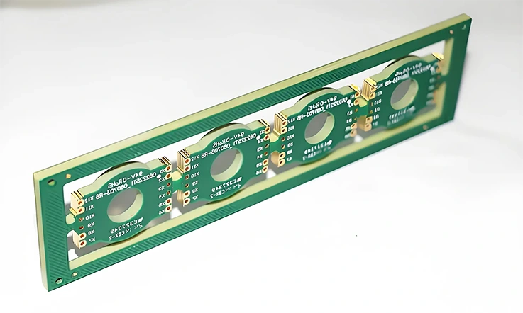
2-Layer RF Board (e.g., for Antennas/Couplers):
●Layer 1: 1 oz (35µm) Copper
●Dielectric: 20 mil (0.508mm) Rogers RO3203 Core
●Layer 2: 1 oz (35µm) Copper
4-Layer Hybrid RF/Digital Board:
●Layer 1: 1 oz Copper (RF Signals)
●Dielectric 1: 10 mil (0.254mm) Rogers RO3203 Core
●Layer 2: 1 oz Copper (Ground Plane)
●Bonding Prepreg: Rogers RO4450F
●Layer 3: 1 oz Copper (Power Plane)
●Dielectric 2: 30 mil (0.762mm) FR-4 Core
●Layer 4: 1 oz Copper (Digital Signals)
Frequently Asked Questions (FAQs):
1. Is component rework possible on an RO3203 PCB?
Rework is possible but requires precise thermal control. The substrate is more sensitive to localized heat than FR-4. Use of a pre-heater and a temperature-controlled soldering station is recommended to prevent pad damage.
2. Can RO3203 PCBs be panelized using V-scoring?
Tab-routing with perforations is strongly recommended. V-scoring can introduce micro-fractures into the ceramic-filled composite, potentially affecting the board’s integrity along the edges.
3. What solder mask is recommended for RO3203?
A high-adhesion Liquid Photoimageable (LPI) solder mask is standard. A plasma treatment cycle before mask application promotes strong, long-term adhesion to the PTFE-rich surface.
4. Does machining RO3203 accelerate tool wear?
Yes. The ceramic filler is abrasive and causes faster wear on drill and router bits compared to FR-4. Specialized carbide tools are required for volume production.
5. What is the typical lead time for RO3203 laminate?
The lead time for this specialty material is considerably longer than for FR-4, and can range from several weeks to months from distributors, depending on the specific thickness and supply chain demand.


