
In modern electronics, a landscape defined by the accelerating speed and complexity of 6G systems, artificial intelligence, and autonomous machinery, the physical medium for signal transmission graduates from a mere conduit to the ultimate arbiter of system viability. As data transfer rates escalate into the demanding strata of 112 Gbps and 224 Gbps PAM4, conventional printed circuit board materials begin to fail, their inherent physical limitations forming an unyielding barrier to progress. The selection of a laminate system, therefore, is not a simple choice but a foundational decision, one that dictates the performance ceiling of an entire technological endeavor. MEGTRON-2, a material conceived for these formidable frontiers, is acknowledged for its exceptionally low signal loss and profound reliability.
This guide provides a comprehensive exploration of the end-to-end sequence of operations, from predictive design analysis and advanced computational simulation to the exacting methodologies of fabrication and the unyielding protocols of quality verification for MEGTRON-2 based circuit boards. The singular aim is the masterful translation of this substrate’s latent potential into a tangible, field-proven circuit board—an artifact of engineering that performs with unwavering fidelity to its design.
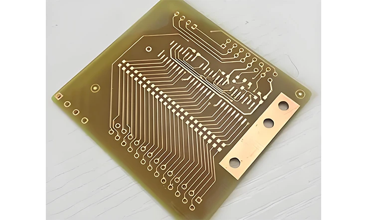
The High-Speed Design Imperative: An Examination of FR-4’s Obsolescence
The function of a high-performance PCB circuit board solution is to secure the operational success of the final product. For modern high-speed designs, the utilization of traditional FR-4 substrates does not represent a viable path to achieving performance targets. An understanding of these limitations guides the selection of advanced materials.
●Signal Energy Dissipation: The inherent nature of FR-4 causes it to absorb and dissipate high-frequency signal energy, a flaw that complicates design and generates unwanted thermal loads.
●Dielectric Inconstancy: The shifting electrical properties of FR-4 with frequency make the precise, stable impedance required by modern interfaces an unattainable goal.
●Thermal Fragility: The material lacks the constitution to reliably endure the thermal rigors of contemporary lead-free assembly, posing a risk of structural failure.
●Hygroscopic Weakness: A propensity to absorb moisture creates a latent threat of catastrophic failure during the high temperatures of the soldering process.
These combined weaknesses form a stark performance boundary, a wall against which ambitions for higher data rates and denser designs must break. To build beyond this wall requires a substrate forged from a different philosophy, with intrinsically superior physical character.
The Business Case: An Analysis of the Total Cost of Ownership for Advanced PCBs
For project managers and chief technical officers, the decision to engage a high-expertise fabrication service for a MEGTRON-2 board is a strategic financial calculation. While the initial quotation may appear higher than for standard fabrication, a clear-eyed analysis of the Total Cost of Ownership (TCO) reveals a powerful economic argument. The conversation shifts from initial expense to long-term value and risk mitigation.
The quantifiable cost of avoiding just one re-spin—a cost that includes new tooling, scrapped materials, and hundreds of precious engineering man-hours—often eclipses the entire cost differential for engaging a high-expertise fabrication service.
How First-Pass Success Mitigates Development Costs and Delays?
The most insidious cost in hardware development is time lost. A single circuit board re-spin, forced by unforeseen signal integrity failures or manufacturability problems, can derail a product launch by weeks or months, forfeiting revenue and market initiative.
●Maximizing the Probability of Success: The synergy between a stable, predictable material like MEGTRON-2 and a rigorous, simulation-driven design-for-manufacturing (DFM) process dramatically elevates the probability of first-pass success.
●Accelerating Time-to-Validation: When a physical board performs in lockstep with its simulation, the engineering team can move through the validation phase with speed and confidence. The lengthy, frustrating cycles of debugging and troubleshooting are drastically compressed, accelerating the entire journey to market.
Example: Impact of First-Pass Success on Development Timeline and Cost
| Metric | Standard PCB Fabrication | MEGTRON-2 Fabrication with High-Expertise Service |
| Average Number of Re-Spins | 2 | 0.5 |
| Average Delay per Re-Spin (weeks) | 6 | 1.5 |
| Engineering Hours Lost | 300 | 75 |
| Additional Costs per Re-Spin ($) | 50,000 | 12,500 |
| Total Estimated Delay (weeks) | 12 | 0.75 |
The Long-Term Value of Field Reliability and Brand Reputation
The financial fallout from a product failure in a deployed system can be immense, a cascade of warranty claims, replacement logistics, and the intangible yet profound erosion of brand reputation.
●Enhancing Deployed Product Lifespan: The superior thermal stability and robust mechanical nature of a meticulously fabricated MEGTRON-2 board directly translate to a more durable and reliable end product. These boards are inherently less susceptible to insidious, time-based failure mechanisms like thermal stress cracking or CAF (Conductive Anodic Filament) formation over their specified operational lifetime.
●Safeguarding a Reputation for Excellence: In the demanding arenas of aerospace, medical technology, and enterprise hardware, reliability is not just a feature; it is the currency of trust. A field failure is a breach of that trust. Investing in a robustly fabricated board is a direct investment in a product’s—and a company’s—reputation for unwavering quality.
Example: Comparison of Failure Rates Over Product Lifecycle
| Failure Mode | Standard PCB (%) | MEGTRON-2 PCB (%) |
| Thermal Stress Cracking | 5.2 | 1.1 |
| Conductive Anodic Filament | 3.5 | 0.6 |
| Total Field Failure Rate | 8.7 | 1.7 |
| Average Warranty Cost ($) | 120,000 | 25,000 |
Gaining a Competitive Edge with Built-in Performance Headroom
Fabricating a board on a high-performance material platform endows it with inherent performance margins—a well of potential that can be drawn upon for future commercial advantage.
●Extending Product Lifecycle Value: A board with ample performance headroom can often support future firmware upgrades that unlock higher data rates or more sophisticated features. This capability can breathe new life into a product line, extending its revenue-generating window and maximizing the return on the initial NRE (Non-Recurring Engineering) investment.
●Forging a Market Leadership Position: Delivering a product whose performance is demonstrably superior and more stable than its competitors is a powerful market differentiator. It justifies a premium position and builds a moat against competitors constrained by lesser materials and processes.
Example: Performance Margin Impact on Product Lifecycle and Revenue
| Metric | Conventional PCB | MEGTRON-2 PCB |
| Supported Max Data Rate (Gbps) | 56 | 112+ |
| Firmware Upgrade Potential | Limited | Extensive |
| Expected Product Lifecycle (years) | 3 | 6 |
| Estimated Incremental Revenue ($ millions) | 0 | 15 |
The Art of MEGTRON-2: How a Premier Substrate is Mastered?
Now that the practical advantages of advanced materials have been clearly outlined, the next step is to examine the precise engineering required to fully utilize their capabilities. Working with MEGTRON-2 involves more than selecting a high-performance laminate—it requires a deep understanding of its distinct processing behavior. Consistently achieving its performance potential depends on careful control across every fabrication stage. The following sections explain how its unique characteristics are translated into measurable performance benefits through disciplined process management.
Translating Material Properties into Verifiable Board-Level Performance
Engineering and fabrication disciplines converge on a single goal: to alchemize the distinct attributes of MEGTRON-2 into specified, verifiable results.
●Enabling Higher Signal Velocities: Through the meticulous architecture of the PCB stackup, the low dielectric constant (Dk) of MEGTRON-2 is leveraged to create a faster medium for signal propagation. This directly shortens transmission delays, providing the precious picoseconds needed to meet demanding timing budgets.
●Preserving the Faintest of Signals: The material’s exceptionally low dissipation factor (Df) is consciously exploited to create pathways where high-frequency signals can travel with minimal energy loss. Their amplitude and clarity are preserved over longer distances, safeguarding the integrity of the data they carry.
●Forging Reliability for Assembly and Beyond: The high glass transition temperature (Tg) of MEGTRON-2 endows a board with the fortitude to endure the thermal ordeal of lead-free soldering, not once, but multiple times. This ensures the board’s physical integrity remains uncompromised, ready for a long operational life.
●Sculpting Impedance with Precision: The confluence of disciplined process control and the material’s innate uniformity allows for the fabrication of circuit boards with tightly governed characteristic impedance, held within a ±5% tolerance. This precision forges a physical reality that performs in lockstep with its digital simulation.
Sample Data Table: MEGTRON-2 Material Properties and Board-Level Performance
| Property | Value | Notes |
| Dielectric Constant (Dk) | ~3.0 | Supports high signal velocity |
| Dissipation Factor (Df) | ~0.004 | Low energy loss for high-frequency signals |
| Glass Transition Temp (Tg) | > 200°C | Supports multiple lead-free solder cycles |
| Impedance Tolerance | ±5% | Controlled through precise fabrication |
| Signal Propagation Delay | Reduced by ~10-15% | Compared to standard FR4 |
The R-1577 & R-1570 System: A Foundation of Dielectric Stability
A steadfast and reliable multilayer circuit board begins with the artful handling of its constituent dielectric materials. The fabrication sequence is a choreographed effort to maximize the symbiotic properties of the MEGTRON-2 core and prepreg system.
●Building upon a Dielectric Foundation: The R-1577 core material is employed as the serene dielectric foundation for layers bearing the most sensitive signal traces, establishing an environment of electrical predictability.
●The Art of a Void-Free Lamination:The lamination process involves precisely controlled heat and pressure, tailored to match the specific flow characteristics of the R-1570 prepreg. This controlled environment ensures the resin distributes uniformly, filling even the finest surface features of the copper layer. Complete resin coverage eliminates voids, which is a core requirement for maintaining consistent impedance throughout the multilayer structure.
●Achieving a Homogeneous Dielectric Soul: Through controlled integration, these materials enable a circuit board structure in which the dielectric properties are maintained uniformly along the vertical build-up. This carefully engineered uniformity supports the reliable fabrication of multilayer designs with high layer counts and repeatable process outcomes.
Sample Data Table: R-1577 Core and R-1570 Prepreg Characteristics
| Material Parameter | R-1577 Core | R-1570 Prepreg |
| Dielectric Constant (Dk) | ~3.0 | ~3.0 |
| Dissipation Factor (Df) | ~0.004 | ~0.004 |
| Tg (Glass Transition Temp) | > 200°C | > 200°C |
| Resin Flow (viscosity) | N/A | Controlled for void-free lamination |
| Void Rate | <0.1% | Achieved via precise lamination |
| Thickness Tolerance | ±5% | ±5% |
MEGTRON-2 as a Balanced High-Speed PCB Material Platform
An effective engineering consultation begins with a thorough evaluation of candidate materials—not to seek a universal solution, but to match material attributes to project-specific requirements across signal speed, thermal behavior, and manufacturability. MEGTRON-2 occupies a favorable position in this spectrum. It delivers a balanced performance profile—combining a low dissipation factor (~0.004), a glass transition temperature above 200°C, and a track record in complex, high-layer digital systems. This enables stable fabrication of monolithic, high-density circuit boards designed for AI computing, defense-grade platforms, and 112+ Gbps data applications.
1.Rogers 4000 Series – Precision for High-Frequency Environments
The Rogers 4000 series represents a specialized material family tuned for RF and microwave applications. Known for temperature-stable Dk values and a high Tg exceeding 280°C, these materials are well suited to filters, amplifiers, and other analog RF modules. Their dissipation factor (~0.0037) supports sharp signal integrity at high frequencies, but hybrid constructions often required for cost or layout reasons can pose integration challenges—particularly at material boundaries. Despite exceptional electrical performance, their use is best reserved for designs where RF predictability outweighs mixed-signal complexity.
2.Taconic TLY Series – Ultra-Low Df for Millimeter-Wave Systems
Taconic TLY laminates offer an extremely low dissipation factor approaching 0.0009, making them a strong candidate for ultra-high-frequency applications such as 77GHz automotive radar and satellite downlinks. However, these benefits are paired with the complexity of PTFE-based processing, which demands special attention during fabrication. The relatively lower Tg (~180°C) compared to other high-speed laminates also narrows their application window. These trade-offs make TLY ideal for narrowband use cases at mmWave frequencies, rather than broad-spectrum digital infrastructure.
Sample Data Table: Comparison of High-Speed Laminate Materials
| Property | MEGTRON-2 | Rogers 4000 Series | Taconic TLY Series |
| Dielectric Constant (Dk) | ~3.0 | ~3.38 | ~2.17 |
| Dissipation Factor (Df) | ~0.004 | ~0.0037 | ~0.0009 |
| Glass Transition Temperature (Tg) | > 200°C | > 280°C | ~180°C |
| Suitability | Digital, High-layer | RF, Microwave | Millimeter-wave, Narrowband |
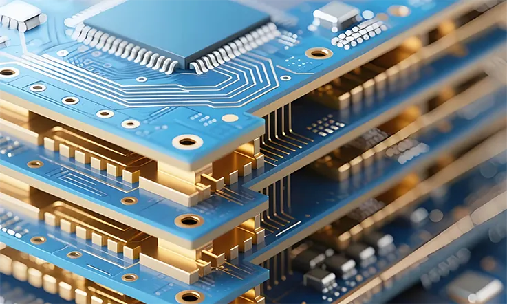
From Your Design to Finished Board: The End-to-End Fabrication Sequence
Having established the material’s character, the focus now shifts to the meticulous process that transforms these properties into a physical, high-performance artifact. The value delivered is the tangible result of a meticulously orchestrated sequence that translates a digital design into a fully functional physical reality.
Stage 1: Predictive Design Analysis and Simulation for Layout Validation
Before physical creation, there is computational validation. This front-end engineering process uses a suite of advanced simulation tools to confirm a design’s manufacturability and performance potential on the MEGTRON-2 material platform.
●AI-Assisted Stackup Architecture: A design’s constraints and performance targets serve as inputs for AI-assisted modeling software. This software explores a vast design space of stackup permutations, proposing a structure that finds an elegant equilibrium between impedance control, signal integrity, and thermal management, all while respecting the boundaries of high-yield manufacturability.
●Validation of High-Speed Channels: 3D electromagnetic field solvers are marshaled to create a high-fidelity digital twin of the most demanding signal channels. This simulation yields a rich dataset of predictive performance metrics, including insertion loss (SDD21) and return loss (SDD11). The findings from this digital exploration inform concrete recommendations for layout improvements, such as the strategic use of back-drilling.
●Holistic EMI/EMC Layout Review: The layout is subjected to a deep analysis to verify the soundness of its EMI/EMC control strategy. This review scrutinizes the continuity of reference planes, the intelligent placement of via stitching fences, and the low-impedance design of the power distribution network (PDN), all to preemptively quell the specter of electromagnetic interference.
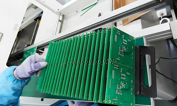
Stage 2: Precision Fabrication Methodologies for Advanced Substrates
The fabrication setting operates with exacting control, with each process carefully adjusted to accommodate the distinct processing behavior of advanced laminate materials.
●Realization of High-Density Interconnects: Finely controlled CO2 and UV laser systems sculpt microvias and form Via-in-Pad (VIP) structures, fulfilling the demands of high-density interconnect (HDI) designs. These microscopic features are the conduits that enable dense component populations and shorter, purer signal journeys.
●Execution of High-Pressure Lamination Cycles: Within the chambers of vacuum-assisted lamination presses, computer-guided profiles of heat and immense pressure are applied. These bespoke cycles, tailored for MEGTRON-2, coax the laminate stack into a single, monolithic structure, perfectly bonded and free of internal stress.
●Application of Back-Drilling for Signal Purity: For the highest-speed channels, a controlled-depth back-drilling operation excises the non-functional stub of a via barrel—a tiny, disruptive antenna that can create signal-corrupting reflections. Its removal is a testament to an unwavering commitment to signal purity.
●Plasma-Based Hole Wall Preparation: After drilling, the nascent via walls are bathed in an energized plasma of specific gases (like CF4/O2). This plasma de-smear process violently yet precisely ablates any resin residue, unveiling a microscopically textured surface, hungry for the strong, permanent adhesion of electrolytic copper.
Stage 3: Copper Interface Optimization via Strategic Surface Finishes
The fabrication process concludes with the application of the surface finish—an essential interface where the completed circuit interacts with its external environment. Selecting and applying this layer involves precise engineering decisions based on functional performance and long-term reliability
1.Conductor Surface Topography Control:
The entire fabrication sequence is geared toward producing the smoothest possible copper surfaces. This begins with the selection of very-low-profile (VLP) copper foils and is maintained through etching processes that are chemically balanced to minimize surface roughening. This relentless focus on smoothness directly combats the signal-degrading skin effect at high frequencies.
2.Application-Specific Finish Selection:
The circuit board receives a surface finish selected to suit its intended application. For designs emphasizing signal integrity and conductivity, Immersion Silver (ImAg) is often applied. In cases where enhanced soldering performance is required—particularly for fine-pitch BGA components—ENEPIG (Electroless Nickel Electroless Palladium Immersion Gold) offers a layered metallurgical structure that provides reliable wetting, oxidation resistance, and durability during assembly.
Stage 4: High-Tg SMT Assembly and Turnkey Board Realization
Following fabrication, the bare board proceeds directly to surface mount technology (SMT) assembly, where precision equipment and process control integrate components onto the substrate, completing the functional build.
●Mastery of High-Tg Reflow Soldering: Assembling a MEGTRON-2 board with high thermal mass requires precise thermal profiling. Carefully calibrated multi-zone reflow processes are applied—raising the board temperature in controlled increments to achieve optimal solder reflow, followed by a gradual cooldown to minimize thermal stress.
●Assembly of Complex, High-Density Boards: The SMT lines are state-of-the-art, capable of placing components as small as the 01005 package or as complex as large-scale FPGAs and RF modules. After placement, automated inspection systems—optical and X-ray—verify the work, ensuring every one of thousands of solder joints is flawless.
Case Study: The Anatomy of a 32-Layer SATCOM Signal Processing Solution
To give form to these abstract capabilities, consider the anatomy of a recent solution: the fabrication of a 32-layer signal processing board for a next-generation satellite communications payload. This was a board destined for the unforgiving environment of space, bearing multiple high-power FPGAs and thousands of components, all interconnected by a web of 112 Gbps channels.
The Engineering Challenges Presented:
1.An Unforgiving Signal Integrity Budget: The 112 Gbps PAM4 channels demanded a verified insertion loss below -15 dB at the 28 GHz Nyquist frequency, a target leaving no room for error.
2.A Severe Thermal Environment: The FPGAs, each a furnace dissipating over 150W, had to be cooled in the vacuum of space, demanding that the PCB itself become an active part of the thermal solution.
3.An Unwavering Reliability Mandate: The board was required to function flawlessly for a 15-year mission, enduring thousands of extreme thermal cycles from sun exposure to shadow.
4.A Formidable Fabrication Task: The sheer physical nature of the 32-layer, 4.1mm thick stackup presented profound challenges to drilling, plating, and achieving lamination uniformity.
The Executed Engineering and Manufacturing Solution:
●Collaborative Design and Architectural Refinement: The engagement began with a deep, collaborative review, culminating in a finalized 32-layer MEGTRON-2 stackup. The subsequent high-fidelity simulations were not merely a check; they were a revelation, proving that meeting the loss budget would necessitate the back-drilling of over 2,000 vias. To solve the thermal puzzle, a bespoke embedded copper coin solution was architected and integrated into the stackup, creating a high-conductivity thermal superhighway.
●A Symphony of Precision Fabrication: The board’s fabrication involved four consecutive lamination cycles, each followed by thorough inspection of the sub-assembly before moving forward. Plasma de-smear and precise back-drilling processes were performed with exacting control. The quality of these internal steps was verified through micro-sectioning analysis on test coupons from the same panel, offering clear evidence of the internal structure’s soundness.
●Advanced Assembly and Unflinching Verification: A custom, gradual-ramp reflow profile was executed. Following assembly, 100% 3D X-ray inspection peered deep inside every BGA to hunt for any microscopic voids or shorts. The final, assembled board was then subjected to a grueling battery of tests, including TDR impedance verification and VNA S-parameter measurements.
The triumphant result was a near-perfect correlation between the final, physical measurements and the initial digital simulations.
Key Project Outcomes:
●Met a stringent -15 dB insertion loss budget at 28 GHz.
●Successfully managed a >150W thermal load per FPGA via an integrated copper coin.
●Achieved first-pass success on a complex 32-layer board, securing a non-negotiable launch window.
●Delivered fully compliant, flight-ready hardware that transformed a high-risk project into a validated success story.
The Zero-Defect Framework: A Philosophy of Uncompromising Quality Verification
For applications where the cost of failure is immeasurable, the entire fabrication operation is underpinned by a philosophy of uncompromising quality control and verification.
Exceeding Industry Standards: A Commitment to IPC Class 3/A
The baseline for high-reliability projects is fabrication in accordance with IPC-A-600 Class 3. For the most demanding applications, boards are constructed to the IPC 6012 Class 3/A addendum, a standard that mandates far stricter tolerances for features such as annular ring width and layer-to-layer registration. Full compliance documentation is supplied to support certification needs.
Advanced Electrical Verification: TDR and VNA S-Parameter Testing
Standard continuity tests are blind to the nuances of high-frequency performance. A suite of advanced electrical characterization methods is employed to guarantee performance.
Time-Domain Reflectometry (TDR) for Impedance Verification:
A high-bandwidth TDR instrument sends a pulse with a steep rise time down dedicated impedance test coupons on every production panel. The instrument listens for the faint echoes—the reflections—from which it can precisely map the characteristic impedance along the trace. This data provides proof that the physical traces adhere to their specified impedance tolerance.
Vector Network Analysis (VNA) for S-Parameter Measurement:
For the ultimate in performance verification, a calibrated VNA is used to fully characterize test channels up to 50 GHz or higher. This measures the complete Scattering-parameter (S-parameter) matrix, yielding a rich picture of how signals truly behave inside the board, including insertion loss (SDD21), return loss (SDD11), and crosstalk (NEXT/FEXT).
Micro-Sectioning and DPA: Validating Internal Build Quality
A philosophy of “trust, but verify” is embodied in the practice of destructive physical analysis.
A Glimpse Inside: The Cross-Section:
Samples are cut from production boards, embedded in epoxy, and polished to a smooth, reflective surface. Under high magnification, the internal structure of the board becomes visible. This direct examination verifies the evenness of copper plating, the accuracy of layer alignment, the soundness of the lamination, and the precision of the back-drilling. This detailed inspection offers clear physical evidence of the internal construction quality.
Ensuring Accountability with Full Lifecycle Traceability
A comprehensive traceability system, compliant with the IPC-1782 standard, creates an unbroken chain of accountability for all high-reliability boards.
●Unique Board Serialization: Every board is engraved with a unique, machine-readable serial number.
●The Digital Dossier: This serial number is the key to a complete digital record of the board’s genesis, linking to raw material lot numbers, machine logs, process data, and all test and inspection reports, creating a full and transparent history.
Future-Proofing Designs: The Application of MEGTRON-2 in Emerging Technologies
An engagement for fabrication services is also an investment in the future. The selection of MEGTRON-2 provides a substrate with the inherent capabilities to support the bleeding-edge technologies that will define the next technological era.
Enabling Next-Generation Data Rates Beyond 224 Gbps
The progression toward data rates of 224 Gbps and beyond is evident. At these speeds, the behavior of signal transmission becomes increasingly demanding.
The Necessity of Ultra-Low Loss for Advanced SerDes:
The next generation of SerDes (Serializer/Deserializer) technology will require a medium that is almost transparent to the signal. The exceptionally low Df of MEGTRON-2 provides this near-transparent pathway, granting the performance margin needed to make such systems viable.
The Demand for Dielectric Uniformity:
When a single bit exists for only a few picoseconds, even microscopic variations in the dielectric material can cause timing errors. The highly uniform dielectric matrix of a well-made MEGTRON-2 board is a prerequisite for maintaining the precise synchronization these future systems will demand.
Building the Foundation for AI Accelerators and Co-Packaged Optics
The hardware that powers the AI revolution and the move toward Co-Packaged Optics (CPO) places unprecedented thermal and mechanical stresses on the circuit board.
Substrates for AI Accelerators:
The immense power consumption of AI processors demands a substrate that can both deliver clean power and help manage the resulting heat. The thermal stability of MEGTRON-2 and its compatibility with advanced thermal management solutions like embedded copper coins make it an ideal foundation.
The Challenge of Co-Packaged Optics (CPO):
CPO architectures fuse photonics and electronics on a single substrate. This requires a board with pristine high-speed electrical channels and, simultaneously, extreme dimensional stability to allow for the micrometer-precision alignment of optical fibers. The low Coefficient of Thermal Expansion (CTE) of MEGTRON-2 makes it a leading platform for these complex systems.
Applications in Quantum Computing and Advanced Sensing Platforms
Even in the most advanced scientific fields, the quality of the underlying circuit board can be a limiting factor.
Performance in Cryogenic Environments:
Quantum computing systems operating near absolute zero demand materials that remain mechanically stable and electrically predictable in extreme cold. The robust nature of the MEGTRON-2 system makes it a suitable candidate for the complex control and readout boards these systems require.
High-Frequency Sensing and Instrumentation:
Next-generation RADAR, LIDAR, and medical imaging systems push to ever-higher frequencies to achieve greater resolution. The low-loss performance of MEGTRON-2 allows for the creation of more sensitive front-end circuits, enabling these platforms to detect fainter signals from farther away.
Supply Chain and Material Integrity Management
A central component of the service offering is the disciplined management of the material supply chain and handling processes, designed to ensure the absolute integrity of the laminates used to construct a client’s circuit boards.
Strategic Sourcing and Supply Chain Oversight
●Certified Material Channels: MEGTRON-2 laminates are procured solely through certified distribution channels to guarantee material authenticity and adherence to published performance specifications.
●Inventory Management for Project Continuity: A collaborative demand forecasting process allows for the maintenance of a strategic inventory, buffering project timelines from the volatility of the global supply chain.
Climate-Controlled Storage to Preserve Material Integrity
●Strict Environmental Controls: All raw laminate and prepreg materials are housed in a climate-controlled warehouse with continuous temperature and humidity monitoring and control.
●Meticulous Handling Procedures: Rigorous protocols for material handling are enforced, including the immediate vacuum-sealing of unused prepreg with desiccant and humidity indicators. Controlled baking cycles are executed prior to lamination to fully remove any absorbed moisture, thereby eliminating a common source of fabrication defects.
Initiating a High-Performance Project
A successful fabrication engagement begins not with an order, but with a collaborative technical dialogue. An engineering review service is offered to leverage extensive fabrication expertise before a design is finalized.
Receiving Actionable DFM Feedback and Stackup Analysis
Clients are invited to submit their design files for a Design for Manufacturability (DFM) review. An engineering group will conduct a thorough analysis of the proposed stackup, impedance plan, and physical layout to identify any potential fabrication risks and to suggest optimizations that can enhance the yield, reliability, and cost-effectiveness of the final board.
Submitting Design Files for a Comprehensive Fabrication Quote
A formal process begins with the submission of a comprehensive data package through a secure online portal.
●Supported Data Formats: Gerber (RS-274X), IPC-2581, ODB++, and native CAD file formats are all accepted.
●The Review and Quoting Sequence: Upon receipt, an engineering liaison conducts a full review of the data package. A detailed and comprehensive quote for the fabrication and, if requested, assembly of the circuit boards is then returned. This service covers quantities ranging from initial prototypes to full-scale runs.
Begin a complimentary engineering review to address complex design challenges and achieve validated, high-performance hardware. Submit your files securely through the designated portal to start the process.
Manufacturing Technology FAQs for MEGTRON-2
1.Besides material cost, what are the main manufacturing steps that increase the cost of a MEGTRON-2 PCB?
Primary cost drivers include multiple lamination cycles, specialized pre-treatments, and tighter process controls with increased inspection.
2.What is the process difficulty of back-drilling on MEGTRON-2 boards to remove via stubs?
A mature process, but the material’s high value demands exceptional depth control to prevent damaging functional layers.
3.What is the main manufacturing challenge when performing hybrid lamination with MEGTRON-2 and other materials like FR4?
The primary challenge is managing mismatched CTEs, which requires a specialized press cycle to balance stress and prevent warpage.
4.Are there special requirements for controlling resin flow during the lamination of MEGTRON-2?
Yes, its unique resin flow requires precise control of prepreg content and lamination parameters to prevent voids in dense areas.
5.From a manufacturing standpoint, how is Conductive Anodic Filament (CAF) resistance ensured for MEGTRON-2?
Through disciplined process cleanliness, including clean drilling, proper desmear, and void-free resin fill between holes.


