
In the tightly packed domain of modern electronics, thermal energy remains a constant and often underestimated challenge. Relying exclusively on datasheet values to inform complex engineering decisions offers limited clarity—much like attempting to navigate a vast, unlit expanse with only minimal reference points. This discussion is intended for engineers and project decision-makers who look beyond basic specifications, committed to understanding the practical application of Bergquist HPL-03015 and striving for excellence in thermal and structural performance.
This is not a brief overview. It is a thorough exploration of the decisive elements that influence a project’s outcome—from the strategic planning behind Design for Manufacturability (DFM), to the precise arrangement of layered materials, and further to the insights drawn from practical case analyses and the final confirmation through reliability testing. The purpose is to present a refined approach to engineering execution, elevating a well-developed material into a solution that meets demanding performance expectations over time.
The Material Composition and Foundational Merits of Bergquist HPL-03015
As electronic devices pursue ever-greater power density and miniaturized forms, the management of thermal energy has evolved from a design consideration into a foundational engineering discipline. The inherent thermal limitations of conventional FR-4 substrates are laid bare in numerous high-power scenarios. The industry requires a substrate solution that can carve out an efficient pathway for thermal energy to escape from active components. Bergquist HPL-03015, a high-performance Insulated Metal Substrate (IMS), was conceived in response to this very call.
Defining the High-Performance Insulated Metal Substrate (IMS)
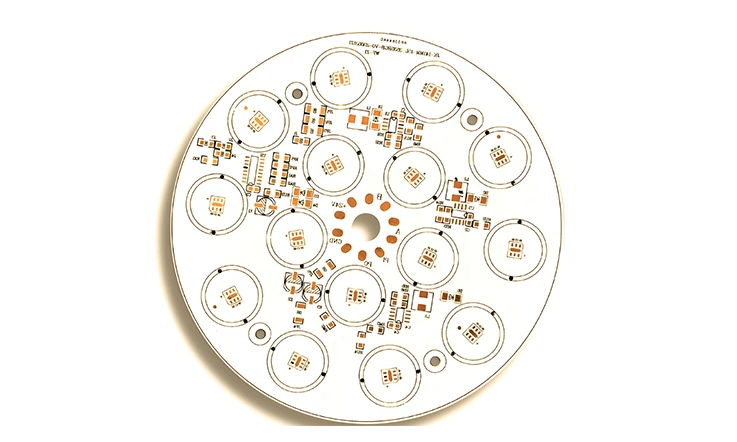
Bergquist HPL-03015 is a substrate material for printed circuit boards, architected upon an aluminum base. Its engineering purpose is explicit: to serve high-power electronics that demand both exceptional thermal conductivity and steadfast mechanical support. By virtue of its specialized material architecture, it offers an efficient thermal conduit, affording designers the ability to manage heat at the substrate level and thus lessening the reliance on bulky, costly external cooling apparatus.
Table 1: Key Material Properties of HPL-03015 IMS
| Property | Typical Value | Test Method |
| Thermal Conductivity (Dielectric) | 3.0 W/m·K | ASTM D5470 |
| Dielectric Thickness | 150 µm (0.15 mm) | Manufacturer Specification |
| Electrical Breakdown Voltage | > 3000 V | ASTM D149 |
| Volume Resistivity | > 10¹² Ω·cm | ASTM D257 |
| Flammability Rating | UL 94 V-0 | UL Standards |
The Tri-Layer Symbiosis: Copper, Dielectric, and Aluminum
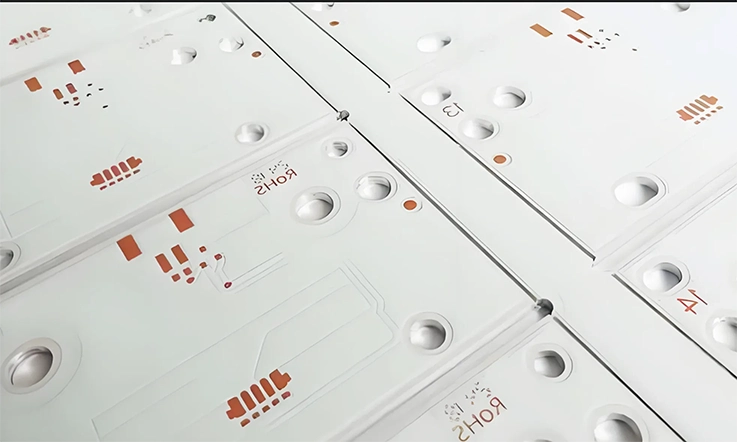
The typical form of HPL-03015 is a three-layer composite, a single, integrated unit delivered ready for circuit patterning and mechanical shaping. These three layers function like a symbiotic organism, each with its own function, yet inextricably linked.
●The Copper Circuit Layer: This uppermost stratum is the path for electricity, where the circuit blueprint is given life through chemical etching. Its thickness is specified to accommodate the anticipated current loads and trace densities.
●The Thermally Conductive Dielectric: This is the soul of the IMS material. The HPL-03015 dielectric is a proprietary blend of polymers and ceramic fillers, its molecular structure engineered for the efficient transfer of phonons (the carriers of heat energy) while its insulating nature impedes the free passage of electrons. It forges a bond between the copper and aluminum layers that is both thermally conductive and electrically insulating.
●The Aluminum Base Layer: This foundation, typically between 1.0 mm and 2.0 mm thick, serves the dual identity of a heat reservoir and a heat spreader. It rapidly absorbs thermal energy from the components above and uses its excellent conductivity to distribute that energy across its entire area. It also provides the finished board with a rigid skeleton, resisting flex and vibration.
Table 2: Tri-Layer Construction Details
| Layer | Material | Standard Thickness Range | Primary Function |
| Copper Circuit Layer | Electrolytic Copper | 1 oz – 3 oz (35 – 105 µm) | Signal and power conduction |
| Dielectric Layer | Ceramic-filled Polymer | 150 µm | Thermal transfer with electrical isolation |
| Base Layer | Aluminum (Alloy 5052) | 1.0 mm – 2.0 mm | Heat spreading and mechanical support |
A Natural Evolution Beyond FR-4 in Thermal Design
FR-4, an epoxy-glass laminate, is a practical and economical choice for many general-purpose designs. When heat becomes the design’s Achilles’ heel, its insulating nature becomes an insurmountable barrier. HPL-03015 introduces a paradigm shift in thermal thinking.
●A Direct Conduit for Thermal Flow: In stark contrast to the insulating character of FR-4, HPL-03015 lays a low-impedance highway for heat to travel from the fiery heart of a component, through the thin dielectric, and into the expansive aluminum base.
●Elevated Power Density: Through efficient thermal management, HPL-03015 allows engineers to arrange more powerful circuits in more confined spaces. Components can be placed in closer proximity without the looming risk of thermal runaway.
●An Inherent Uplift in Reliability: Creating a cooler operating environment for components like MOSFETs, LEDs, and power ICs has a direct and profound effect—their functional lifespan is extended, and the probability of physical failure due to long-term thermal distress is significantly diminished.
●Enduring Structural Integrity: The aluminum base endows the PCB with superior flatness and dimensional stability, effectively suppressing the warping and delamination phenomena common in large FR-4 boards subjected to repeated thermal cycling.
Section Essence: HPL-03015 is an aluminum-based substrate with a three-layer structure (copper, dielectric, aluminum) designed for superior thermal management. It provides a direct path for heat dissipation, enabling higher power density and greater reliability compared to traditional FR-4 materials.
Designing for Successful Fabrication of HPL-03015 PCBs
Interacting with an aluminum-based IMS material demands a design philosophy distinct from that used for traditional FR-4. Adherence to specific Design for Manufacturability (DFM) guidelines is an act of respect for the subsequent fabrication process. It smoothes the flow of work, minimizes the cost of rework, and lays the foundation for a robust final product.
Layout Fundamentals: Copper Spacing, Via Strategy, and Pad Design
Every copper feature on an IMS board has a subtle thermal and electrical relationship with the aluminum base below, requiring every design stroke to be considered.
Copper-to-Edge Clearance:
A “no-man’s land” of ≥ 0.5 mm should be maintained between any electrically active copper feature and the routed edge of the board. This gap serves as a trench to prevent surface flashover (arcing) during high-voltage operation and as a buffer zone to protect the copper from mechanical damage during routing.
Thermal Pad and Relief Design:
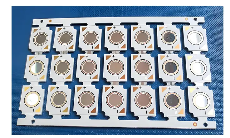
For heat-generating components like LEDs and power transistors, design expansive, solid copper pads to maximize the thermal contact area with the dielectric, providing a wide gateway for heat to enter. Conversely, for through-hole component leads not meant to dissipate heat, use “thermal reliefs.” These connect the lead to a large copper plane via a few thin copper spokes, preventing the surrounding copper from acting as a massive heat sink during soldering, which can make achieving a good solder joint difficult.
Via Strategy:
In high-density areas, stagger vias in a checkerboard pattern rather than aligning them in a straight line. This distributes mechanical stress and prevents the formation of a potential fracture line in the dielectric. For thermal vias, an array of multiple small-diameter vias is far more effective at dissipating heat than a single large one, as the total surface area of the via walls is greater, leading to more dispersed thermal flow.
Solder Mask Dam:
Apply a solder mask isolation strip (a “dam”) of ≥ 0.1 mm width around solder pads. During SMT assembly, this tiny dike effectively contains the molten solder, preventing it from flowing freely and causing a short circuit via a solder bridge.
High-Voltage Routing and Trace Width Considerations
For applications like electric vehicle converters and industrial power inverters, the safe guidance of high-voltage currents is a core design subject.
Creepage Distance:
For voltages of 250V or greater, a minimum surface creepage distance of 2.5 mm is recommended, especially near the board’s edge or around mounting holes. These areas are most prone to accumulating dust and moisture, and sufficient distance is the physical guarantee against contaminants forming a conductive path and causing an insulation failure.
Trace Width Calculation:
The IPC-2152 standard can serve as a starting point for calculating trace width for a given current load. Yet, wisdom lies in applying context. The superior heat dissipation of an HPL-03015 substrate means that for the same current, the temperature rise in a trace will be lower. This may permit the use of narrower traces than on FR-4, thereby saving valuable board real estate for the designer.
Rounded Corners:
At the corners of high-current traces, avoid sharp 90-degree angles and instead use smooth, rounded arcs. Sharp corners lead to a “current crowding” effect, much like water speeding up around a sharp bend in a river. This localized increase in electron density generates extra heat, creating a potential “hot corner.”
Routing Over Cutouts:
Avoid routing high-voltage or sensitive signal traces directly over milled cutouts or slots in the aluminum base. The vast difference in the coefficient of thermal expansion between the trace material (copper and dielectric) and the empty space (air) will cause continuous stress on the trace during every temperature change, potentially leading to a degradation of its adhesion or even a fracture over time.
Avoiding Common Pitfalls in IMS Design
Even seasoned designers can sometimes overlook the unique process variables of IMS boards. Avoiding these missteps at the source is the most efficient optimization of all subsequent process steps.
●Imprecise Dielectric Specification: A design file that vaguely specifies “IMS board” without explicitly stating the desired dielectric thickness (e.g., 75 µm vs. 150 µm) is like a recipe that calls for “a steak” without specifying the desired doneness. The final thermal and electrical performance of the product may diverge significantly from the designer’s expectation.
●Ignoring Mechanical Machining Stress: Placing plated through-holes or vias too close to a mechanically routed edge or cutout is a common oversight. The heat and mechanical vibration from milling the aluminum can be transmitted to the fragile plated barrel of the hole, potentially causing deformation or cracking.
●Heat Trapping by Copper Pours: A large, isolated copper fill that is not effectively connected to the aluminum base with thermal vias will not dissipate heat. Instead, it becomes a “thermal island.” It receives heat from components but has no efficient way to pass it on, leading to a local temperature that is higher, not lower.
●Unfriendly Board Outlines: While modern CNC equipment can create complex shapes, designs should still avoid extremely sharp internal corners or very narrow “necks” in the board outline. These features are difficult for a routing tool to navigate smoothly in an aluminum-backed panel, often resulting in burrs, tear-out, and the creation of mechanical weak points.
DFM Essence: Successful IMS design requires explicit specification of dielectric thickness, generous copper-to-edge clearances, strategic use of thermal reliefs and pads, and avoidance of sharp corners on high-current traces. Forethought regarding mechanical stresses from machining is also necessary for a robust outcome.
Advanced Thermal Management Strategies: Maximizing the Dissipation Potential of HPL-03015
Having a 3.0 W/m·K substrate is only the starting point. Optimal performance is realized through thoughtful layout techniques that effectively guide thermal flow, much like a precise and deliberate strategy in a complex system. Achieving this demands close technical collaboration between the layout engineer and the PCB manufacturers.
Mastering Thermal Via Arrays: Design, Density, and Placement
While standard IMS boards lack traditional plated-through holes that pass through the aluminum, the “thermal vias” created within the copper and dielectric layers are the fundamental means of opening low-impedance thermal “shafts” down to the aluminum base.
●Via-in-Pad Plated Shut (VIPPS): For maximum heat transfer from a component’s thermal pad, the recommended approach is a dense array of small-diameter (0.25 mm – 0.4 mm) vias directly under the pad. These micro-channels are then completely filled with a conductive or non-conductive epoxy and plated flat (planarized), creating a seamless, highly solderable surface that aggressively wicks heat away from its source.
●Optimal Via Density: The goal is to maximize the cross-sectional area of copper connecting to the base without compromising structural integrity. A tightly packed grid of small vias is more effective than a few large holes because it provides a more uniform and efficient thermal flow. Thermal simulation can help find the optimal balance between performance, complexity, and cost.
●Via Tenting: For thermal vias not located directly under a component pad, completely covering them with solder mask (a technique known as “tenting”) is an economical and effective method. It prevents molten solder from wicking into the via holes during assembly due to capillary action, which could otherwise “starve” the component’s solder joint.
Table 1: Thermal Via Design Guidelines
| Parameter | Recommended Value | Purpose |
| Via Diameter | 0.25 mm – 0.40 mm | Balance between heat flow and manufacturability |
| Via Pitch (center-to-center) | 0.7 mm – 1.0 mm | Ensures uniform via distribution |
| Fill Material | Non-conductive or conductive epoxy | Provides planar surface for soldering |
| Planarity (VIPPS) | ≤ 20 µm | Required for fine-pitch components |
| Tented Via Opening | Fully covered with solder mask | Prevents solder starvation during reflow |
Optimizing Heat Flow Through Strategic Component Placement
The spatial arrangement of components on the board, much like urban planning, has a profound impact on the overall thermal traffic flow.
●Centralize Major Heat Sources: When the design allows, place the highest power-dissipating components (e.g., power FET arrays, high-power LEDs) toward the center of the board. This allows the aluminum base to spread heat radially in all directions, like the ripples from a stone dropped in a pond, creating a more gentle temperature gradient.
●Distribute, Don’t Concentrate: If the design contains multiple significant heat sources, consciously distribute them across the board’s surface rather than clustering them together. This prevents the energy from multiple sources from overlapping and creating a single, massive “thermal storm center” that overwhelms the local dissipation capacity.
●Isolate Sensitive Components: Place components that are themselves not heat sources but are highly sensitive to temperature changes (e.g., precision voltage references, low-drift op-amps, quartz crystals) in the “cooler” regions of the board, far from major heat sources. When necessary, a “moat” free of copper can be designed around them to create a thermal break, acting as a firebreak between a hot “volcano” and a sensitive “village.”
Leveraging Copper Pours as Integrated Heat Spreaders
The copper layer on the board’s surface is itself an excellent lateral heat conductor. Using it wisely is a high-level design skill.
●Maximize Thermal Pad Area: The copper pad under a power component should be designed to extend beyond the component’s physical footprint. This extended “skirt” increases the initial surface area for heat to enter the dielectric, like widening the mouth of a river as it meets the sea, allowing for a smoother flow.
●Connect to Large Copper Fills: Connect the thermal pads of power components to large, uninterrupted copper planes or pours with wide copper traces. This utilizes the entire area of the copper plane for an initial lateral “pre-spreading” of the heat before it travels vertically down into the aluminum core, effectively blunting the peak temperature at the component.
●“Stitching” Pours with Thermal Vias: A very large copper plane that is merely “floating” on the dielectric will have its heat dissipation hampered. It should be periodically “stitched” down to the underlying aluminum base with a grid of thermal vias, much like quilting a blanket. These “stitches” ensure the entire plane remains in close thermal contact with the ultimate heat sink, preventing “smoldering zones” of trapped heat from forming within the pour itself.
Table 2: Copper Pour Heat Spreader Guidelines
| Design Strategy | Specification | Benefit |
| Thermal Pad Oversize Margin | +1.0 mm – 1.5 mm per side | Increases contact area with dielectric |
| Copper Trace Width to Pour | ≥ 1.5 mm | Ensures high current and heat flow capacity |
| Stitching Via Pitch | 1.0 mm – 1.5 mm grid | Maintains vertical thermal link to aluminum base |
| Copper Pour Thickness | 70 µm – 105 µm (2–3 oz) | Enhances lateral thermal transport |
| Inter-pour Thermal Isolation | Min. 1.0 mm if adjacent zones differ >20°C | Prevents heat migration to critical regions |
Thermal Management Essence: Beyond the material’s inherent properties, advanced thermal control is achieved through layout. This includes using dense thermal via arrays (especially VIPPS), strategically placing major heat sources centrally while distributing others, and using large copper pours stitched to the aluminum base to act as effective heat spreaders.
Mechanical Integration and Assembly: The Structural Considerations of HPL-03015 PCBs
An IMS board is not merely a platform for circuits; it is a structural component of the final product. Its mechanical properties and how it interacts with the rest of the assembly collectively determine its long-term reliability.
Mounting Techniques: Screw Fastening, Press-fit, and the Application of TIMs
Securely mounting the PCB is foundational for both mechanical stability and the effective transfer of heat to a chassis or larger heatsink.
The Art of Torque-Controlled Fastening:
When using screws for mounting, precise torque control is an art that must be mastered. Over-tightening can cause the rigid aluminum base to deform in ways invisible to the naked eye. This deformation can induce shear stress in the fragile dielectric layer and even cause the board to flex. Under-tightening, conversely, can leave microscopic air gaps between the PCB and the mounting surface. These gaps are thermal “canyons,” severely impeding the flow of heat. Calculating and applying the correct torque value is the only way to ensure a connection that is both secure and stress-free.
The Prudent Use of Thermal Interface Materials (TIMs):
Even two surfaces that appear perfectly flat are, at a microscopic level, a landscape of peaks and valleys. A thin, uniform layer of a high-quality TIM should always be applied between the aluminum base and the mounting surface. The purpose of this material is to fill those microscopic air voids, truly “welding” the two solid surfaces together and providing an uninterrupted bridge for heat to cross.
A Stable Foundation for Press-fit Connectors:
The rigid aluminum base of HPL-03015 provides an excellent, low-flex foundation for press-fit connectors. To ensure a reliable connection, the diameter of the holes and the plating thickness must be held to extremely tight tolerances, guaranteeing the connector pins create a tight, reliable, gas-tight electrical and mechanical bond when inserted.
Confronting the Challenge: Managing Coefficient of Thermal Expansion (CTE) Mismatch
In any assembly composed of multiple materials, managing how they expand and contract at different rates with temperature changes is a perpetual engineering challenge.
●The Physics of CTE Mismatch: Aluminum has a CTE of approximately 23 ppm/°C. Many electronic components, especially those with ceramic packages, have a much lower CTE (e.g., 6-8 ppm/°C). When the assembly goes through a temperature cycle, the aluminum base will “stretch” and “shrink” more than the ceramic component. This uncoordinated movement exerts a constant shear-like stress on the solder joints that connect the two.
Design Philosophies for Stress Mitigation:
●Prudent Component Selection: When functionality allows, give preference to components in smaller package sizes or those with flexible leads. Those flexible leads act like tiny springs, absorbing some of the strain from the CTE mismatch and thus protecting the fragile solder joint itself.
●The Art of Solder Joint Engineering: The solder joint is the front line in this stress battle. It is recommended to use more ductile (less brittle) solder alloys and to design larger, more robust solder fillets. A plump, pliable solder joint can endure long-term stress fatigue far better than a thin, rigid one.
●The Intervention of Underfill Adhesives: For large, high-risk components like BGAs, applying an underfill epoxy after soldering is an effective reinforcement technique. This epoxy flows under the component via capillary action and then cures, mechanically coupling the entire bottom surface of the component to the PCB, distributing stress and dramatically increasing its resistance to vibration and thermal cycling fatigue.
System Enclosure Co-Design: Extending the Thermal System
The design of the product’s housing should not be an isolated step; it should be co-developed in concert with the PCB design.
●The Chassis as Heatsink: The core design intent of an IMS board is to conduct heat efficiently to a larger mechanical structure. The product enclosure must be designed with a flat, smooth, and sufficiently large mounting surface that makes direct, solid contact with the PCB’s aluminum base. This surface is the final and most substantial stage of the entire cooling system.
●Creating Conditions for Convection and Radiation: The total heat generated by the system must ultimately be shed to the ambient environment. The enclosure design must facilitate this final step, either through thoughtfully designed ventilation slots that encourage natural air convection or by increasing the external surface area to enhance thermal radiation.
●Reserving Space for Electrical Safety: During the mechanical design of the structure, one must always be mindful of the live circuits on the PCB. An insurmountable air gap must be maintained between any live copper traces and any conductive surfaces of the enclosure to preclude any possibility of electric shock or short circuits.
●Mechanical Integration Essence: A successful assembly relies on precise screw torque, the correct application of TIMs to eliminate air gaps, and designing solder joints to withstand CTE mismatch stress. The system enclosure should be co-designed as the final stage of the heatsink, providing a direct thermal path and adequate ventilation.
Anatomy of an Expert Fabrication: The Precision Process for HPL-03015 PCBs
Transforming a sheet of HPL-03015 from raw material into a precision component is a journey of controlled transformation, a dance with the material’s properties. It embodies the craft of turning a design file into a reliable piece of engineering.
Stage One: Scrutiny and Preparation of Raw Material
The process starts with strict respect for the origin of the material. Each HPL-03015 panel must be verified against its lot traceability data to confirm its authenticity and known performance history. Following this, the panel is subjected to a specialized cleaning procedure designed to eliminate oils, particulates, and surface oxides. Achieving a clean and reactive surface is essential, as it lays the groundwork for effective bonding in all stages that follow.
Stage Two: Image Transfer and Circuit Etching
This is the stage where the board is given its electrical “soul.” Using high-precision photolithography, the customer’s design is transferred from a digital file to a photo-tool, and then projected onto the copper surface, which has been coated with a light-sensitive photoresist. After exposure and development, the panel proceeds into an automated spray etching line. Here, a carefully controlled chemical etchant dissolves the unprotected copper, leaving behind only the traces shielded by the hardened photoresist. For heavy copper, controlling the sideways etching (“undercut”) to achieve near-perfectly rectangular trace profiles is a challenge that showcases deep process knowledge.
Table 1: Photolithography and Etching Parameters
| Parameter | Typical Value | Process Control Method |
| Photoresist Thickness | 20–30 µm | Spin coating / dry film lamination |
| UV Exposure Energy | 200–300 mJ/cm² | Contact or stepper aligner |
| Etchant Type | CuCl₂ + HCl + Surfactant | Spray system with real-time monitoring |
| Etch Rate | ~1.5 µm/sec | Calibrated via coupon control |
| Trace Undercut (Target) | < 10% of copper thickness | Adjusted via chemistry and nozzle speed |
Stage Three: The Force and Finesse of Mechanical Processing
Drilling and routing on a hard aluminum base is like performing surgery on an armored patient, requiring a perfect blend of power and precision. The drills used are not standard bits; they are solid carbide tools with special geometries, paired with optimized spindle speeds and feed rates tailored for aluminum. This ensures the resulting hole is clean, smooth-walled, and free of burrs, without inducing delamination. When shaping the board’s outline, high-speed CNC spindles with diamond-tipped routing bits follow the programmed path, often using a multi-pass strategy to minimize mechanical stress and achieve a smooth, precise edge finish.
Stage Four: The Art of Thermal Curing for Solder Mask and Silkscreen
The solder mask is the colored “armor” that protects the circuits and prevents solder shorts during assembly. The liquid photoimageable solder mask ink is evenly applied, meticulously leaving all solder pads exposed. The panel then embarks on a journey through a long, tunnel-like oven with a carefully engineered “curing profile”—a gradual ramp-up, a soak at a specific temperature for full polymerization, and a slow cool-down to prevent thermal shock. This process determines the mask’s hardness, adhesion, and chemical resistance. Later, the silkscreen ink will undergo a similar, carefully controlled thermal curing process.
Stage Five: Surface Finish and Final Verification
The final steps are like framing and glazing a finished painting. To protect the exposed copper pads from oxidation and provide a solderable surface, a surface finish is applied. ENIG (Electroless Nickel Immersion Gold) offers an exceptionally flat surface, ideal for fine-pitch components. OSP (Organic Solderability Preservative) is an environmentally friendly choice that provides excellent solderability. After all processes are complete, every board is subjected to the unblinking eye of an Automated Optical Inspection (AOI) machine and a 100% high-voltage electrical test to confirm its graphical perfection and insulating integrity.
Table 2: Surface Finish and Final Inspection Parameters
| Operation | Standard Value | Verification Method |
| ENIG Coating Thickness | Ni: 3–6 µmAu: 0.05–0.1 µm | XRF (X-ray Fluorescence) |
| OSP Coating Thickness | 0.2–0.5 µm | Contact angle + wetting balance test |
| AOI Defect Detection Capability | Line width deviation ≥ ±20 µm | High-resolution CCD scanner |
| Electrical Test Voltage | 250–500 V (depending on net spacing) | Flying probe or fixture-based |
| Test Coverage | 100% net-to-net and net-to-copper void | IPC-9252 compliance |
●Fabrication Essence: Expert fabrication is a multi-stage craft, from material verification and cleaning to precision etching and mechanical processing with specialized tools. It culminates in controlled thermal curing for solder mask and a final surface finish, with 100% optical and electrical inspection as the final guarantee of quality.
Quality and Reliability: Inspection Standards and Advanced Verification
For applications where failure is not an option, product reliability does not stem from merely passing a test. It is born from an unwavering adherence to stringent industry standards and confirmed through the deep information provided by advanced inspection techniques. This is a commitment to a philosophy of quality.
Adherence to IPC-6012 Class 3/A for High-Reliability PCBs
The quality of a circuit board can be graded by internationally recognized IPC standards. It is possible to fabricate IMS boards to the highest level of reliability.
●IPC Class 2 (Standard): The common standard for most commercial and consumer electronics, ensuring reliable performance under normal operating conditions.
●IPC Class 3 (High-Reliability): Specified for applications where failure could have severe consequences, such as in automotive safety systems or aerospace electronics. It mandates tighter tolerances and has zero tolerance for certain types of defects.
●IPC-6012-Class 3/A Addendum: A specialized “super-standard” for the automotive industry, which builds upon Class 3 with even stricter requirements for thermal cycling endurance and ionic contamination control. Delivering a product to this standard is a testament to a profound dedication to quality control and process capability.
Beyond the Conventional: Advanced Non-Destructive Inspection Methods
To ascertain the integrity of the invisible structures within an HPL-03015 board, one must employ inspection methods that see beyond the surface.
●Scanning Acoustic Microscopy (SAM): This sophisticated non-destructive technique uses high-frequency ultrasound to inspect the bond line between the dielectric and the aluminum base. It can detect voids or delaminations that are invisible to the naked eye and can severely compromise thermal performance.
●X-Ray Fluorescence (XRF) Spectroscopy: XRF can be used after surface finishing to precisely measure the thickness and composition of the metallic layers, such as the nickel and gold in an ENIG finish, verifying both solderability and long-term corrosion resistance.
●Routine Micro-sectioning: Elevating micro-sectioning from a forensic tool to a routine, preventative “health check.” By systematically taking samples from the line and examining the cross-section under a microscope, one can continuously monitor the quality of drilling, plating, and other internal features, ensuring process stability.
The Final Guarantee: Documentation and a Traceability System
The value of a high-quality engineering artifact lies not only in its physical form but also in the complete, rigorous, and traceable documentation that stands behind it.
●Certificate of Conformance (CoC): A CoC delivered with a shipment is a formal declaration that the boards have been fabricated in strict accordance with the agreed-upon technical specifications and standards.
●Material Traceability: A complete traceability chain is maintained for all raw materials, including the specific roll and batch number of the Bergquist HPL-03015 used. This ability to trace a product back to its origins is indispensable for any root cause analysis.
●First Article Inspection (FAI) Report: For a new design, a detailed FAI report can be provided. This report documents all dimensional and electrical measurements of a first-off sample, offering objective evidence that the product meets all design criteria.
Quality Essence: Reliability is built on adherence to stringent standards like IPC Class 3/A. It is verified through advanced methods like acoustic microscopy and routine micro-sectioning, and guaranteed by a system of complete traceability and conformance documentation.
A Financial and Value Analysis: The ROI and TCO of HPL-03015
Selecting a premium substrate like Bergquist HPL-03015 is not a simple procurement act, but a strategic financial decision with a view toward the entire product lifecycle. The return on this investment is realized through reduced total system costs, lower field failure rates, and an extended, improved product life.
Lowering System Cooling Costs: Smaller Heatsinks and Fanless Designs
●Smaller or No Heatsinks: The thermal efficiency of HPL-03015 often allows designers to use significantly smaller external heatsinks, or in some cases, to eliminate them entirely. This directly saves material cost, reduces product weight, and simplifies assembly.
●The Possibility of Fanless Designs: By managing heat efficiently at the board level, human are more likely to achieve “fanless” silent designs. A system without a fan is not only quieter but also inherently more reliable, as a common mechanical failure point has been eliminated.
●A Smaller Product Footprint: Better thermal management enables higher component density, which leads directly to a smaller PCB area. This allows for smaller, lighter product enclosures, yielding savings in materials and shipping.
Reducing Field Failures and Maintenance Expenses
The root cause of many electronic failures can be traced back to heat.
●Fewer Thermally Induced Failures: By keeping components operating in a cooler environment, HPL-03015 dramatically slows the processes of solder joint fatigue, semiconductor degradation, and dielectric aging, leading to a lower rate of field failures.
●Lower Warranty Costs: A more reliable product translates directly into fewer warranty claims, lower repair costs, and a reduction in the brand reputation damage caused by product quality issues.
●Reduced Maintenance Needs: For equipment deployed in infrastructure, higher intrinsic reliability means a longer Mean Time Between Failures (MTBF), fewer service calls, and a lower total maintenance expenditure over the system’s lifespan.
Assessing Long-Term Value: An Improved Product Lifecycle
The initial purchase cost of an HPL-03015 PCB is merely the tip of the Total Cost of Ownership (TCO) iceberg.
●An Extended Product Life: According to the Arrhenius equation, a reduction in temperature can lead to an exponential increase in the lifespan of a semiconductor device. Keeping components cooler can substantially extend their functional life and that of the end product.
●Durable, Stable Performance: The material properties of HPL-03015 remain highly stable over tens of thousands of thermal cycles. This ensures the product’s performance at the end of its life is largely consistent with its performance on day one.
●A Higher Return on Investment: When measured by “cost per hour of operation,” the durability and reliability afforded by HPL-03015 provide a quantifiable and superior return on investment, especially in systems where downtime costs are extremely high.
Value Essence: The higher initial cost of HPL-03015 is offset by significant savings in Total Cost of Ownership. This is achieved by reducing or eliminating external cooling hardware, lowering field failure rates, and extending the product’s functional lifespan, resulting in a superior long-term return on investment.
Concluding a Masterclass: From Concept to Reality
The progression from technical specifications to a robust, high-performing assembly requires careful attention and well-informed engineering decisions. The concepts outlined here provide a solid framework for that process, guiding the transformation from base material to a dependable final result.
To take the final step, transforming your specific concept into a tangible reality, requires a deeper, collaborative dialogue. Engaging with thermal management specialists allows you to leverage dedicated expertise, ensuring your vision is not just fabricated, but masterfully realized.
Initiating a Technical Dialogue
A complete Request for Quotation (RFQ) package is the foundation for an accurate cost assessment and a constructive DFM feedback loop. This should include Gerber files (RS-274X), an NC drill file (Excellon), and a detailed fabrication drawing that specifies all requirements, including final thickness, copper weight, dielectric material and thickness, and desired surface finish.
Upon submission, every design receives a complimentary Design for Manufacturability review. This provides professional feedback on fabrication viability and offers a chance to discuss optimization, from stack-up selection to thermal via strategy, before any material is cut. This collaborative approach ensures your high-power project proceeds steadily from the first design concept to the final, perfect delivery.
FAQs about Bergquist HPL-03015 PCBs
1. For HPL-03015 boards, is V-cutting or Routing better for depaneling?
Routing is the preferred method. Due to the aluminum layer, V-cutting can create metal burrs and cause significant tool wear. Routing provides a smoother, more precise edge.
2. How significant is tool wear when processing HPL-03015?
Compared to FR-4, tool wear is significantly greater. The aluminum layer requires more durable tools (like carbide or diamond-coated bits) and optimized cutting parameters to extend tool lifespan and maintain precision.
3. How do you control trace width and undercut on heavy copper (3oz+) IMS boards?
We use differential etching, adjusting spray pressures and conveyor speeds. Our process includes advanced etchant regeneration to maintain chemical balance, ensuring tight trace width tolerances, typically ±10%.
4. For designs requiring aluminum pockets (milling), how do you control depth and protect the dielectric?
We use depth-controlled CNC routing with diamond-tipped end mills. The Z-axis depth is laser-calibrated to an accuracy of ±25µm, ensuring the pocket is created without compromising the dielectric layer’s integrity.


