
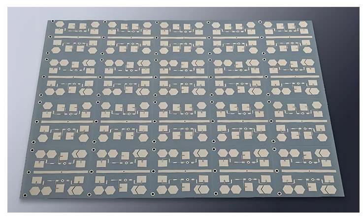
In high-frequency electronics, the selection of a PCB laminate is the foundational decision, the first sentence in a long and complex story of creation. A material like Taconic TLF-34 may present exceptional electrical properties on its datasheet, yet its true potential awakens only through the meticulous and experienced hands of a dedicated PCB fabricator. A flawless specification sheet is merely a promise; its value dissolves if the manufacturing journey fails to translate those ideal numbers into a reliable, high-performance printed circuit board.
This guide transcends the sterile landscape of datasheets. It offers a fabricator’s deep perspective on Taconic TLF-34, a narrative built on years of hands-on experience shaping this advanced organic-ceramic laminate. The following sections will dissect the intricate dance between material science, insightful Design for Manufacturability (DFM), and precision fabrication. The objective is to arm designers and engineers with the practical understanding needed to de-risk complex designs, accelerate development cycles, and achieve predictable, repeatable performance from a single prototype through to full-scale production.
Understanding Taconic TLF-34: Core Properties and Strategic Advantages
Taconic TLF-34 is a highly engineered composite material, thoughtfully designed to occupy the performance niche between conventional laminates like FR-4 and exotic pure-PTFE substrates. Its unique formulation—a blend of ceramic fillers within a woven-glass reinforced PTFE matrix—delivers a stable and predictable platform, a firm ground for engineers navigating the challenges of modern RF and microwave designs.
●Stable Dielectric Constant (Dk): A tightly controlled Dk of 3.40 ± 0.05 at 10 GHz ensures minimal variation between production batches. This stable dielectric property lays the foundation for producing controlled-impedance transmission lines and guarantees that simulated performance accurately reflects real-world hardware behavior.
●Extremely Low Dissipation Factor (Df): A Df of 0.0037 at 10 GHz signifies that a minimal amount of signal energy is lost to heat. This characteristic preserves precious signal power in high-gain amplifiers, filter networks, and long mmWave signal paths.
●Superior Thermal Stability (CTE): The X-Y axis CTE (17ppm/°C) closely matches that of copper. This synergy drastically reduces mechanical stress on vias and solder joints during thermal cycling, safeguarding the board’s long-term interconnect integrity in harsh environments.
●Enhanced Thermal Conductivity: Its ability to dissipate heat is roughly 50% better than FR-4. This provides a more efficient channel for cooling active components, leading to improved performance and a longer operational lifespan.
Why Expert Fabrication is Non-Negotiable for Taconic TLF-34?
Choosing Taconic TLF-34 reflects a strong focus on achieving top-tier signal integrity. However, its composite structure brings about manufacturing challenges far more complex than those encountered with standard FR-4. The difference between a successful, high-yield outcome and an expensive failure often depends entirely on precise process control and a deep, experience-based understanding of the material. The sensitive interplay between rigid ceramic fillers and flexible PTFE calls for refined techniques and a practiced approach to ensure reliable results.
A trusted manufacturers anticipates the material’s behavior through hands-on experience. They bring a deep, empirical understanding of how to fine-tune drilling parameters to avoid resin smear, how lamination cycles impact dielectric consistency, and how to apply precise etch compensation for exact impedance control. Working with a team well-versed in TLF-34 isn’t just about ordering a PCB—it’s a strategic move toward reducing risk, ensuring production reliability, and gaining the quiet assurance that the final hardware will deliver flawless performance in the field.
Precision Fabrication of Taconic TLF-34 PCBs: A Deep Dive
Mastery over the nuances of TLF-34 fabrication is what defines a specialized manufacturer. Achieving a reliable, high-performance product demands a suite of refined processes, each engineered to command the material’s unique ceramic-filled structure. This accomplishment is not merely about using the right equipment; it is born from a holistic system of process control, material-specific tooling, and the deep, practiced intuition of veteran technicians.
Advanced Drilling and Machining for Ceramic-Filled PTFE
While the ceramic filler in TLF-34 offers clear electrical advantages, it also renders the material highly abrasive and difficult to process. Conventional drilling techniques may lead to issues such as resin smear, fiber tearing, and delamination, all of which can undermine via integrity and signal performance. As a result, a carefully tailored approach is required to achieve high-quality hole formation—an core aspect of reliable manufacturing.
●Specialized Tooling & Parameters: Utilizing custom-geometry, hardened carbide drill bits. Spindle speeds, feed rates, and peck cycles are precisely controlled to prevent heat buildup and guarantee a clean, shear-like cut.
●Plasma-Activated Hole Walls: Employing a multi-stage CF4/O2 plasma process to chemically etch the hole wall. This action creates a micro-textured surface for superior copper plating adhesion, preemptively eliminating a common point of failure.
●Precision CNC Finishing: Using diamond-cut or multi-flute router bits for all routing and depaneling. This ensures smooth, defect-free board edges, minimizing stress points and preventing chipping during assembly.
Drilling & Machining Parameters Table:
| Parameter | Typical Value / Range | Notes |
| Drill Bit Type | Hardened Carbide, Custom Flute | Designed for ceramic-filled PTFE |
| Spindle Speed | 100,000 – 160,000 RPM | High speed to minimize mechanical stress |
| Peck Drill Cycle | 0.1–0.3 mm per step | Prevents material tearing and smear |
| Plasma Gas Mix | CF₄ + O₂ | Enhances hole wall adhesion |
| Router Type | Diamond Cut / Multi-Flute | Ensures clean routing with minimal burring |
Multilayer Lamination and Hybrid Stackup Expertise
Bonding multiple layers of TLF-34, or integrating it with other materials, requires absolute control over heat, pressure, and vacuum. The goal is to achieve a void-free, uniformly bonded structure without introducing stress or warping—a task made complex by the material’s unique properties and a true test of a fabricator’s skill.
●Tailored Lamination Profiles: State-of-the-art vacuum presses are employed with carefully designed, material-specific lamination profiles. Ramp rates and dwell times are precisely controlled to promote uniform resin flow, full encapsulation, and a stable final dielectric thickness across the entire panel.
●Hybrid Stackup Engineering: When combining TLF-34 with FR-4, symmetrical stackups are mandated to balance mechanical stresses and prevent warpage. Pre-baking cycles remove moisture from FR-4 layers, ensuring a robust bond between dissimilar materials.
●Uniformity and Thickness Control: The fabrication process maintains uniform final dielectric thickness across the panel, with tolerances commonly controlled within ±10%。This precise thickness control supports reliable impedance behavior in both buried stripline and offset stripline configurations.
Lamination Process Parameters Table:
| Parameter | Typical Value / Range | Notes |
| Vacuum Level | < 5 mbar | Ensures air-free lamination |
| Ramp Rate (Heating) | 1.5–2.5 °C/min | Controlled to avoid thermal stress |
| Press Temperature | 200–230 °C | Depends on bonding prepreg used |
| Press Pressure | 275–400 psi | Material-specific calibration |
| Dielectric Thickness Tolerance | ±10% | For both homogeneous and hybrid stackups |
Fine-Line Etching and Strict Impedance Control
The stable Dk of TLF-34 allows for finer trace geometries, but this places immense pressure on the etching process to maintain tight tolerances. Any deviation in trace width directly impacts impedance, potentially derailing the performance of the entire circuit. The process here is built around achieving and verifying this precision with unwavering focus.
●Predictive Etch Compensation: Applying sophisticated, empirically derived compensation factors to Gerber data. This proactively adjusts artwork to account for lateral etching, ensuring the final trace width on the board is precisely what the design intended.
●Universal Automated Optical Inspection (AOI): Scanning every single inner and outer layer with high-resolution AOI systems. This step verifies trace width and spacing down to the micron level and isolates any potential nicks, opens, or shorts before they are sealed within the board.
●Return Path Integrity Analysis: Performing a rigorous DFM check focused on maintaining uninterrupted ground planes. A continuous, low-inductance return path for high-frequency signals is a non-negotiable element for preventing EMI radiation and impedance discontinuities.
Etching and Impedance Control Table:
| Parameter | Typical Value / Range | Notes |
| Trace Width Tolerance | ±12 μm | Post-etch width measurement |
| AOI Resolution | ≤ 5 μm | Used for both inner and outer layers |
| Impedance Deviation | ≤ ±5% target | Verified through test coupon measurements |
| Etch Factor Adjustment | Empirically Derived | Applied at CAM stage |
Surface Finish Selection for Optimal RF Performance
The surface finish is the final, definitive interface between the PCB, the components, and the signals. The choice of finish directly influences solderability, signal loss at high frequencies, and long-term reliability. Guiding designers to the optimal choice is a reflection of a PCB fabricator’s holistic understanding of the product’s entire life cycle.
●ENIG (Electroless Nickel/Immersion Gold): Offers a perfectly planar surface well-suited for fine-pitch BGAs and QFNs. The nickel layer thickness is carefully controlled to prevent negative impacts on high-frequency signals due to the skin effect.
●Immersion Silver (ImAg): The preferred choice for mmWave applications (>20 GHz). Its excellent conductivity and low loss profile ensure maximum signal fidelity. The smooth TLF-34 surface provides an ideal substrate for a uniform, reliable silver deposition.
●OSP (Organic Solderability Preservative): A cost-effective and flat surface finish. It is well-suited for high-volume production, rapid prototyping, or non-sensitive sections of mixed-signal boards.
Advanced Interconnect Strategies for High-Density TLF-34 Designs
Modern RF and high-speed digital systems require integration levels that exceed the capabilities of conventional via technologies. Advanced interconnect methods are now required to shorten signal paths, minimize parasitic effects, and achieve higher performance targets. Applying these techniques effectively on a material such as TLF-34 reflects a high level of technical proficiency in manufacturing.
Blind, Buried, and Microvias for HDI
High-Density Interconnect (HDI) technology relies on non-standard vias to create connections only where needed, freeing up valuable routing space on other layers. The fabrication of these structures requires a sequential build-up process with multiple lamination and drilling cycles, demanding extreme precision and foresight.
●Sequential Lamination Process: Building the board in stages, fabricating and imaging internal cores first, then adding subsequent layers. This method allows for the creation of completely internal (buried) and partial-depth (blind) vias.
●Laser-Drilled Microvias: Utilizing precisely controlled laser systems to drill microvias (typically <150 µm). This enables extremely high-density fanouts from fine-pitch components, a gateway to miniaturization.
●X-Ray Guided Registration: Employing x-ray alignment systems before each lamination and drilling stage. This ensures layer-to-layer registration is held to incredibly tight tolerances, a testament to a dedication to precision.
HDI Via Fabrication Parameters Table:
| Parameter | Typical Value / Range | Notes |
| Laser Microvia Diameter | 75–150 µm | Dependent on component pitch |
| Microvia Aspect Ratio | ≤ 0.8:1 | Ensures plating reliability |
| Layer-to-Layer Registration | ±15 µm | X-ray alignment system |
| Blind Via Depth Control | ±10 µm | Via terminates accurately at target layer |
| Buried Via Layer Count | 4–12 | Common for high-density RF stackups |
Via-in-Pad Plated Over (VIPPO) for Miniaturization and Thermal Superiority
The VIPPO technique positions a via directly within a component’s surface-mount pad. This method enables efficient use of board space but demands a carefully controlled, multi-step process to prevent issues such as solder wicking during assembly. Accurate implementation of this technique reflects a high level of manufacturing expertise.
●Epoxy Via Filling: Completely filling the drilled via with a specialized conductive or non-conductive epoxy. This action eliminates any potential for solder to escape down the via barrel during reflow.
●Planarization and Capping: Grinding the filled via perfectly flat (planarization) and then plating it over with copper. This creates a solid, reliable surface that is indistinguishable from a standard SMT pad.
●Compounded Benefits: This approach enables direct component-to-inner-layer connection for ultimate space saving, the shortest possible signal path for improved signal integrity, and a highly efficient thermal conduit for cooling components.
VIPPO Process Control Table:
| Process Step | Standard / Range | Notes |
| Via Fill Material | Conductive or Non-Conductive Epoxy | Depends on thermal vs. electrical needs |
| Fill Uniformity | ≥ 95% of via volume | Ensures no voids or collapses during reflow |
| Surface Planarity | < ±10 µm | After grinding and before copper plating |
| Pad Diameter (Min.) | 400–500 µm | For typical 0.5–0.8 mm pitch components |
| Thermal Conductivity (if conductive) | ~3–5 W/m·K | Improves heat dissipation for power devices |
Controlled-Depth Drilling (Back-Drilling) for Pristine Signal Integrity
For multi-gigabit signals, the unused portion of a standard through-hole via acts as a resonant stub, reflecting signal energy and creating massive distortion. Back-drilling is a precision process that surgically removes this stub, preserving the signal’s purity.
●The Physics of Via Stubs: An unused via barrel segment behaves as an antenna, causing severe signal reflections and frequency-dependent losses that can cripple high-speed data channels. Understanding this is the first step to resolving it.
●Precision Secondary Drilling: After primary fabrication, using a Z-axis controlled drilling machine to re-drill the via from the stub side to a precise, calculated depth, removing the unused copper barrel.
●Enabling Extreme Data Rates: This process allows for clean signal transmission in systems operating at 10, 25, 56, and even 112+ Gb/s, where even minor imperfections have catastrophic consequences.
Back-Drilling Process Parameters Table:
| Parameter | Typical Value / Range | Notes |
| Stub Length After Drilling | ≤ 10 mil (254 µm) | Ideally 0 for high-speed designs |
| Drill Depth Tolerance | ±50 µm | CNC-controlled, based on signal layer depth |
| Min. Back-Drill Diameter | 0.2–0.3 mm above via ID | To ensure full barrel removal |
| Signal Performance Range | 10–112+ Gb/s | Supported with properly executed back-drilling |
| Material Compatibility | TLF-34 / Mixed Dielectrics | Validated on ceramic-filled PTFE-based boards |
A Masterclass in Signal Integrity for TLF-34 Boards
Signal integrity involves maintaining a signal’s original shape and timing as it travels to its destination. The PCB is frequently the main factor contributing to signal degradation. Maintaining waveform quality requires precise control of the physical transmission path and a thorough, experience-based understanding of the mechanisms behind loss, distortion, and noise.
Deconstructing and Minimizing Insertion Loss
Insertion loss represents the total signal power dissipated as it travels down a trace. At GHz frequencies, it is a primary concern composed of several factors, each of which must be actively managed with diligence during fabrication.
●Dielectric Loss: Energy absorbed and converted to heat by the TLF-34 material itself. Minimized by selecting this low-loss material and ensuring its properties are preserved through proper lamination.
●Conductor Loss (Skin Effect): Increased resistance as high-frequency current concentrates on the conductor’s “skin.” Mitigated by ensuring smooth copper plating and optimizing trace geometry.
●Copper Roughness Loss: At mmWave frequencies, the signal path follows the microscopic peaks and valleys of the copper foil, increasing path length and loss. This is managed by offering ultra-low-profile (VLP/ULP) and rolled-annealed (RA) copper foils, which are significantly smoother than standard options.
Manufacturing to Control Passive Intermodulation (PIM)
PIM (Passive Intermodulation) is a type of interference in high-power systems, occurring when two or more signals combine at a non-linear junction, producing unwanted additional frequencies. Such non-linearities may be unintentionally introduced during PCB manufacturing, and avoiding them reflects the rigor of the manufacturing process.
●PIM Sources on PCBs: It can result from variations in plating thickness, uneven trace edges caused by improper etching, or the use of specific metallic surface finishes (such as nickel) within the RF path.
●Process-Level Mitigation: PIM is controlled at its source through rigorous process control. This includes pristine plating bath chemistry, advanced etching for smooth trace sidewalls, and recommending low-PIM finishes like immersion silver for high-power applications.
Ensuring Phase Matching and Eliminating Skew in Differential Pairs
Differential pairs rely on two signals arriving at the exact same time. Any timing difference, or “skew,” compromises the system’s noise immunity. Skew can arise from physical length differences or variations in the dielectric material, and its management is a delicate task.
●Precision Length Control: The fabrication process maintains designed trace lengths to sub-mil accuracy. Any compensatory “serpentine” routes are reviewed to ensure they are designed with proper impedance control.
●TLF-34 Material Advantage: Unlike woven-glass materials, TLF-34’s uniform ceramic fill does not suffer from the “differential weave effect,” where one trace sees a different Dk than its partner. This provides an inherently more stable and homogeneous medium for high-speed differential pairs.
Engineering for Long-Term Reliability in Demanding Environments
A high-performance PCB must do more than function perfectly on a test bench; it must maintain its integrity over its entire operational life, often in unforgiving environments. The fabrication processes are specifically engineered to enhance the inherent robustness of Taconic TLF-34, ensuring it can withstand the thermal, mechanical, and environmental stresses encountered in demanding applications, from aerospace payloads to automotive radar.
Advanced Thermal Management Techniques
Effective thermal management is about more than just preventing component failure; it’s about maintaining stable electrical performance, as material properties like Dk can drift with temperature. The approach here is to create integrated thermal pathways within the PCB itself, a more elegant and efficient solution.
●Integrated Thermal Vias: Placing arrays of thermal vias directly under high-power components. These vias can be filled with thermally conductive epoxy to create an efficient, low-resistance channel from the component to internal ground planes or an external heatsink.
●Embedded Coins & Heavy Copper: For extreme power applications, solid copper or AlSiC coins can be embedded directly into the PCB stackup. Boards can also be manufactured with heavy copper layers (3 oz to 10 oz+) to spread heat laterally and manage high currents.
●Optimized Assembly Profiles: Providing clients with expert guidance on reflow soldering profiles. By recommending appropriate ramp rates and peak temperatures for TLF-34, maximum solder joint reliability can be achieved while preventing thermal shock during assembly.
Fortifying Mechanical Durability for High-Stress Applications
In applications exposed to shock, vibration, or frequent connector mating, the mechanical robustness of pads and vias is as important as their electrical performance. Certain manufacturing techniques can be used to strengthen these features, helping to avoid physical failure through careful and skilled process control.
●Reinforced Interconnects: Implementing teardrop-style pad-to-trace transitions and enlarged “anchor pads.” These features increase the copper surface area anchoring the pad to the laminate, dramatically increasing its peel strength and preventing pad lifting under stress.
●Structural Via-in-Pad: The VIPPO process transforms hollow via barrels into solid, reinforced posts by filling them with cured epoxy. This action significantly increases the via’s structural resilience to z-axis stress from thermal cycling and vibration.
●Edge Plating for Shielding & Grounding: Plating the milled edges of the PCB (castellation). This creates a continuous, robust conductive surface around the board’s perimeter for chassis grounding and 360-degree EMI shielding, enhancing both EMC performance and mechanical ruggedness.
Ensuring Resistance to Moisture, Vibration, and Thermal Cycling
A board’s ability to resist environmental factors is fundamental to its long-term reliability. TLF-34’s material properties provide an excellent starting point, which are then preserved and enhanced through meticulous process control and adherence to the highest industry standards.
●Low Moisture Absorption: TLF-34’s inherently low moisture absorption (<0.02%) prevents changes in Dk and mitigates the risk of Conductive Anodic Filament (CAF) failure in humid environments. The fabrication process ensures this property is maintained.
●Conformal Coating Adhesion: Utilizing surface preparation techniques that promote excellent adhesion for subsequent conformal coating operations, providing a robust barrier against moisture and contaminants.
●IPC-6018 Class 3/A Compliance: Manufacturing and certifying boards to the rigorous IPC-6018 Class 3/A standards for military, aerospace, and other high-stakes applications, which involves tighter tolerances and extensive reliability testing.
DFM for Taconic TLF-34: A Collaborative Path to Success
The best outcomes in high-frequency projects arise from an early and open collaboration between the design engineer and the manufacturing team. The Design for Manufacturability (DFM) process is approached as a constructive exchange, aligning ambitious performance objectives with the practical constraints of production. This collaboration provides the most effective way to balance yield, cost, and reliability, reducing the need for expensive redesigns.
Strategic Stackup and Layer Configuration
The stackup is the architectural foundation of the PCB. A well-planned stackup, developed in collaboration with the fabricator, is a defining element for achieving both electrical performance and mechanical stability.
●Symmetrical Construction: Advocating for symmetrical and balanced stackups for all multilayer boards. This practice balances mechanical stresses during lamination, virtually eliminating board warpage and ensuring via integrity.
●Expert Hybrid Integration: Possessing deep expertise in building hybrid stackups (e.g., TLF-34 cores with FR-4 outer layers) to balance performance and cost, ensuring CTE compatibility and a reliable bond between dissimilar materials.
●Stripline vs. Microstrip Guidance: Helping designers weigh the trade-offs. Stripline (internal) offers superior shielding and a stable Dk environment, while Microstrip (external) is simpler to route. Guidance is offered to find the optimal choice for sensitive nets.
Layout and Routing Guidelines for Signal Integrity
At GHz frequencies, the physical geometry of the layout directly governs signal integrity. The DFM feedback focuses on refining these geometries to eliminate sources of reflection and loss before fabrication begins, a task of preventative engineering.
●Fine-Line Capabilities: Offering a high-yield baseline of 5/5 mil (0.127mm) trace/space, with proven capabilities down to 3/3 mil for dense designs, supported by DFM consultation to ensure manufacturability.
●Smooth RF Transitions: Recommending and implementing tapered transitions and optimized co-planar waveguide (CPW) pad designs for connectors. This prevents abrupt impedance changes and minimizes signal reflections at launch points.
●Differential Pair Integrity: Verifying that differential pairs are tightly coupled and length-matched to minimize skew and noise conversion. Phase-matching serpentines are also reviewed to ensure they do not introduce their own impedance discontinuities.
Mitigating EMI and Crosstalk in Mixed-Signal Designs
When fast digital logic and sensitive analog or RF circuits are combined on a single TLF-34 board, controlling interference becomes a central focus of the DFM process. Careful advice on isolation techniques reflects a thorough and considered manufacturing approach.
●Physical and Electrical Partitioning: Advising on physical separation of circuit domains, reinforced with ground-stitched “via fences” or routed “moats” in copper planes to create effective isolation zones.
●Uninterrupted Return Path Design: Performing a deep DFM check to ensure high-speed return currents do not flow under sensitive circuits, and that low-inductance ground stitching is available near all signal layer transitions.
●Orthogonal and Shielded Routing: Recommending orthogonal routing in adjacent signal layers to minimize capacitive coupling. For maximum isolation, routing sensitive nets in a stripline configuration, sandwiched between solid ground planes, is the preferred method.
Mechanical Considerations: Panelization and Board Outline
DFM extends beyond the electrical design to include the mechanical aspects that ensure a board can be manufactured uniformly and assembled efficiently. These considerations are foundational for yield and cost.
●Copper Balancing for Plating Uniformity: Strategically placing non-functional copper patterns (“thieving”) in low-density areas of a design helps maintain even current distribution during electroplating. This supports uniform trace thickness and reduces the risk of localized distortion during lamination.
●Optimized Panelization for Assembly: Planning the optimal panel layout to maximize material usage and designing breakaway tabs or V-scores that are robust for assembly but allow for clean, low-stress depaneling, preventing damage to the board edge.
Taconic TLF-34 in Context: A Strategic Material Comparison
Choosing an appropriate laminate involves weighing factors such as electrical behavior, thermal performance, mechanical reliability, and cost. Insights from the manufacturing side can provide practical guidance informed by direct production experience. The following is a comparison of TLF-34 with other commonly used materials.
vs. Standard or High-Tg FR-4:
●Choose FR-4: For cost-driven projects with operating frequencies generally below 2-3 GHz. It is the workhorse for digital logic, power supplies, and low-frequency circuits.
●Choose TLF-34: When a design demands significantly lower signal loss, tighter impedance control, and stable performance across wide temperature ranges. The performance leap is substantial and necessary for high-fidelity applications.
| Property | Standard FR-4 | High-Tg FR-4 | Taconic TLF-34 |
| Dielectric Constant (Dk) | 4.2 – 4.8 | 4.0 – 4.3 | 3.4 – 3.6 |
| Dissipation Factor (Df) | 0.02 – 0.03 | 0.015 – 0.02 | 0.002 – 0.003 |
| Tg (Glass Transition Temp.) | ~130°C | ~170°C | ~280°C |
| Signal Frequency Range | < 2–3 GHz | Up to 5 GHz | Up to 20+ GHz |
| Thermal Conductivity (W/m·K) | ~0.3 | ~0.3 | ~0.9 |
vs. Rogers RO4003C:
●Similarities & Differences: Both are ceramic-filled laminates with comparable Dk values. RO4003C is widely recognized in the industry. Based on manufacturing experience, TLF-34 tends to offer improved dimensional control and smoother processing behavior, making it well-suited for complex builds involving multiple lamination cycles.
| Property | Rogers RO4003C | Taconic TLF-34 |
| Dielectric Constant (Dk) | ~3.38 | 3.4 – 3.6 |
| Dissipation Factor (Df) | 0.0027 | 0.002 – 0.003 |
| Tg (Glass Transition Temp.) | 280°C | ~280°C |
| Thermal Conductivity (W/m·K) | ~0.65 | ~0.9 |
| Dimensional Stability | ±0.1% | ±0.05% |
Sourcing and Handling Taconic TLF-34: A Supply Chain and Logistics Perspective
A successful high-frequency project involves more than design and manufacturing; it also requires a stable and reliable supply chain. Materials such as Taconic TLF-34 are not standard commodities, and their sourcing and handling demand specific expertise and procedures to preserve material quality and meet schedule requirements. Managing these logistical details with clarity and careful planning supports the overall success of the project.
Navigating the Supply Chain for High-Performance Laminates
The availability and stable performance of advanced laminates are important considerations for project managers and procurement personnel. Compared to standard FR-4, materials such as TLF-34 follow a more specialized supply chain, requiring careful planning and strong coordination with suppliers to manage lead times and maintain uniform material properties across different production batches.
●Authorized Sourcing Channels: Procuring all Taconic materials exclusively through authorized distributors. This action guarantees authenticity, full factory support, and an unbroken chain of custody from the manufacturer to the facility.
●Proactive Lead Time Management: Leveraging long-term forecasting and strong supplier relationships to anticipate and manage material lead times, ensuring a project schedule is not jeopardized by unforeseen shortages.
●Complete Lot Traceability: Maintaining meticulous records for every sheet of laminate, linking the final fabricated boards directly back to the specific manufacturing lot from Taconic. This provides a foundation for quality control and root cause analysis.
In-House Material Handling and Preparation Protocols
The moment TLF-34 laminate enters the facility, it is subject to strict handling protocols. The material’s PTFE-based composition makes it sensitive to environmental conditions and physical stress. Improper handling before fabrication can introduce latent defects that compromise final board performance, a risk that must be actively managed.
●Strict Climate-Controlled Storage: Storing all RF laminates and prepregs in a dedicated, climate-controlled environment with monitored temperature and humidity. This prevents moisture absorption, which can alter Dk and cause delamination during lamination.
●Thermal Stress-Relief Baking: Performing a controlled pre-baking cycle on the raw laminate before processing. This relieves any internal mechanical stresses accumulated during shipping and storage, ensuring dimensional stability throughout the fabrication process.
●Optimized Panel Preparation: Dedicated cutting and handling equipment is used to reduce physical stress on the material. When appropriate, panels are oriented according to the grain structure of the laminate to promote stable and predictable mechanical performance.
Assembly Considerations for Taconic TLF-34 PCBs: Beyond Bare-Board Fabrication
The fabrication of a high-quality bare board is only half the journey. The ultimate performance of the final product is decided during the Surface Mount Technology (SMT) assembly process. Assembling components onto a TLF-34 board presents unique challenges and opportunities compared to standard FR-4, requiring a deep understanding of solder interactions, thermal profiles, and component stress. Providing clients with guidance in this area is a way to ensure a successful transition from board to fully functional assembly.
Solder Paste Selection and Stencil Design
The first step in SMT assembly, the application of solder paste, is foundational. For fine-pitch components and RF circuits, the precision of this step is absolute. The choice of solder alloy and the design of the solder paste stencil must be carefully considered to ensure perfect solder joint formation without creating defects.
●Appropriate Solder Alloy: Recommending specific solder alloys (e.g., SAC305) that have excellent wetting characteristics with common surface finishes like ENIG and Immersion Silver, while also considering the thermal hierarchy required for complex assemblies.
●Precision Stencil Aperture Design: Designing stencil apertures with appropriate area reductions and home-plate shapes for fine-pitch components. This prevents solder bridging and minimizes the formation of solder balls, common issues in high-density assembly.
●Step Stencils for Mixed Components: Utilizing step-down or step-up stencils when a board contains both very small components requiring a thin paste deposit and larger components requiring a thicker deposit. This ensures the correct solder volume for every component on the board.
Component Placement and Reflow Profiling
The physical placement of components and the subsequent reflow soldering process must be carefully controlled. The high glass transition temperature (Tg) of TLF-34 allows for a wide processing window, but optimizing the reflow profile is the path to maximizing solder joint reliability and minimizing stress on both the board and the components.
●Calibrated Placement Force: Automated pick-and-place machines are used with carefully calibrated placement force. This approach helps prevent physical damage during assembly, particularly when handling delicate RF components and large BGA packages.
●Multi-Zone Reflow Oven Profiling: Developing a custom reflow profile for each assembly, with specific soak zones to activate flux and a carefully controlled peak temperature and time-above-liquidus (TAL). This ensures all solder joints are fully formed without overheating sensitive components.
●Inert Reflow Atmosphere: Recommending and utilizing a nitrogen (N2) atmosphere during reflow soldering. This inert environment reduces oxidation on both the pads and component leads, promoting better wetting and resulting in shinier, more reliable solder joints.
●Gradual and Controlled Cooling: Engineering the cool-down ramp of the reflow profile to be gradual. This action minimizes thermal shock and prevents the buildup of mechanical stress in the solder joints and the board itself, contributing to long-term reliability.
Real-World Success: Taconic TLF-34 Case Studies
Proficiency is reflected in practical outcomes. The following examples illustrate how these manufacturing approaches have been applied to produce TLF-34 PCBs used in demanding applications across highly regulated industries, where performance requirements allow no margin for error.
5G Infrastructure: Power Amplifiers and Phased-Array Antennas
In 5G systems, particularly Massive MIMO and mmWave deployments, efficiency and miniaturization are intertwined goals. The challenge is to create highly integrated antenna feed networks and power amplifiers that minimize loss and maintain precise phase control.
●Application: GaN Power Amplifier Matching Networks, Massive MIMO Antenna Feeds.
●Solution: Tightly controlled etching creates precise impedance-matching networks, while TLF-34’s low loss improves Power Added Efficiency (PAE). Its dielectric stability ensures identical phase relationships across large antenna arrays for accurate beamforming.
Aerospace & Defense: Radar Systems and SATCOM Transceivers
Reliability is non-negotiable in the arenas of aerospace and defense. These applications demand boards that can survive extreme g-forces, wide temperature swings, and intense vibration without any degradation in performance.
●Application: 77/79 GHz Automotive/Airborne Radar, Military SATCOM.
●Solution: Complex features like substrate-integrated waveguides (SIW) are machined directly into the TLF-34. Symmetrical stackups manage CTE stress, while robust grounding and shielding strategies are used to suppress PIM and crosstalk for secure communications.
Automotive and Industrial IoT: High-Frequency Sensors and Modules
The proliferation of connected devices requires compact, dependable, and high-performance RF circuitry that can be produced cost-effectively and operate reliably in often harsh environments.
●Application: Compact RF Modules, High-Reliability Industrial Sensors.
●Solution: TLF-34’s properties allow for finer traces and more compact components, enabling smaller module footprints. Its resistance to moisture and chemicals, combined with robust fabrication, ensures long operational life for sensors in industrial settings.
An Uncompromising Commitment to Quality: AS9100 & ISO 9001 Certified
In high-frequency applications, quality is integrated throughout the entire manufacturing process rather than being confined to final inspection. An AS9100 and ISO 9001 certified quality management system establishes a structured approach for maintaining process control and ensuring full traceability, supporting reliable outcomes and measured assurance.
Rigorous Raw Material Inspection and Traceability
The quality control process begins before the first cut is ever made. A flawless final product can only be built from flawless raw materials, a simple and powerful truth that guides every action.
●Certified Material Verification: Quarantining and inspecting every incoming batch of TLF-34, verifying certificates of conformance, checking for defects, and confirming all physical parameters.
●Independent Dk Validation: Fabricating and testing standardized coupons from new material batches to independently verify the dielectric constant meets the required specification.
●Climate-Controlled Storage: Storing all RF materials in a strictly monitored, climate-controlled environment to prevent moisture absorption and preserve their ideal electrical properties before use.
In-Process Quality Control (IPQC) at Every Stage
Multiple automated and manual inspection points are deployed throughout the fabrication flow to catch any deviation from the standard at the earliest possible moment, reflecting a belief in prevention over correction.
●Universal Layer Inspection: Using both AOI (for pattern defects) and AVI (comparison to Gerber data) on every single inner and outer layer.
●X-Ray Guided Alignment: Employing x-ray systems post-lamination to precisely measure layer-to-layer registration, a step that is fundamental for multilayer and HDI boards.
●Plating Thickness Measurement: Continuously monitoring plating bath chemistry and using non-destructive XRF equipment to verify the thickness of copper and surface finishes to meet IPC specifications.
Final Validation: Comprehensive Testing and Inspection
Before any board is shipped, it undergoes a final battery of tests to provide objective proof that it meets all electrical and mechanical requirements. This goes far beyond a simple electrical test, into the heart of the board’s character.
●Controlled Impedance TDR Testing: Measuring impedance on test coupons from every panel using a Time Domain Reflectometer (TDR), providing a report that validates the board’s high-speed performance.
●Micro-Sectioning Analysis: Routinely performing destructive cross-section analysis on coupons to visually inspect hole wall quality, plating thickness, layer registration, and the absence of defects under high magnification.
●100% Electrical Netlist Test: Performing a final bare-board electrical test on every single board using flying-probe or bed-of-nails testers, guaranteeing it is free of opens and shorts.
Advanced Testing and Electrical Verification Protocols for RF PCBs
For high-frequency PCBs, standard quality checks are insufficient. The invisible characteristics—how a board behaves at gigahertz frequencies—are what truly define its performance. A suite of advanced electrical verification protocols is deployed specifically to characterize RF performance and provide clients with empirical data, not just assumptions, about their finished product.
Active High-Frequency Performance Verification
Verifying connectivity through netlist testing and calculating impedance using stackup models alone does not provide a complete assessment. The approach centers on directly measuring the high-frequency performance of the finished board to obtain an accurate representation of its actual behavior.
●Vector Network Analyzer (VNA) Testing: For certain designs, a VNA can be used to measure the S-parameters (like insertion loss S21 and return loss S11) of specific traces or circuits on a test coupon or the board itself. This provides a true frequency-dependent characterization of the board’s performance.
●Passive Intermodulation (PIM) Testing: For high-power RF applications like antenna systems, the capability exists to perform PIM testing. This process injects two high-power tones into a device and measures the unwanted intermodulation products, a demanding test for ensuring clean communication channels.
Advanced Physical and Reliability Validation
Beyond standard micro-sections, advanced inspection and testing methods can be used to uncover potential latent defects and to validate the board’s robustness against environmental stresses, ensuring it meets the demands of high-stakes applications.
●Automated X-Ray Inspection (AXI): Utilizing AXI not just for layer registration but for detailed inspection of BGA pads and via-in-pad structures after fabrication, ensuring void-free and properly formed interconnects.
●Accelerated Thermal Shock Testing: Subjecting representative coupons to extreme temperature cycles (e.g., -55°C to +125°C) far beyond typical operating conditions. Subsequent micro-sectioning verifies that there is no cracking, delamination, or via failure.
●Conductive Anodic Filament (CAF) Resistance Testing: Performing biased humidity and temperature testing (e.g., 85°C/85% RH) to evaluate the material’s and the fabrication process’s resistance to the growth of conductive filaments between biased conductors, a deep measure of reliability for high-density designs.
A Manufacturing Partner: From Rapid Prototypes to Production
The overall process is structured to support complex projects with both flexibility and precision. It is designed to meet the requirements of fast turnaround times for prototyping while maintaining the strict process control required for accurate, low-to-medium volume manufacturing.
Accelerated Prototyping with Validated Process Models
Speed is a powerful advantage in the early stages of development. The prototyping service is designed to deliver high-quality, representative boards quickly, enabling faster design validation.
●Data-Driven Simulations: The CAM models are not generic; they are built on years of real production data from TLF-34, ensuring stackup and impedance predictions are a near-perfect match for the final physical board.
●In-House Material Stock: An inventory of common TLF-34 thicknesses and bonding materials is maintained, eliminating sourcing delays and compressing lead times for the first prototypes.
High-Mix, Low-Volume (HMLV) Production Excellence
The production floor is not designed for churning out millions of identical boards. It is specifically configured for agility and precision, making it highly efficient at producing smaller lots of many different, complex designs.
●Flexible Manufacturing: The processes and equipment are optimized for frequent changeovers, allowing for the production of small-to-medium lots (from one to several thousand pieces) without compromising quality or process control.
●Panel and Tooling Optimization: Advanced panelization software is used to maximize material utilization and minimize setup costs, making HMLV production highly cost-effective for clients.
Achieve Manufacturing Certainty with a Dedicated Taconic TLF-34 Partner
Taconic TLF-34 offers excellent performance for high-frequency applications, but it requires specialized handling and is not treated as a standard material. Achieving its full benefits—such as low loss, stable impedance, and high reliability—depends on a manufacturer with in-depth knowledge of the material, a disciplined approach to precision and quality, and a comprehensive understanding that spans from material sourcing to final assembly requirements.
The difference between a functioning design and a successful product depends on precise execution. Through collaborative Design for Manufacturability practices, accurate production processes, advanced interconnect techniques, and a structured quality and verification system, the path from design intent to a high-performance final product is clearly defined. This approach supports the goal of minimizing manufacturing variation, reducing development timelines, and providing a dependable foundation for demanding RF and microwave projects.
Questions (FAQ) about Taconic TLF-34 PCBs
Q: What is the typical maximum aspect ratio for vias on TLF-34 boards?
A: We can reliably achieve via aspect ratios of up to 10:1 on TLF-34. For designs requiring higher ratios, please consult with our engineering team for a DFM review.
Q: How resistant is TLF-34 to common solvents and cleaning agents?
A: The PTFE-based composition of TLF-34 gives it excellent resistance to most chemicals and solvents used during PCB assembly and cleaning processes.
Q: What are the standard manufacturing panel sizes for TLF-34?
A: We typically process TLF-34 on standard panel sizes such as 12″ x 18″ or 18″ x 24″. We can advise on the best panel utilization for your specific board dimensions to maximize cost-efficiency.
Q: What is the natural color of the TLF-34 laminate?
A: The TLF-34 laminate itself is typically an off-white or light tan color. On unmasked boards, this color can aid in the visual inspection of internal features.
Q: What specific bonding materials do you use for multilayer TLF-34 boards?
A: We commonly use Taconic’s own Tac-Bond™ or other qualified low-loss bonding films. The choice depends on the specific stackup requirements and operating frequency.


