Printed circuit boards (PCBs) have been integral components of electronic systems for close to 100 years, demonstrating their sustained importance. With the ongoing miniaturization of electronics, demand rises annually for compact, high-density PCBs. Cutting-edge manufacturing technologies now enable smaller circuit boards than ever previously possible. While PCB fabrication requires various materials and processes, it fundamentally relies on Gerber files.
So what exactly are Gerber files, and how are they generated? In this guide, I’ll walk through everything PCB designers need to know about these critical files.
Gerber Files Definition
The Gerber file format serves as the de facto standard in the PCB manufacturing industry, analogous to generating a *.pdf file after designing graphics or text documents. Nearly all PCB designers, whether hobbyists or professionals, have used Gerber files at some point. The format itself is an ASCII file type.
The Gerber format evolved from printing and plotting applications where it was used to recreate images and graphics. Similarly, in PCB design, Gerber files convey all the critical data from the source PCB file – tracks, holes, clearances, etc. – as printable graphics. Leading PCB CAD software can export PCB projects as Gerber files. These programs typically employ the RS-274-X variant of the Gerber standard, as it handles data efficiently.
For PCB designers, producing industry-standard Gerber files is a crucial step before sending a board out for fabrication. The files package all the layered graphical information fabricators need to replicate the design as a physical PCB. Overall, the Gerber format bridges the gap between PCB design software and manufacturing capabilities. As PCB designers, being fluent in generating proper Gerber output ensures our boards can be manufactured smoothly and accurately.
A Gerber file uses a basic ASCII vector format and contains the following elements:
● Configuration settings.
● Macro and aperture definitions.
● Draw and flash command codes.
● XY coordinate data.
Each drill span and image layer of the PCB design is exported as a separate Gerber file from the source design. For a simple two-layer board, over eight files may be transmitted to the PCB manufacturer, potentially including:
● Copper layer image for the bottom of the board.
● Copper layer image for the top of the board.
● Solder mask and silkscreen images for the bottom and top.
● Drill files showing hole positions and functions.
Plated and non-plated holes are often separated into different files. A complete PCB fabrication data package provides the manufacturer with all necessary instructions, such as required machining processes and other specifications. The comprehensive information in the Gerber files enables the PCB fabricator to accurately replicate the designed board.
What Should Include In Gerber Files?
To generate comprehensive Gerber files for PCB manufacturing, the following layers and information should be included:
Signal layers: All active signal layers carrying electrical connectivity must be enabled to produce corresponding Gerber files.
Plane layers: Like signal layers, all power and ground plane layers should be enabled to output Gerber files. Planes provide low-impedance power distribution.
Keepout layer: The board outline and non-conductive keepout zones should be delineated on a layer to clearly define electrical boundaries.
Mechanical layers: Any mechanical layers used for board outlines, mounting holes, etc. need to be enabled for Gerber generation even if they contain no electrical data.
Overlays: Top and bottom silkscreen overlays with component designators and reference markings need outputting.
Board dimensions: Overall PCB dimensions should be noted on the keepout layer or overlays for manufacturing reference.
Layer stackup: The board’s material stackup must be documented on a mechanical layer to provide details like core thickness, prepreg type, etc.
Timestamping: Dating the Gerber files aids version control and assists with any troubleshooting.
Verification: Use Gerber viewing software to validate file accuracy before release.
Thoroughly checking that the Gerber package contains all necessary fabrication data ensures the PCBs made match the intended design. Once validated, the files can be confidently transmitted to the manufacturer.
How to Generate the Gerber Files?
Generating Gerber files is a key part of the process of manufacturing printed circuit boards (PCBs) because these files provide all the necessary information about your PCB design to your manufacturer. Gerber files are a universally accepted standard for this kind of data.
The process of generating Gerber files varies slightly depending on the software you’re using, but the general steps are:
1. Design your PCB: You’ll first need to design your PCB with a software tool. There are many options available, including Eagle, KiCad, Altium Designer, and others.
2. Check your design: Before you can generate the Gerber files, you need to ensure that your design is correct and meets all necessary specifications. Most PCB software will have design rule checks (DRC) that can help with this.
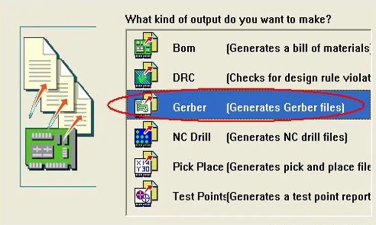
3. Generate Gerber files: Once your design is finalized and checked, you can generate the Gerber files. The exact method for doing this will depend on your software, but it generally involves selecting an option like “Fabrication Outputs” or “CAM Processor” and then choosing the Gerber format. Note that you’ll usually need to generate a separate Gerber file for each layer of your PCB, including the copper, solder mask, and silkscreen layers.
4. Generate NC Drill Files: Alongside the Gerber files, you should also generate NC Drill files. These files are used to guide the drilling process during PCB manufacturing.
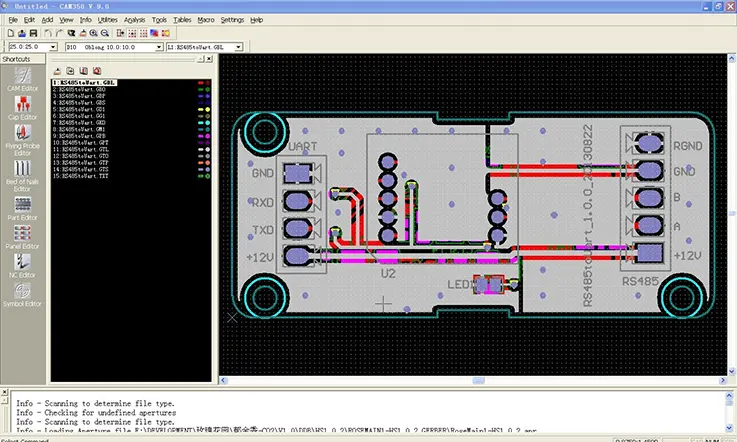
5. Inspect the Gerber files: After you’ve generated your Gerber files, it’s a good idea to check them using a Gerber viewer. This allows you to see exactly what your manufacturer will see and to check for any potential issues.
6. Send the Gerber files to your manufacturer: Once you’re satisfied with your Gerber files, you can send them to your manufacturer. They’ll use these files to manufacture your PCB.
Remember, generating Gerber files is a critical step in creating a successful PCB, so it’s important to take the time to get it right.
Kicad, Altium Designer and Eagle Software: How to Generate PCB Gerber Files?
As a PCB designer, we know it’s crucial to understand how Gerber file generation varies across design tools. Each program has its own workflow for producing the manufacturing data needed to get our boards fabricated. In this guide, we’ll share the specific steps I follow to create industry-standard Gerber files when I design PCBs with kicad, Altium Designer, and Eagle.
While the software packages differ, the end goal is the same – translating our schematics and layouts into the layered imaging information that PCB production facilities require. By carefully following the right file export procedures for each tool, we can ensure the Gerber files contain accurate fabrication data for every PCB layer. Before sending any board out for manufacturing, it’s essential that designers verify Gerber file integrity to avoid potential issues down the line. Knowing the ins and outs of generating proper Gerber output gives us confidence our boards will be produced as intended.
Kicad- Kicad Exporter Gerber
Here are the steps to generate Gerber files using Kicad:

1. Open the PCB project in Kicad. Go to File > Plot to open the plot dialog box.
2. Under “Plot Format” select “Gerber”
3. Enable the layers you want to output under “Layers to plot”. This typically includes:
● F.Cu (Top Copper Layer)
● B.Cu (Bottom Copper Layer)
● F.Mask (Top Solder Mask)
● B.Mask (Bottom Solder Mask)
● F.SilkS (Top Silkscreen)
● B.SilkS (Bottom Silkscreen)
● Edge.Cuts (Board Outline)
4. Under “Drill and Map Files” check the option to generate drill files.
5. Adjust other settings like output directory, file naming, units etc.
6. Click “Plot” to generate the Gerber and drill files.
7. The output folder will now contain the Gerber files, Excellon drill file, and drill map file.
8. Use a Gerber viewer to inspect the files before releasing to fabrication.
Following these steps in Kicad will produce the necessary Gerber manufacturing data from your PCB design, ready for sending to production.
Altium Designer- Altium Gerber Files
Here are the steps to generate Gerber files using Altium Designer:
1. Open the PCB project in Altium Designer.
2. From the menu, select File > Fabrication Outputs > Gerber Files. This will open the Gerber settings window.
3. In the layers tab, select all the layers you need to generate Gerber files for. Typically this includes:
● Top and Bottom Copper Layers.
● Solder Mask Layers.
● Silkscreen Layers.
● Drill Drawing Layer.
4. In the options tab, select the output directory and make any other adjustments to file naming, units etc.
5. Enable the “Generate Drill File” option to output the NC drill files.
6. Click on “Output All” to generate the Gerber and drill files. This may take some time depending on the board complexity.
7. The output folder will now contain the Gerber files, NC drill files and a Drill Map file detailing hole sizes and locations.
8. Use a Gerber viewer to inspect the files carefully before sending to fabrication.
Following these steps allows you to reliably produce industry-standard Gerber manufacturing data directly from your finished Altium PCB designs.
Eagle- Eagle Gerber Files
Here are the steps to generate Gerber files using Eagle CAD:
1. Open the PCB project in Eagle.
2. Run the CAM processor tool (File > CAM Processor).
3. In the CAM job, enable the following layers for Gerber output:
● op Copper
● Bottom Copper
● Solder Mask Top
● Solder Mask Bottom
● Silkscreen Top
● Silkscreen Bottom
● Board Outline
4. Check the “Use Route Commands” option.
5. Enable drill file output.
6. Set output directory and file naming preferences.
7. Click “Process Job” to generate the Gerber and drill files.
8. The output folder will contain the Gerber files (named per the layers), an Excellon drill file, and drill aid file detailing hole sizes and locations.
9. Use a Gerber viewer to verify the files before releasing to your PCB manufacturer.
Following these steps when using Eagle CAD will produce industry-standard Gerber files from your board design, containing all needed data for fabrication.
Gerber Files Play a Critical Role in PCB Manufacturing

Originally containing just basic configuration settings, macro definitions, and aperture sizes, Gerber files have evolved to encode more comprehensive fabrication data. While the core Gerber file format remains unchanged, the capabilities of PCB plotters and lasers have advanced significantly.
Modern PCB lasers still rely on the same Gerber file parameters to guide fabrication. However, the aperture limitations of earlier vector plotters no longer apply. Gerber data directs lasers on the precise locations and specifications for trace generation. Plotters translate the Gerber files into raster images to produce the PCBs.
Although Gerber file specifications continue to be enhanced, the format fundamentals persist for consistency. For the foreseeable future, this decades-old standard will likely experience only incremental changes, rather than a major overhaul. PCB manufacturers worldwide depend on Gerber files daily to translate design files into physical boards. Maintaining format continuity, while allowing measured improvements, helps sustain this vital manufacturing bridge.
Summary
The Gerber file format serves as the de facto standard for transferring information between PCB designers and manufacturers. Gerber files utilize the RS-274-X 2D ASCII format to convey all conductive, mechanical, text, and keepout layer data from the source PCB design, along with any necessary manufacturing notes.
Related Posts:
2. Gerber Files: Role in PCB Manufacturing
3. ODB++: The Ultimate FAQ Guide in 2023
4. Critical Information about Gerber Files for PCB Manufacturing
5. PCB Bill of Materials: A Comprehensive Guide to Effective Documentation