
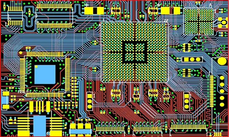
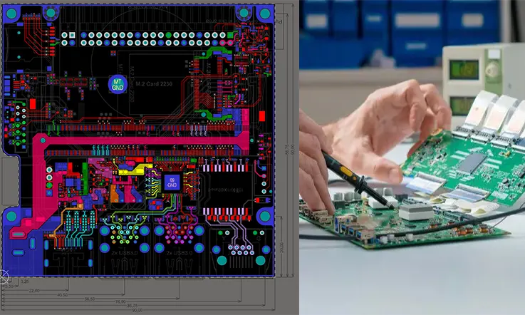
The production and design of PCBs are complex processes that involve mounting and connecting several components to a printed circuit board. Therefore, it is crucial to have a degree of control over this process. One of the most effective ways of ensuring that the PCB design and manufacturing process is error-free is through a design rule check (DRC).
Conducting a DRC early in the PCB design process can prevent further design flaws from occurring later on. By performing a PCB design rule check, one can ensure that the manufacturing process produces high-quality printed circuit boards with minimal errors. It is essential to identify and address any problems discovered during the DRC process promptly.
As professional PCB manufacturing and assembly factory, we understand the complexities and challenges involved in the PCB design and manufacturing process. That is why we employ the best practices and techniques for performing DRC checks to ensure that our products meet the highest standards of reliability, performance, and quality. Our commitment to excellence and attention to detail is evident in every aspect of our work, and we ensure that our customers receive the best possible PCB design and manufacturing services.
What Is a Design Rule Check ?
A design rule check, or DRC, is a set of guidelines that a PCB designer can follow to ensure that the schematic and board layout adhere to the specified dimensional tolerances and manufacturing requirements.
In any manufacturing process, deviations from a standard are inevitable. The ability of a fabrication firm to maintain consistency in its processes has a direct impact on the final quality of the product. Therefore, it is essential to design with allowances for the anticipated changes during production by including a sufficient margin in the design. This will ensure that the final design is functional and accurate.
By utilizing a DRC tool, a designer can verify that the schematic and layout accurately reflect the design margins that were included in the design. The DRC tool highlights any errors, such as a missing pin number, miswiring, shorts, or any other type of fault present on the schematic or layout.
At JarnisTech, we understand that a thorough design rule check is crucial to ensuring error-free production of high-quality PCBs. That is why we employ the latest tools and techniques to perform DRCs, and our professional team of PCB designers uses DRC to identify any mistakes and quickly resolve them. Our commitment to excellence and attention to detail ensures that our customers receive the best PCB designs along with reliable and efficient manufacturing services.
After completing the PCB design, it is crucial to check the design against the manufacturer’s specifications to ensure that it meets their published standard for acceptability. This step is known as the Design Rule Checking (DRC) process and serves as a quality control measure to ensure that the printed circuit board is built according to the intended specifications. The DRC will flag any design inconsistencies to the designer, who can make necessary adjustments to the layout and design to ensure compliance with the manufacturer’s specifications.
It is important to note that the design rules can vary widely between different PCB manufacturers. Hence, it is recommended that designers check the fabricator’s design guidelines thoroughly before submitting the design for production. By doing so, designers can ensure that their design adheres to the manufacturer’s specific requirements, increasing the chances of successful PCB fabrication. Finally, once the DRC process is complete, the designer can proceed with manufacturing the final PCB with confidence in the design’s accuracy and completeness.
Types of Design Rule Check (DRC)
There are several types of DRC checks that are commonly used in PCB design. These include:
● Electrical DRC: Checks for electrical violations such as open circuits, short circuits, impedance mismatches, and other signal integrity issues.
● Physical DRC: Verifies that the physical dimensions of the components and the board itself conform to the design constraints, including size, shape, and placement.
● Spacing DRC: Ensures that the spacing between components, vias, traces, pads, and other features meet minimum requirements to prevent electrical shorts and other issues.
● Manufacturing DRC: Checks for features that may cause problems during manufacturing, including drill holes that are too small, copper pads with insufficient clearance, and other issues that may affect the board’s yield and reliability.
● Design for Assembly (DFA) DRC: Evaluates the ease of assembling the finished PCB by checking for issues such as component placement and orientation.
● Design for Test (DFT) DRC: Verifies that the board can be easily tested for functionality and any embedded test structures, such as test points, are correctly placed.
Setting up DRC Rules and Parameters
Setting up DRC rules and parameters is a critical step to ensure that the DRC process is appropriately customized to the specific design requirements. To set up DRC rules and parameters, designers must follow these steps:
● Define the Design Rules: Define the rules for the selected DRC checks. These rules establish the design parameters, including traces, clearance, spacing, and other design attributes.
● Classify the Rules: Classify the rules as either Violations or Warnings. Violations are errors that must be fixed before the design can be released, while Warnings are design issues that do not necessarily require immediate correction, but may lead to problems if ignored.
● Create a Rule Check File: Create a rule check file that includes the rules and parameters to be checked during the DRC process. The rule check file can be created manually or with the help of a DRC software tool.
● Set the DRC Parameters: The DRC parameters may include defining the error criteria, specifying the allowable manufacturing tolerances, defining the manufacturing process parameters, etc.
● Run the DRC Check: Once the DRC rules and parameters have been defined and the rule check file has been created, the DRC check can be run. The DRC software will identify any rule violations or warnings and provide a report for the designer to review and correct.
Design Rule Check Software and Tools
There are several software programs and tools available to perform DRC checks in PCB design. Some of the popular ones include:
● Altium Designer: Offers a comprehensive set of design rules and DRC features, including the ability to customize rules and parameters.
● Cadence Allegro: Provides a powerful set of DRC capabilities, including real-time DRC and support for advanced design rules.
● Mentor Graphics PADS: Includes an extensive set of design rule libraries and customizable DRC rules.
● KiCAD: Offers powerful DRC capabilities for both commercial and open-source projects.
● Eagle PCB: Provides DRC tools and rule-checking features to help designers optimize the manufacturability of their PCB.
● HyperLynx DRC: A popular option for signal integrity and EMC analysis, including high-speed signal processing.
These software programs and tools help designers to set up design rules, run design rule checks, identify errors and warnings, and optimize the PCB design manufacturability. They can also help designers to customize their own DRC rules and parameters to ensure the best quality PCB design.
PCB Design Rule Checking and PCB Layout Combined
The integration of layout and DRC tools in PCB design brings convenience and efficiency, as designers can quickly run DRC tests from the PCB layout window. The DRC rules can be categorized into the following four distinct categories: safety, integrity, electromagnetic interference, and EMI. Furthermore, the DRC rule set includes a comprehensive overview page for each individual rule, allowing designers to prioritize which tests are most important to execute for their PCB layout.
High-speed nets crossing a split plane in a PCB design can create an impedance discontinuity on the signal trace, resulting in unwanted reflections, radiation, and crosstalk. However, locating and analyzing all instances of a net crossing a split plane can be a time-consuming and arduous task due to the complexity and density of modern PCB designs. In addition, standard simulation tools do not always check for these events.
The “nets crossing gaps” rule in DRC simplifies the process of identifying and locating potential discontinuities caused by high-speed nets crossing a split plane. By applying this rule in DRC, designers can pinpoint the specific locations of any instances of discontinuities that may occur. The implementation of this DRC rule can reduce the likelihood of errors and issues during PCB fabrication, ultimately leading to a more efficient and successful design process.
Best Practices for Design Rule Check Implementation
Here are some best practices for implementing DRC in PCB design:
● Define Clear Rules: Define clear and thorough design rules that are specific to the project requirements. These rules should include all electrical, mechanical, and manufacturing constraints.
● Create a Design Rule Checklist: Create a design rule checklist that helps to ensure that all DRC checks have been completed before the design is released for manufacturing.
● Perform Regular Checks: Perform regular DRC checks at each stage of the design process, including schematic and layout stages.
● Utilize DRC Software: Utilize DRC software tools that provide automated checks and real-time error feedback.
● Use Design Rule Templates: Use pre-defined design rule templates to create a consistent set of rules for your organization’s designs. This ensures that all designs conform to the company’s design standards.
● Collaborate with Manufacturing Teams: Collaborate with the manufacturing team to ensure that the DRC rules are appropriate for the manufacturing process.
● Keep Record of Errors: Keep records of errors and warnings found during DRC checks, as this data can be used to improve the design processes and optimize the design rules for future designs.
PCB DRC Rules
● Vertical Plane Change Rule: As a common design practice, routing traces from one layer to another is often necessary to achieve high packing densities in modern PCB layouts. However, it is crucial to take measures to limit the risk of common-mode radiation, which can lead to significant circuit performance issues. To address this, stitching capacitors or stitching vias are typically placed in close proximity to the net during a plane change. This facilitates a continuous current return path and minimizes the risk of common-mode radiation. The vertical reference plane change rule serves as a critical tool for identifying instances in which signals transition between layers and verifying the proper placement of stitching capacitors or vias in close proximity to those nets. This helps ensure that noise and interferences are minimized, and that the overall integrity of the circuit design is maintained. Ultimately, utilizing the vertical reference plane change rule is crucial for design engineers seeking to optimize circuit performance and minimize common-mode radiation risk.
● Crosstalk Coupling Rule: In circuit design, the crosstalk coupling rule is an essential tool for identifying regions where undesired crosstalk occurs on sensitive nets and highlighting these areas. Crosstalk can lead to significant timing and functional issues in the circuit and can be challenging to identify manually on a printed circuit board once manufactured. Furthermore, it can be difficult to isolate crosstalk from other aspects of the PCB design. As such, the crosstalk coupling rule is an invaluable resource for design engineers seeking to optimize circuit performance by swiftly pinpointing any problematic regions and taking appropriate action to rectify them. Ultimately, utilizing this rule can help minimize the negative effects of crosstalk and overall enhance the integrity of the circuit design.
● Filer Placement Rule: In circuit design, the filter placement rule is critical in ensuring that filters are located near the pins of a connector to minimize noise and protect sensitive communications from radiation. Without proper placement of filters, EMI issues may arise, resulting in potential system breakdowns. Therefore, adherence to the filter placement rule is essential in preventing severe EMI difficulties and maintaining the integrity of the overall system. Ultimately, verifying the presence and correct installation of filters on connectors is a fundamental step design engineers must undertake to ensure optimal circuit functionality.
● Decoupling Capacitor Placement Rule: In the daily work of an engineer, meeting the specified design parameters is a common challenge. Manually reviewing the location of decoupling capacitors on each net is a tedious and time-intensive process. One option for overcoming this challenge is to utilize DRC’s decoupling capacitor placement rule to identify any misplaced or missing decoupling capacitors related to a particular net or component. This rule offers an efficient and effective solution for achieving accurate decoupling capacitor placement, thereby improving the overall design quality while saving time and effort. Therefore, the decoupling capacitor placement rule is a valuable tool for design engineers seeking to optimize their design process.
● Signal Supply Rule: The signal supply rule is crucial in detecting any discontinuity between the reference plane of an integrated component’s connected traces and the planes that feed the component’s supply. Non-compliance with this rule can result in electromagnetic interference (EMI) issues and powerful radiation. Therefore, adherence to the signal supply rule is essential in ensuring the integrity of the integrated component’s reference plane and supply planes. Failure to comply may result in EMI breakdowns that could affect the overall performance of the circuit or even pose a potential safety hazard.
● Rule for DDR Signal Delay and Length Matching: In high-speed networks, timing plays a crucial role in the functionality of the network, particularly in DDR networks. Failure to adhere to appropriate timing limits for DDR signals arriving at their destination may result in memory malfunction. Timing issues may arise due to various factors, including transmission line propagation delay resulting from layer stack-up, dielectric characteristics, and trace routing. To address such issues, the delay and length matching rule can calculate necessary values automatically based on the design’s layer stack-up and perform checks for equivalent delays and/or lengths on each net in a specific group. This is necessary because delay problems are often a result of the unique physical characteristics of a PCB board. Therefore, the delay and length matching rule is essential in ensuring timing accuracy on high-speed networks like DDR.
● Power/Ground Width Rule: The power/ground width rule is essential in checking for insufficiently wide traces and ground traces in the design. Neglecting to follow this rule could result in insufficient current on that net, which can lead to a host of issues such as inadequate power delivery to components and excessive heat generation. It is important to note that while these issues are not exhaustive, they are some of the most significant problems that could arise from not adhering to the power/ground width rule, hence its importance in design engineering.
● Return Path Rule: To ensure that signals under examination have a low impedance return path, it is essential to adhere to the return path rule. In today’s high-speed circuit design, coupled with the shrinking size of PCBs, it is crucial to follow correct return path principles. Deviation from such principles can lead to electromagnetic interference (EMI) problems, where the return current on a trace fails to pass appropriately underneath the conductor and instead travels through other parts of the circuit, potentially causing EMI issues. It cannot be overstated that adhering to correct return path principles is of paramount importance.
● DDR Fly-by Topology Rule: In DDR systems that utilize a fly-by topology, the length of the stub plays a critical role in determining the performance of the architectural design. It is paramount to ensure that the nets established with a fly-by topology adhere to all pertinent design restrictions, and this is accomplished by applying the fly-by topology rule, which includes validation checks.
● Other Rules: Not to be found here. Get in touch with the JarnisTech PCB professional design team if you would like any further information regarding other DRC rules.
How DRC Can Help Cut Down on Board Re-Spins ?
Design Rule Check (DRC) is a valuable tool that can significantly reduce the number of board re-spins needed during a PCB design process. DRC is a software-based method of ensuring that a design meets the specific requirements and constraints necessary for successful manufacturing. By conducting automated checks against a set of rules, DRC can identify potential conflicts or issues in the design, enabling engineers to identify and correct issues early in the process.
As such, DRC helps to minimize the need for board re-spins by identifying problems in the design before it is finalized and manufactured. With DRC, potential issues such as component placement, routing errors, interference, and clearance issues can be detected and corrected early on, thus reducing the likelihood of costly and time-consuming rework later in the design process.
By using DRC, design engineers can also reduce the risk of undetected errors in the final product, ultimately resulting in higher quality circuit designs. Overall, the use of DRC has become an indispensable tool for design engineers seeking to reduce the need for board re-spins and achieve successful PCB manufacturing outcomes.
DRC and PCB Manufacturing
DRC is a critical step in the PCB design process that ensures that the design meets the requirements for successful manufacturing. The DRC rules and parameters are defined to ensure that the design conforms to the specific manufacturing process requirements.
Here are some ways DRC can impact PCB manufacturing:
● Ensuring Manufacturability: The DRC checks are performed to ensure that the design meets the criteria necessary for successful manufacturing, including material constraints, fabrication constraints, and assembly constraints.
● Improving Yield: DRC checks can identify and prevent design errors that could result in poor yield rates. By identifying and addressing these issues before manufacturing, yield rates can be improved.
● Reducing Cost: By addressing potential manufacturing issues during the design phase, designers can help to reduce the cost of the PCB fabrication process, reduce turnaround time, and minimize the risk of late-stage design changes.
● Enhancing Performance: DRC checks can identify and rectify signal integrity issues, such as impedance mismatches or crosstalk, resulting in improved performance of the PCB.
● Meeting Standards: DRC checks enable designers to verify that their design meets industry standards, regulatory requirements, and customer specifications.
As a result, performing DRC checks is crucial to ensure that the finished design effectively achieves its intended function, performs optimally, is reliable, and can be successfully manufactured.
Importance of Design Rule Check in PCB Design
PCB Design Rule Check (DRC) is a crucial step in the PCB design process that ensures the design’s manufacturability and reliability by detecting potential errors and violations of design rules before the board is fabricated. DRC verifies the design against a set of predefined design rules and constraints, including electrical, physical, spacing, and manufacturing rules.
The importance of DRC lies in its ability to identify and correct design flaws early in the design cycle, reducing the cost and time associated with prototype iterations and rework. By performing DRC, designers can ensure that their designs are optimized for manufacturability, functionality, and reliability.
Common DRC Errors and How to Fix Them ?
There are several common DRC errors that can occur during the PCB design process. Here are some examples, along with suggestions for how to fix them:
● Clearance Violations: Clearance violations occur when components, vias, or traces are too close to one another. To fix this error, you can adjust the placement of the affected components, vias, or traces.
● Short Circuits: Short circuits happen when two or more conductive features are unintentionally connected, causing a direct path for electrical current to flow. To fix this error, separate the affected conductive features by creating a gap between them.
● Unconnected Nets: This error occurs when a net on the schematic is not connected to any pins in the layout. To correct this error, connect the affected nets by adding vias or traces to connect the net from the schematic to the layout.
● Missing Footprints: This error occurs when the footprint for a component is not defined or does not match the specified component. To correct this error, add the missing footprint to the library or replace the missing component with a properly defined component.
● AssertionError: This error occurs when the given condition is not true. This error can have multiple causes, including corrupted files and unexpected data. The fix for this error will depend on the specific cause, but may involve reviewing the design files, updating the software, or seeking assistance from the software provider.
By identifying and correcting these common DRC errors, designers can ensure that their PCB design is error-free and optimized for manufacturability, functionality, and reliability.
Future Developments in DRC Technology
DRC technology has come a long way since its inception, and there are still several emerging trends that will shape its future development. Here are a few potential future developments in DRC technology:
● Integration of AI: Artificial intelligence (AI) may be integrated into DRC technology to drastically improve the accuracy and speed of DRC checks. By training AI models with vast amounts of design and manufacturing data, it can generate accurate design rules and detect design errors in real-time with high accuracy.
● Machine Learning Algorithms: Machine learning algorithms can analyze massive amounts of data and identify complex failure modes, learn from them, and avoid these failures in future designs.
● Simulation-based DRC: Simulation-based DRC enables designers to simulate DRC checks before running them, allowing them to test the design and make adjustments to the rules before running the actual checks.
● Compliance-checks & Certifications: DRC systems of the future could include compliance-check for safety and environmental regulations and certifications, allowing designers to verify their designs meet specific regulatory and industry standards for safety, environmental compliance, and quality.
● Cloud-based DRC Processing: The future of DRC could be cloud-based to improve the scalability of processing and reduce the need for expensive processing power on local machines.
DRC technology is continually advancing, and future developments will improve manufacturability, reliability, and performance of the PCB design process while also increasing efficiency. These innovations will support the continued growth of the PCB industry and reduce costs and time-to-market for new designs.
.
Summary
In the PCB design process, errors with DRC can be very common, which is why performing a PCB design rule check is a crucial step in manufacturing high-quality boards. As PCB and PCBA manufacturers, we have the responsibility to ensure that we comply with this guideline by employing the best practices and techniques to fabricate top-quality products.
If you would like to learn more about DRC for PCB manufacturing and how we apply these industry standards to our manufacturing processes, we invite you to contact us today. Our professional team of PCB design engineers is dedicated to ensuring that our products meet the highest standards of quality, reliability, and performance. We look forward to the opportunity to discuss your project needs and to demonstrate how our expertise and commitment to excellence can help you achieve your goals.


